

Page 1

DVP-F5/FX1
RMT-D114A
SERVICE MANUAL
Photo: DVP-FX1
Manufactured under license from Dolby Laboratories
Licensing Corporation.
“DOLBY” and the double-D symbol ; are
trademarks of Dolby Laboratories Licensing
Corporation.
US Model
Canadian Model
AEP Model
UK Model
Chinese Model
DVP-FX1/F5
Hong Kong Model
DVP-FX1
Australian Model
DVP-F5
SPECIFICATIONS
PORTABLE CD/DVD PLAYER
Page 2
— 2 —
Page 3

SAFETY-RELATED COMPONENT WARNING!!
COMPONENTS IDENTIFIED BY MARK 0 OR DOTTED LINE WITH
MARK 0 ON THE SCHEMATIC DIAGRAMS AND IN THE PARTS
LIST ARE CRITICAL TO SAFE OPERATION. REPLACE THESE
COMPONENTS WITH SONY PARTS WHOSE PART NUMBERS
APPEAR AS SHOWN IN THIS MANUAL OR IN SUPPLEMENTS
PUBLISHED BY SONY.
SAFETY CHECK-OUT
After correcting the original service problem, perform the following
safety checks before releasing the set to the customer.
ATTENTION AU COMPOSANT AYANT RAPPORT
À LA SÉCURITÉ!
LES COMPOSANTS IDENTIFÉS PAR UNE MARQUE 0 SUR LES
DIAGRAMMES SCHÉMATIQUES ET LA LISTE DES PIÈCES
SONT CRITIQUES POUR LA SÉCURITÉ DE FONCTIONNEMENT.
NE REMPLACER CES COMPOSANTS QUE PAR DES PIÈSES
SONY DONT LES NUMÉROS SONT DONNÉS DANS CE MANUEL
OU DANS LES SUPPÉMENTS PUBLIÉS PAR SONY.
1. Check the area of your repair for unsoldered or poorly-soldered
connections. Check the entire board surface for solder splashes
and bridges.
2. Check the interboard wiring to ensure that no wires are
"pinched" or contact high-wattage resistors.
3. Look for unauthorized replacement parts, particularly
transistors, that were installed during a previous repair. Point
them out to the customer and recommend their replacement.
4. Look for parts which, through functioning, show obvious signs
of deterioration. Point them out to the customer and
recommend their replacement.
5. Check the B+ voltage to see it is at the values specified.
6. Flexible Circuit Board Repairing
• Keep the temperature of the soldering iron around 270˚C
during repairing.
• Do not touch the soldering iron on the same conductor of the
circuit board (within 3 times).
• Be careful not to apply force on the conductor when soldering
or unsoldering.
— 3 —
Page 4

TABLE OF CONTENTS
1. GENERAL
About this manual ··························································· 1-1
This Player Can Play the Following Discs ······················1-1
Precautions ······································································ 1-2
Notes about the Discs ······················································1-2
Getting Started
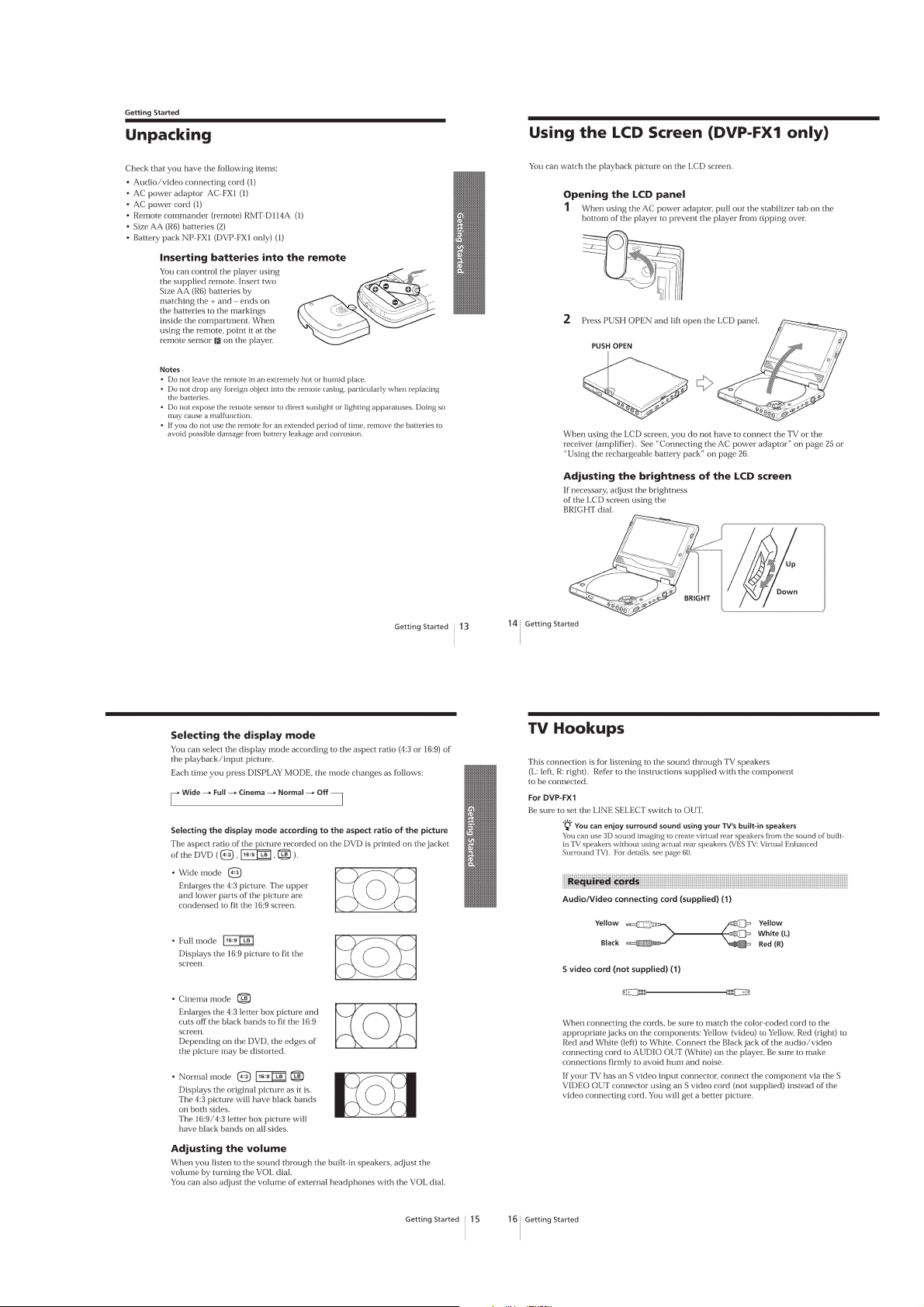
Unpacking ······································································· 1-3
Using the LCD Screen (DVP-FX1 only)·························1-3
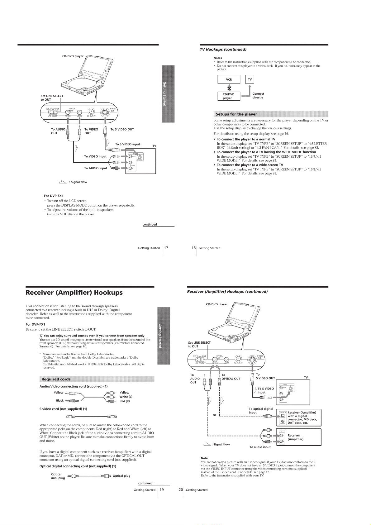
TV Hookups ···································································· 1-3
Receiver (Amplifier) Hookups ········································1-4
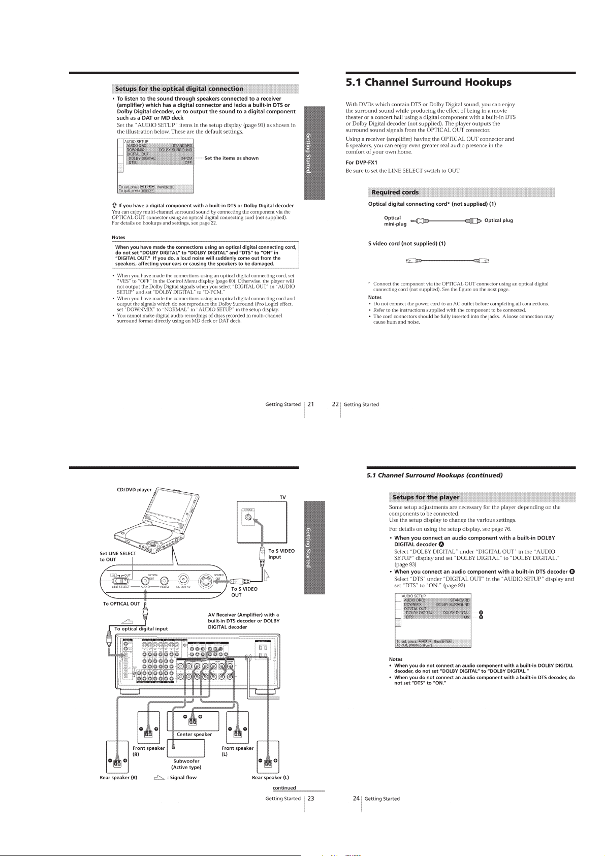
5.1 Channel Surround Hookups ······································ 1-5
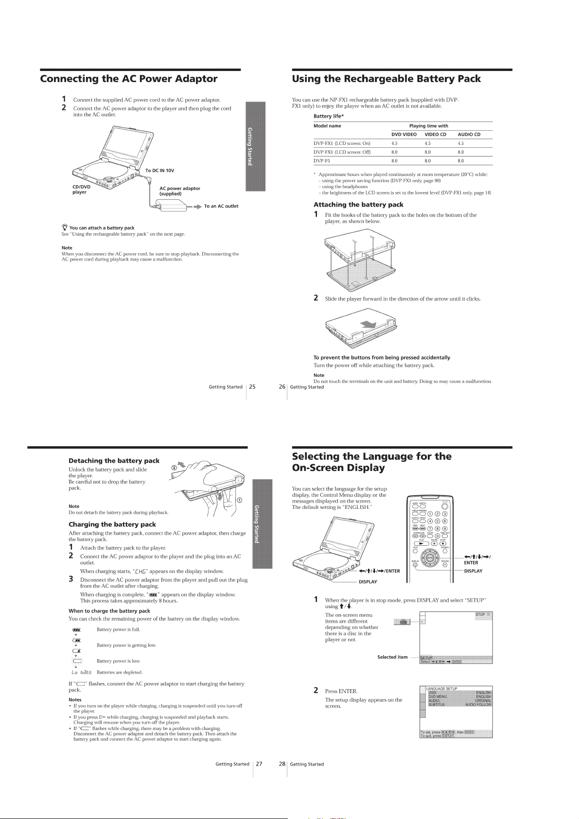
Connecting the AC Power Adapoter································ 1-6
Using the Rechargeable Battery Pack ····························· 1-6
Selecting the Language for the On-Screen Display ········ 1-6
Plaing discs
Playing discs ···································································· 1-7
Searching for a Particular Point on a Disc ······················ 1-8
Resuming Playback from the Point Where You
Stopped the Disc (Resume Play) ································1-8
Using the DVD’s Menu ··················································· 1-9
Playing VIDEO CDs with PBC Functions
(PBC Playback) ·························································· 1-9
Using the Display Window ············································1-10
Using Varioius Functions with the Control Menu
Using the Control Menu Display··································· 1-11
Control Menu Item List ·················································1-11
Searching for a Title/Chapter/Track/Index/Scene ········· 1-12
Cheking the Playing Time and Remaining Time ··········· 1-12
Selecting a Starting Point Using the Time Code ···········1-12
Viewing the Disc Information ······································· 1-13
Cheking the Sound ························································ 1-13
Displaying the Subtitles················································· 1-14
Changing the Angles ····················································· 1-14
Digital Cinema Sound Settings ····································· 1-14
Checking the Play Information ······································ 1-15
Locking Discs (Custom Parental Control) ···················· 1-16
Creating Your Own Program (Program Play) ················1-16
Plaing in Random Order (Shuffle Play) ························ 1-17
Plaing Repeatedly (Repeat Play) ···································1-18
Repeating a Specific Portion (A-B Repeat) ·················· 1-18
Settings and Adjustments
Using the Setup Display ················································1-18
Setup Display Item List ·················································1-19
Setting the Display Language or Sound Track
(LANGUAGE SETUP) ············································ 1-19
Settings for the Display (SCREEN SETUP) ·················1-20
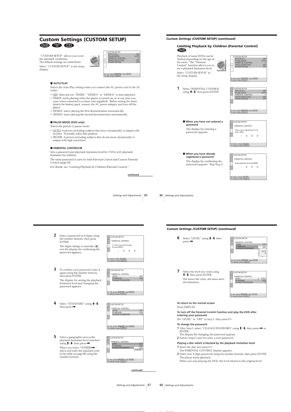
Custom Settings (CUSTOM SETUP) ··························· 1-21
Settings for the Sound (AUDIO SETUP)······················ 1-22
Preventing the Buttons from being Pressed
Accidentally······························································ 1-23
Additional Operations
Listening with Headphones ···········································1-23
Watching the Picture without Connecting Cables
–LASER LINK ························································· 1-23
Watching the Picture of Other Equipment on the
LCD Screen (DVP-FX1 only) ··································1-24
Additional Information
Troubleshooting····························································· 1-24
Self-diagnosis Function ·················································1-26
Language Code List······················································· 1-26
Index to Parts and Controls ··········································· 1-26
2. DISASSEMBLY
2-1. Cabinet Assy-1 ································································ 2-1
2-2. Cabinet Assy-2 ································································ 2-1
2-3. Cabinet Assy-3 ································································ 2-1
2-4. CD, LID ··········································································· 2-2
2-5. MB-90 Board, LC-68 Board, MD Comple ····················· 2-2
2-6. Display Panel (FX1) ························································2-3
3. BLOCK DIAGRAMS
3-1. OVERALL BLOCK DIAGRAM (1/2) ··························· 3-1
3-2. OVERALL BLOCK DIAGRAM (2/2) ··························· 3-3
3-3. VIDEO OUT BLOCK DIAGRAM ································· 3-5
3-4. RF BLOCK DIAGRAM (1/2) ········································· 3-7
3-5. RF BLOCK DIAGRAM (2/2) ········································· 3-9
3-6. AUDIO BLOCK DIAGRAM ········································3-11
3-7. LCD BLOCK DIAGRAM ············································ 3-13
3-8. POWER BLOCK DIAGRAM (1/2) ······························3-15
3-9. POWER BLOCK DIAGRAM (2/2) ······························3-17
4. PRINTED WIRING BOARDS AND
SCHEMATIC DIAGRAMS
4-1. FRAME SCHEMATIC DIAGRAMS ····························· 4-1
4-2. PRINTED WIRING BOARDS AND
SCHEMATIC DIAGRAMS ············································ 4-4
• LC-68 (LCD) PRINTED WIRING BOARD ··············· 4-5
• LC-68 (LCD) SCHEMATIC DIAGRAM ···················· 4-6
• MB-90 (RF, VIDEO, AUDIO, SERVO,
SYSTEM CONTROL)
PRINTED WIRING BOARD ························· 4-7
• MB-90 (1/12)(DC-DC CONVERTER)
SCHEMATIC DIAGRAM ····························4-11
• MB-90 (2/12)(D/D CONV, BATT, CHG)
SCHEMATIC DIAGRAM ····························4-13
• MB-90 (3/12)(SIGNAL PROCESSOR)
SCHEMATIC DIAGRAM ····························4-15
• MB-90 (4/12)(SERVO (1))
SCHEMATIC DIAGRAM ····························4-17
• MB-90 (5/12)(SERVO, DSP)
SCHEMATIC DIAGRAM ····························4-19
• MB-90 (6/12)(ARP, DRAM)
SCHEMATIC DIAGRAM ····························4-21
• MB-90 (7/12)(AV DECODER)
SCHEMATIC DIAGRAM ····························4-23
• MB-90 (8/12)(16M SDRAM)
SCHEMATIC DIAGRAM ····························4-25
• MB-90 (9/12)(SYSTEM CONTROL)
SCHEMATIC DIAGRAM ····························4-27
• MB-90 (10/12)(IF CONTROLLER)
SCHEMATIC DIAGRAM ····························4-29
• MB-90 (11/12)(AUDIO IN/OUT)
SCHEMATIC DIAGRAM ····························4-31
• MB-90 (12/12)(VIDEO IN/OUT SELECT)
SCHEMATIC DIAGRAM ····························4-33
• MB-90 WAVEFORMS ··············································4-35
• TP-61 (1/3)(DC-DC CONVERTER)
SCHEMATIC DIAGRAM ····························4-39
• TP-61 (2/3)(RGB DECODER)
SCHEMATIC DIAGRAM ····························4-41
• TP-61 (3/3)(TIMING GENERATOR)
SCHEMATIC DIAGRAM ····························4-43
• TP-61 (TIMING GEN, RGB DECODER)
PRINTED WIRING BOARD ······················· 4-45
• TP-61 WAVEFORMS ·············································· 4-47
5. IC PIN FUNCTION
5-1. SYSTEM CONTROL (MB-90 BOARD IC002:
MB91107PFV-G-BEN) ··················································· 5-1
5-2. IF CONTROL (MB-90 BOARD IC701:
M37513MB-055GP) ·······················································5-3
— 4 —
Page 5

6. TEST MODE
6-1. GENERAL DESCRIPTION ··········································· 6-1
6-2. STARTING TEST MODE ··············································· 6-1
6-3. SYSCON DIAGNOSIS ··················································· 6-1
6-4. DRIVE AUTO ADJUSTMENT ······································ 6-5
6-5. DRIVE MANUAL OPERATION ···································6-7
6-6. EVR ADJUSTMENT ······················································ 6-9
6-7. EMERGENCY HISTORY ············································ 6-11
6-8. VERSION INFORMATION ········································· 6-12
6-9. VIDEO LEVEL ADJUSTMENT ·································· 6-12
6-10. SELF-DIAGNOSIS OF IF CONTROLLER ················· 6-12
7. ELECTRICAL ADJUSTMENT
7-1. POWER SUPPLY BLOCK (TP-61 BOARD)·················7-1
7-2. SYSTEM CONTROL ADJUSTMENT
(TP-61 BOARD) ····························································· 7-2
7-3. VIDEO SYSTEM ADJUSTMENT ································· 7-2
7-4. ARRANGEMENT DIAGRAM FOR ADJUSTMENT
PA RTS ············································································· 7-4
8. REPAIR PARTS LIST
8-1. EXPLODED VIEWS ······················································ 8-1
8-2. ELECTRICAL PARTS LIST ·········································· 8-7
— 5 —
Page 6
SERVICE NOTES
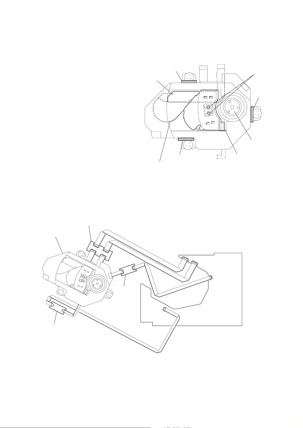
1. REPLACING OPTICAL PICK-UP
1-1. Handling
1) A red laser diode for DVD requires more attention to static
electricity than general infrared laser diodes for CD.
Because its durability to static electricity is far weaker than
that of infrared laser diodes, always use an earth band when
handling the optical pick-up block as service parts.
Double-sided
adhesive tape
Hold position
From
spindle motor
From optical
block pick-up
Objective lens
2) The optical pick-up of the DVP-F5/FX1 cannot be replaced as
a single part. It is supplied as the MD COMPLE (DVDMFX1).
Note: When the MD COMPLE is going to be replaced, be very
careful not to damage the flexible board to peel off the
flexible board because the flexible board is attached
underneath the cabinet by the double-sided adhesive tape.
3) When handling the MD COMPLE (DVDM-FX1), be careful
not to touch the portions specified in the illustration of the MD
COMPLE with hand. Be sure to hold the hatched portions
described as “HOLD” in the illustration.
1-2. Connection of the DM flexible extension
board (J-6090-101-A) for service
For any attempt is going to be made to inspect, check and adjust
the MB-90 board, connect the DM flexible extension board as
shown below.
OP-CN
MD COMPLE
( DVDM-FX1)
16-pin flexible board (114mm)
Hold position
Flexible board
From
sled motor
Hold
position
Turntable
(spindle motor)
Lens actuator
covers
SLED-CN
18-pin flexible
board
(114mm)
SPDL-CN
7-pin flexible board (194mm)
CN802 (16 pin)
CN801 (18 pin)
CN804 (10 pin)
10-pin flexible board
(114mm)
CN803
(7 pin)
MB-90 board
— 6 —
Page 7
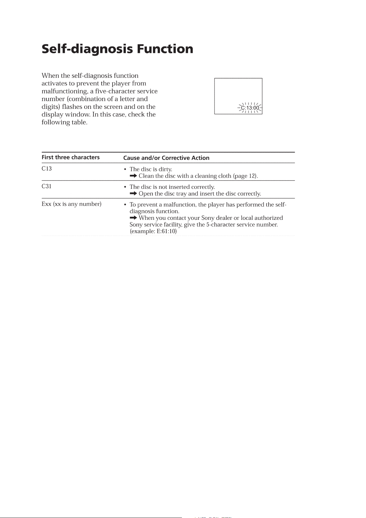
SELF DIAGNOSIS
— 7 —
Page 8

MEM
O
— 8 —
Page 9
SECTION 1
GENERAL
DVP-F5/FX1
This section is extracted from
instruction manual.
1-1
Page 10

1-2
Page 11
1-3
Page 12
1-4
Page 13
1-5
Page 14
1-6
Page 15

1-7
Page 16

1-8
Page 17
1-9
Page 18

1-10
Page 19
1-11
Page 20

1-12
Page 21
1-13
Page 22
1-14
Page 23
1-15
Page 24

1-16
Page 25
1-17
Page 26

1-18
Page 27
1-19
Page 28
1-20
Page 29
1-21
Page 30
1-22
Page 31

1-23
Page 32

1-24
Page 33

1-25
Page 34

1-26
Page 35

1-27
Page 36

1-28E
Page 37

SECTION 2
e
)
DISASSEMBLY
NOTE: Follow the disassembly procedure in the numerical order given.
2-1. CABINET ASSY-1
2 Screws (M1.7 × 4)
Cabinet Assy
3
DVP-F5/FX1
2 Screws (M1.7 × 4)
Robber foot rotary tabl
(FX1 only)
1
2-2. CABINET ASSY-2 (FX1)
Fulcrum cover (R)
Fulcrum cover (L
1 Screws (M1.7 × 4)
2-3. CABINET ASSY-3 (FX1)
1
2
2-1
Page 38

2-4. CD, LID
)
3 Compression spring
CD, LID
Plate(CD LID) Assy
3
ful crum
1 Screw (M1.7 x 3)
2 Tension spring
(open)
2 Open blacket
1 Screw (M1.7 x 3)
4 Lock lever
2-5. MB-90 BOARD, LC-68 BOARD, MD COMPLE
2
MD Comple (DVDM-FX1)
1
1
SRS selection knob
1
MB-90 Comple
I/O selection knob (FX1 only
LC-68 Comple
Cursor button
Hold knob
2-2
Page 39

2-6. DISPLAY PANEL (FX1)
LCD cover
2
Inverter
qa
PWB flexible
3 Screws
Speaker
Link chassis assy
9 Screws (M1.7 x 2)
TP-61 comple
6
0
7
5 Screw
4
8 Screws
Open button (LCD)
qs
Display panel
3 Screws
Speaker
3 Screws
1 Screws
(M1.7 x 4)
LCD cushions
4
3 Screws
1 Screw
(M1.7 x 4)
LCD cushion
LCD cabinet
2-3
1 Screws
(M1.7 x 4)
LCD cushion
Lock claws
LCD cushion
Page 40

MEM
O
2-4E
Page 41

BLOCK DIAGRAMS
3-1. OVERALL BLOCK DIAGRAM (1/2)
SECTION 3
DVP-F5/FX1
OPTICAL DEVICE
DVD
PDIC/LD
MODULE
CD
LD/PD
COUPLER
MODULE
DVD
TRK/FCS
COIL
CD
TRK/FCS
COIL
MD BLOCK
M901
SPINDLE
MOTOR
M
M
M902
SLED
MOTOR
LIMIT
A
B
C
D
LD
PD
RF
CD-E
CD-AL
CD-F
PD1
PD2
CP-PD
CD-LD
TRK–
TRK+
FCS–
FCS+
CDF+
CDF–
CDT–
CDT+
SPON
PHDA
SLD–
SLD+
EC
HFGI
LIMSW
MB-90 BOARD
SIGO
XLDON
IC801
RF
IC805
FOCUS
/TRACKING
COIL
DRIVE
IC813
IC808
SLED MOTOR
DRIVE
IC811
SPINDL
MOTOR DRIVE
MIRR
TZC
PI
FE
TE
DFT
SCLK
SDATA
SDEN
IN1
IN3
IN2
IN4
SRDR
SFDR
(SEE PAGE 4-13,15,17,19,21,23,25,27,29,33)
Q812
SW
DOOR SW1
DOOR SW2
GI03
TO S713
TO S714
IC952
IC802
BUFF
IC812
ERROR
AMP
SSCK
SSDATA
SSCS
SPON3
FCD–
FCD+
TRD–
TRD+
TGIN
PWM0
PWM1
PWM2
FGIN
PG REF
SDSP
CLKIN
2
8
HRD
HWR
RS
RFIN1,2
MDP0
MDS0
LOCK
HA0,1
HD8-15
IC602
ARP2
SDI0-7
CDDATA
CDDOUT
MA0-9
MD00-15
CDBCK
CDLRCK
SDEF
XSAK
XSRQ
XSHD
XDCK
XWAT
8 HD8-15
8 HA0-7
XRD
XWR
ARPRST
XCS
XINT
WE
OE
RAS
UCAS
LCAS
BCK
LRCK
SPDIF1
IC603
MEMORY
ARINT
XARPCS
ARPRST
LRCK0
CD1N1I
CD1N2I
IREQ0
ISTARTI
HWATTOB
HD0-15 16
WRHRDXRST
BCK0
IERRI
IVALI
ICLKI
RSTB
ACH12
27M
512FS1
IC005
ACH34
ACH56
VIDEOV
VIDEOY
VIDEOC
ADDT0-15
ADADT0-11
DOHL
DOMU
SDCS0B
SDCS1B
TRST
DM-ACK0,1
DM-REQ0,1
HIRREQ0
HAD22,23
SCLKIN
CLKIN
CRPCLKI
ACLK
22 HA0-21
TO
IC301
IC302
PLL
WE
CAS
RAS
CLK
CKE
3
6
512FS2
33M
27M
44.1/48K
CS
CS
X002
27MHz
IC351
VIDEO AMP
IC653
IC654
16M SDRAM
(IC653)
(IC654)
DACK0,1
DREQ0,1
XAVINT
XAVDCS2,3
IC003
RESET
D0
7
IC652
A/V DEC.
HA0-21
HD0-15
DVP-F5
IC353
C SW
CONTROL
S701-704
FUNCTION
S705-708
FUNCTION
VMUTE-TFT
V-IOCNT
VIDEOSW
XFRRST
KEY
KEY
V
Y
J351
VIDEO OUT
VIDEO IN/OUT
J352
S VIDEO OUT
DVP-FX1
IC352
VIDEO SW
KEY1
(DVP-F5)
(DVP-FX1)
S351
LINE SELECT
IN/OUT
C
KEY2
KEY3
IC701
IF-COM
IC354
C SW
S709
FUNCTION
KEY
IR
(1/2)
VIDEO OUT
IC702
REMOTE CONTROL
RECEIVER
C OUT
V-IOCNT
ACH12
ACH34
ACH56
BCK
LRCK
SPDIF1
XRST
ON PAGE
3-3
IC703
XRESET
HA0-21
HD0-15
HD0-15
HA1-20
ECS
EBSY
WC
R/B
RESET
IC001
CS
EEPROM
WE
OE
IC004
FLASH
MEMORY
16M
CE
XRDMCS
48/44.1K
XFRRST
DACK0,1
DREQ0,1
XAVINT
XAVDCS2,3
WIDE
EWC
SIN1
SOUT1
SCLK11
DO
DI
SK
SI0
SO0
SC0
XIFCS
TEMP
TH701
XIFBSY
HIN
HCS
SDSPINT
XSDSPCS
IC002
(1/2)
SYSTEM CONTROL
16
3-1
3-2
Page 42

DVP-F5/FX1
3-2. OVERALL BLOCK DIAGRAM (2/2)
ON PAGE
3-2
LC-68 BOARD
(SEE PAGE 4-6)
ND1001
VIDEO OUT
C OUT
V-IOCNT
ACH12
ACH34
ACH56
BCK
LRCK
SPDIF1
XRST
512FS
TO
IC005
D1006
D1012
MB-90 BOARD
(SEE PAGE 4-29,31)
COM0-3
SEG0-16
SDI0
SDI1
SDI2
BCKI
LRCKI
MCLK
MCLK
SO
SCK
XCS
IC301
AUDIO DSP
SI
SD00
TO
Q812
S713
S714
S711
S712
S715
S716
S710
FUNCTION SW
R
L
R
L
DOORSW2
DOORSW1
DVP-F5
IC305
LINE AMP
X701
4MHz
DOORSW1
DOORSW2
TFTOPEN
SRSSW
DVP-FX1
XOUT
LCDPCON
PLAY
POWER
HOLD
IC309
ANALOG
SW
XIN
DVP-FX1
INVERTER
MODULE
DVP-FX1
R
G
B
TFT
PANEL
MODULE
RSCNT
IC701
SPMUTE
IF-COM
INV-H-L
INVPCON
ASPECTSW
(2/2)
XPAL
AMUTE
HPJACK
IN
OUT
TP-61 BOARD (DVP-FX1)
Q1202
ACC FILTER
NT/PAL
SW
VCO OUT
PAL
VCO IN
C IN
TO
IC002
IC1201
LCD VIDEO
PROCESS
EVER CS
X1201
3.58MHz
NTSC
Q1205
NT/PAL
SW
X1202
4.43MHz
VIDEO IN
SYNC SEP
(SEE PAGE 4-37,39,41)
R OUT
G OUT
B OUT
SYNC OUT
SYNC IN
FRP
COMMON FRP
A01-012
CS/LD
EA0,EA1,ECL
SI1
DO
SC1
CLK
DI
SO1
NT/PAL
SYNCI
FRPV
IC1202
LCD
VIDEO
CONT.
(EVR)
HSY
FRT
IC1301
LCD
CONTROL
SPOI
HR
PS
CTR
SPIO
CLD
CLS
SPS
VR
MODE1
MODE2
IC308
D1303
TETMODE1-3
IC1302
OPE AMP
RV1302
FREE RUN
H OSC
PDV
OSCI
OSCO
BUFFER
J302
OPTICAL
OUT
R
L
Q101,201
MUTE
DVP-F5
AUDIO
OUT
AUDIO
IN/OUT
DVP-FX1
VES-CS
LRCK
SCLK
MCLK
M1(SDA/CDIN)
M2(SCL/CCLK)
MO(AD0/CS)
RST
SI1
SC1
SO1
SI1
SC1
SO1
2CH-CS
AURST
IC002
SYSTEM CONTROL
IC302
AUDIO DAC
(2/2)
AOUTA–
AOUTB–
AMUTEC
SW1,2
IN1A
IN2A
MAMUTE
IC303
BUFFER
AMP
Q103,203
MUTE
OUT1
OUT2
EVERCS
RV301
VOL
TO
IC202
LIN
RIN
IC304
SRS AMP
MODE
ROUT
LOUT
3-3
SHTDWN
RLIN
LLIN
IN1
IN2
IC307
SP AMP
IC310
HP AMP
Q102,202
MUTE
ROUT+
ROUT–
LOUT+
LOUT–
OUT1
OUT2
J301
PHONES
SP
L
SP
R
DVP-FX1
3-4
Page 43

3-3. VIDEO OUT BLOCK DIAGRAM
DVP-F5/FX1
MB-90 BOARD
TO
A/D DEC.,
SYSTEM CONTROL
BLOCK
(SEE PAGE 3-9)
(PREV)
(NEXT)
(PAUSE)
(STOP)
ND1001
LC-68 BOARD
(SEE PAGE 4-6)
16
1
COM0
COM3
SEG0
SEG16
S704
S703
S702
S701
21
1
4
5
D1006
D1012
VIDEOV
VIDEOY
VIDEOC
WIDE
Q354
MUTE
(SEE PAGE 4-29)
DISPLAY
RETURN
DVDMENU
TITLE
CN1001
1
2
3
4
5
6
7
8
9
10
11
12
13
14
15
16
17
18
19
20
21
25
27
VIDEO AMP
4
INB
2
INA
7
INC
1
MUTE
S708
S707
S706
S705
COM0
COM1
COM2
COM3
SEG0
SEG1
SEG2
SEG3
SEG4
SEG5
SEG6
SEG7
SEG8
SEG9
SEG10
SEG11
SEG12
SEG13
SEG14
SEG15
SEG16
LED
LED
IC351
OUTB1
OUTB2
OUTA1
OUTA2
OUTC1
OUTC2
Q355
SW
CN701
1
2
3
4
5
6
7
8
9
10
11
12
13
14
15
16
17
18
19
20
21
25
27
J351 (VIDEO OUT)
V
13
12
Y
15
14
C
10
9
RIGHT
DOWN
LEFT
UP
ENTER
Q702
1.2Vp-p
H
IC702
IC701 ej (X OUT)
LED6V
LED
DRIVE
DVP-F5
S709
REMOTE CONTROL
RECEIVER
OUT
COM0-3
SEG0-6
250 nsec
X701
4MHz
Q701
SW
3.3V
3.6Vp-p
J351
VIDEO OUT DVP-F5
VIDEO IN/OUT
Y C
S S
G G
ENTER
2
KEY3
3
KEY2
KEY1
4
11
3
95
92
88
72
37
36
70
8
IR
COM0
COM3
SEG0
SEG16
XOUT
XIN
LCDPCON
PON-CNK
67 5 12 57 60
J352
S VIDEO
OUT
MUTE
DVP-FX1
J352 C (S-C OUT)
TH701
TEMP
S351
1.8Vp-p
H
LINE SELECT
IN/OUT
IC701
IF-COM
J352 Y (S-Y OUT)
VIDEOSW
(2/2)
V-IOCNT
H
Q353
SW
2.0Vp-p
Q352
SW
INV-H-L
INVPCON
VMUTE-TFT
ASPECTSW
TFTPCON
SRSCNT
AMUTE
SPMUTE
HPJACK
TFTMODE3
TFTMODE2
TFTMODE1
DOORSW1
DOORSW2
XFRRST
XIFBUSY
SCLKI1
MAINPCON
DVDPCON
XRESET
POWER
TFTOPEN
SRSSW
XPAL
ECL
EA0
EA1
XIFCS
SIN1
SOUT1
PLAY
HOLD
V
Y
55
65
14
66
56
68
69
10
25
26
27
28
29
31
30
22
40
61
17
23
SO0
20
SI0
19
SC0
18
PCONT
63
59
33
45
41
39
13
43
3
1
2
V-IOCNT
DVP-FX1
IC352
VIDEO SW
4
TFTOPEN
7
Q356
BUFF
IC703
1 2
OUT VDD
DOORSW1
DOORSW2
(PLAY)
POWER
S715
Q351
BUFF
XFRRST
XIFBSY
XIFCS
SO0
SIO
SC0
EVRCS
DOORSW1
DOORSW2
RESET
S713
S714
S711
S712
EVER 3V
DVP-FX1
C SW
IC353
CONTROL
5
6
7
IC354
5 6
2
7
3
1
2
C SW
3
1
(SEE PAGE 3-12)
TO
A/V DEC,
5 4
SYSTEM CONTROL
BLOCK
(SEE PAGE 3-10)
TO
A/V DEC,
SYSTEM CONTROL
5
BLOCK
TO
A/V DEC,
SYSTEM CONTROL
BLOCK
(SEE PAGE 3-11)
(SEE PAGE 3-10)
EVER 3V
S716
HP SURROUND
ON
OFF
6
TO
AUDIO
BLOCK
S710
HOLD
UNREG
FL701
V-IOCNT
SRSCNT
AMUTE
SPMUTE
HPJACK
SC1
SI1
SO1
+B
+B
+B
P-UNREG
P-UNREG
INV-H-L
INVPCON
ASPECTSW
TFTPCCON
VIDEO OUT
C OUT
SP-RCH+
SP-RCH–
SP-LCH+
SP-LCH–
CS/LD
TFTMODE3
TFTMODE2
TFTMODE1
XPAL
XFRRST
XIFBUSY
XIFCS
SO0
SC0
PCONT
DVDPCON
IFRST
3.3VIN
CLK
ECL
EA0
EA1
SI0
CN703
7
8
9
10
11
4
5
6
12
15
17
TO
18
TP-61 BOARD
CN1101
19
20
LCD VIDEO
/CONTROL
21
BLOCK
(SEE PAGE 3-13)
26
27
DO
28
DI
29
22
23
24
25
30
31
32
CN702
1
2
3
4
5
DOWNLOAD
6
8
10
11
12
3-5 3-6
LCD
LC-68
Page 44

DVP-F5/FX1
3-4. RF BLOCK DIAGRAM (1/2)
OPTICAL
DEVICE
OPT
CN801 4 (RF)
MONITOR
680mVp-p
LD
PD
VCC
RF
DVD-VC
TRK–
TRK+
FCS–
FCS+
CD-VC
CDF+
CDF–
CDT–
CDT+
CD-E
CD-AL
CD-F
PD2
PD1
CD-PD
CD-LD
MB-90 BOARD
CN951
CDRF
6
PI
5
TE
4
FE
3
RE
1
CN801
B
5
A
4
D
3
C
1
FL801 Q801
Q804
LD
SWITCH
LDV
SWITCH
SW
Q802
CD-LD
DRIVE
MPWR
15
18
13
10
11
12
10
16
15
14
13
12
11
4
5
9
3
1
2
5
7
CN802
FL802 Q803
L803
(SEE PAGE 4-15,17,19,21)
B
13
A
14
D
11
C
12
6
B2
5
A2
D2
8
C2
7
DVDLD
22
DVDPD
21
A5V
1
DVDRFP
26
VC
C801 rs (FE)
19
CE1
CEIN
18
CDTE
17
16
E
15
F
PD2
4
3
PD1
23
CDPD
A5V
CDLD
24
IC801
RF
IC801 tj (SIGO)
IC801 ra (TE)
SCLK
SDATA
SDEN
1.4Vp-p
CDRFDC
CDRF
SIGO
VC1
150mVp-p
XLDON
MIRR
TZC
MIN
XFDCHG
DFT
HOLD2
HOLD1
PI
FE
TE
1.0Vp-p
IC805
SW
FOCUS/TRACKING
COIL DRIVE
32
OUT1R
31
OUT1F
30
OUT2R
OUT1F
29
27
OUT3F
26
OUT3R
OUT4F
25
OUT4R
24
OPOUT
13
11
OP–
DOORSW1
DOORSW2
IN1
IN2
IN3
IN4
VREF
XMUTE34
MUTE2
BRAKE1
22
20
17
18
16
19
21
23
IC802
46
47
48
64
63
57
27
11
8
3
6
A5V
13
SSCK
12
10
SSDATA
9
1
SSCS
2
4
SPON3
5
Q812
FCS–
FCS+
TRK–
TRK+
CDF+
CDF–
CDT+
CDT–
DOOR1,2
IC952
Q805
XLDON
25
SW
29
29
36
42
41
35
SSDFCT
32
37
45
49
Q811
SW
PI
FE
TE
52
GIO3
MIRR
27
TZC
26
ADC2
21
ADC1
22
ADC0
23
41
GIO11
39
DFCT1
SDSP
GIO1
PDM3
PDM2
PDM1
PDM0
VRTA
VRBA
54
1
3
5
7
9
13
IC812
7
1
1 2
3.3V
3
2
1
7
ERROR
AMP
CONT
IC810
IC803
2V REG
6
5
2
3
4
1
3
2
5
6
FCD–
FCD+
TRD–
TRD+
FCD–
FCD+
TRD–
TRD+
IC951
VRT/VRB
OUT
D805
MA0-9
IC603 IC602
MEMORY ARP
A0
21
24
27
32
A9
I/O0
I/O15
RAS
UCAS
LCAS
2
5
7
10
MD00-15
41
44
46
49
17
WE
OE
33
18
34
35
HD8-HD13
HD14
HD15
HA0-HA3
HA4-HA7
154
157
159
152
164
167
169
172
148
152
151
150
17
19
52
49
58
63
68
70
71
73
76
79
82
61
60
MD00
MD15
XMWR
XOE
XRAS
XCAS
RFIN1
RFIN2
MDPO
MDSO
LOCK
D0
D7
A0
A7
XRD
MA0
MA9
SD0
SD7
DATA
DOUT
BCLK
LRCK
SDEF
XSAK
XSRQ
XSHD
XDCK
XWAT
SCKI
MCKI
XRST
XCS
XINTXWR
136
139
MA0-9
141
144
146
147
97
98
100
105
107
110
108
109
96
95
94
93
91
86
D601
123
121
87
84
83
SDI0-SDI7
CDDATA
CDDOUT
CDBCK
CDLRCK
SDEF
XSAK
XSRQ
XSHD
XDCK
XAVWT
XWAITCSP
33MARP
ARPRST
XARPCS
XARINT
16
MD BLOCK
M901
SPINDLE
MOTOR
M902
SLED
MOTOR
MPWR
GIO2
53
3.3Vp-p
SSDATA
SPON3
TCK
4.5 S
SSCK
SSCS
SPDR
SFDR
3.3Vp-p
GIO8
45
GIO7
45
48
GIO5
55
GIO0
PWM0
73
PWM1
72
28
PGREF
32
FGIN
29
TGIN
71
PWM2
3.3V
CN803
PHCD
1
PHDA
2
M
SLD–
SLD–
SLD+
SLD+
4
5
6
7
1
3
M
CN804
LIMSW
10
HFG1
8
ECR
7
4
IC808
SLED MOTOR
DRIVE
IC813
14
7
OUT 1B
OUT 1A
IN1B
IN1A
OEB
SRDR
3
SFDR
2
4
Q808
SW
IC952 es (FG IN)
IC811
4
1
2
3
SPINDLE
MOTOR DRIVE
M5V
4
1
3
5.8 msec
IC952 wl (PG IN)
EC
SPON
VM
VM
ADC7
ADC6
ADC5
ADC4
ADC3
HD0
HD7
HA0
HA1
HRD
HWR
HCS
HINT
FGREE
CLKIN
16
17
18
19
20
90
HD8-HD12
86
HD13
84
HD14
83
HD15
82
81
80
79
78
77
76
RS
68
31
95
XDRVMUTE
X3VRST
HD8-HD15
DOORSW1,2
HA0-HA7
RD
WRH
XSDSPCS
SDSPINT
XRST
27MSDP
3-7 3-8
Page 45

3-5. RF BLOCK DIAGRAM (2/2)
DVP-F5/FX1
MB-90 BOARD
TO
AUDIO
2
BLOCK
(SEE PAGE 3-11)
SDIO-SDI7
CDDATA
CDDOUT
CDBCK
CDLRCK
SDEF
XSAK
XSRQ
XSHD
SDCK
XAVWT
XWAITCSP
33MARP
ARPRST
XARPCS
XARINT
(SEE PAGE 4-23,27)
ACH12
ACH34
ACH56
BCK
LRCK
SPDIF1
512FS2CH/VES
XRST
HD0-HD15
245
246
244
242
241
240
230
229
226
225
222
220
217
238
237
236
233
218
212
214
213
216
22
29
28
16
14
8
6
5
255
249
ACH12
ACH34
ACH56
BCK0
LRCK0
D0
DTI1
DTI7
CDIN1I
CDIN2I
CDBCKI
CDLRKI
IERRI
IVALI
IREQ0
ISTARTI
ICLKI
HWATTOB
HCSB
HRWB
RSTB
HD0
HD15
IC652
A/V DEC.
COMPOUT
YOUT
COUT
SDDQ0
SDDQ15
SDCSOB
SDDQMO
SDWEOB
SDCASOB
SDRASOB
SDAD0
SDAD11
SDDQM1
SDCLK0
SDCKE0
SDCSIB
HAD0
HAD21
DM-REQ0
DM-ACK0
DM-REQ1
DM-ACK1
HIREQ0
HAD22
HAD23
TRST
SCLKIN
CLKIN
CRPCLKI
ACLK
WIDE
174
180
178
74
97
114
102
106
101
105
127
112
98
110
108
109
30
61
17
18
20
21
25
56
60
126
69
70
232
248
VIDEOV
VIDEOY
VIDEOC
ADDT0-T15
DOHL
WE
CAS
RAS
ADDT0-T15
DOMU
CLK
CKE
HA0-HA21
DREQ1
DACK1
DREQ0
DACK0
XAVINT
XAVDCS3
XAVDCS2
27MAVD
33MAVD
512FSAVD
TO
VIDEO OUT,IF-COM
1
BLOCK
(SEE PAGE 3-5)
IC653
DO0
2
12
39
49
DO15
18
CS
DOHL
14
WE
15
16
CAS
17
RAS
ADAD0-D11
IC654
2
DO0
12
39
DO15
49
DOHL
14
WE
15
16
CAS
17
RAS
18
CS
16M SDRAM
3.3V
19
A0
24
27
32
A11
36
DOMU
35
CLK
CKE
34
16M SDRAM
19
A0
24
27
32
A11
36
DOMU
35
CLK
CKE
34
IC003
RESET
OUT
ADAD0-D11
ADAD0-D11
4
HA0-HA21
HD0-HD15
XWAITCSP
XARINT
XSDSPCS
SYSTEM CONTROL
WIDE
63
HA0
102
109
111
118
120
1
5
HA21
HD0
85
100
HD15
79
XWAIT
22
ARPRST
69
XARPCS
26
ARINT
82
RD
83
WRH
18
CS6
32
SDSPINT
16
XRST
DREQ1
46
DACK1
47
DREQ0
43
DACK0
44
25
XAVINT
68
XAVDCS3
67
XAVDCS2
74
XFRRST
23
DRVMUTE
61
48/44.1K
IC002
XRDMCS
SO2
SI2
SC0
SO0
SI0
EWC
ECS
EBSY
IFCS
IFBSY
EVRCS
SI1
SO1
SC1
AURST
2CH-CS
VES-CS
MAMUTE
IC004
16M FLASH MEMORY
29
DQ0
HD0-HD15
WRH
65
41
40
36
35
33
36
38
45
DQ15
11
RD
WE
28
OE
26
CE
A16
25
A0
HA1-HA20
16
9
1
48
CN001
TXD
RXD
TO
DIAG
JIG
1
2
IC001
48
49
28
45
29
50
53
XI
54
XO
8
3
1
X001
12.5MHz
WE
CE
R/B
6
DO
5
DI
4
SK
SIO
SO0
SC0
XIFCS
XIFBSY
EVRCS
XFRRST
DOORSW1
DOORSW2
5
TO
VIDEO OUT
IF-COM
BLOCK
(SEE PAGE 3-6)
4
37
38
39
51
59
60
62
SI1
SO1
SC1
AURTS
2CH-CS
6CH/VES-CS
MAMUTE
TO VIDEO OUT,
IF-COM BLOCK,
AUDIO BLOCK
(SEE PAGE 3-11)
TO
3
AUDIO
BLOCK
(SEE PAGE 3-11)
XDRVMUTE
X3VRST
HD8-HD15
DOORSW1,2
HA0-HA7
RD
WRH
XSDSPCS
SDSPINT
XRST
27MSDP
44.1/48K
27M
33M
512FS2
27M
512FS1
IC005 qs (33M)
XTALOUT
IC005
PLL
30 nsec
XTALIN
4.5Vp-p
9
8
IC005 qg,qh (512 FS 1,2)
IC005 9 (XTAL OUT)
X002
27MHz
44.3 nsec
37 nsec
5.0Vp-p
HD0-HD15
27MAVD
33MAVD
512FSAVD
IC005 3,wf (27M)
37 nsec
23
24
12
15
3
16
4.8Vp-p
3-9 3-10
2.4Vp-p
Page 46

DVP-F5/FX1
3-6. AUDIO BLOCK DIAGRAM
MB-90 BOARD
(SEE PAGE 4-19)
SPDIF1
TO
A/V DEC.
SYSTEM CONTROL
BLOCK
2
(SEE PAGE 3-9)
TO
A/V DEC.
SYSTEM CONTROL
BLOCK
4
(SEE PAGE 3-11)
TO
A/V DEC.
SYSTEM CONTROL
BLOCK
3
(SEE PAGE 3-10)
ACH12
ACH34
ACH56
XRST
512FS2CH/VES
LRCK
BCK
SI1
SC1
SO1
6CH/VES-CS
2CH-CS
AURST
MAMUTE
IC301 5 (LRCKI)
20.8 µsec
3.5Vp-p
IC301 3 (MCLK)
40.8 nsec
5.0Vp-p
AUDIO DSP
6
SDI0
7
SDI1
SDI2
8
XRST
48
3
MCLK
LRCKI
5
9
BCKI
17
SO
14
SCK
13
SI
11
XCS
3
SDATA
6
MCLK
LRCK
5
4
SCLK
M2(SCL/CCLK)
8
9
M1(SDA/CDIN)
M0(ADO/CS)
10
1
RST
AMUTEC
20
IC301
IC302
AUDIO DAC
SD00
37
AOUTA–
AOUTA+
AOUTB+
AOUTB–
IC301 9 (BCKI)
19
18
15
14
V5V
325 nsec
IC311
–5V SUPPLY
V+
5
4 2
SD
3.5Vp-p
OUT
DVP-F5
V5V
INC–
9
10
INC+
12
IND+
13
IND–
8
OUTC
5
INB+
OUTD
14
3
INA+
BUFFER AMP
3
IN1A+I/P
2
SW1
16
SW2
15 13
IN2A+I/P
L303
IC305
LINE AMP
IC303
DVP-F5
INB–
OUTB
OUTA
INA–
–VCC
OUT1
IN1A-I/P
IN1B-I/P
IN1B+I/P
OUT2
IN2A-I/P
IN2B-I/P
IN2B+I/P
GND
SWR
IC308
BUFFER
1 4
V5V
IC309
ANALOG SW
6
7
1
2
11
DVP-F5
5
COM2
14
IN4
15
VCC
9
NO3
8
–VCC
1
NO1
13
NO4
6
IN2
7
IN3
COM1
NO2
COM3
COM4
2
4
10
12
IN OUT
2
Q101,201
MUTE
DVP-FX1
Q302
AUDIO
+B SW
RV301
VOL
5
4
6
7
14
12
11
9
10
Q103,
203
NUTE
IC304
SRS AMP
RIN
LIN
ROUT
10
7
LOUT
4 10
MODE
16
1
SP5V
Q301
SW
Q314,315
VCC SW
Q317
SW
2
6
1
4
Q316
INV.
IC310
HP AMP
IN1
VCC
PISW
IN2
MT/S
OUT1
OUT2
9
7
Q318,319
MUTE
SW
Q306
AUDIO OUT
JACK DET
MUTE
Q304
VCC
SW
D304
Q102,
202
Q312
HP JACK
DET
2.3V
J302
VIN
6
7
VCC
DGND
8
J301
PHONES
OPTICAL
OUT
AUDIO
OUT
V5V IR5V
DVP-FX1
D311
Q310,311
SHTDWN
SW
Q313
SW
23
5
22
IC307
SP AMP
RLIN
LLIN
SHITDWN
Q303
SW
ROUT+
ROUT–
LOUT+
LOUT–
V-IOCNT
21
16
4
9
SP-RCH+
SP-RCH–
SP-LCH+
SP-LCH–
SRSCNT
SPMUTE
AMUTE
HPJACK
6
TO
VIDEO OUT,
IF-COM
BLOCK
(SEE PAGE 3-6)
Q305
INV.
Q320
INV.
D303
D308
D301
Q307
SW
Q321,322
MUTE
SW
Q309
INV.
MUTE SW
Q306
16
3-11 3-12
Page 47

3-7. LCD BLOCK DIAGRAM
TP-61 BOARD
(SEE PAGE 4-37,39,41)
TO
MB-90 BOARD
CN703
VIDEO OUT,
IF-COM BLOCK
(SEE PAGE 3-6)
INVERTER
MODULE
SPEAKER
R
L
CN1101
CN1102
CN1103
CN1104
7
8
9
10
11
12
15
17
26
27
28
29
30
31
32
22
23
24
25
18
19
20
21
4
5
6
8
6
5
7
4
3
2
1
1
2
2
1
UNREG +B
P-UNREG
TFTPCON
Y IN
C IN
CLK
CS
D0
D1
ECL
EA0
EA1
TFTMODE3
TFTMODE2
TFTMODE1
XPAL
AUDIO-R+
AUDIO-R–
AUDIO-L+
AUDIO-L–
INV-H-L
INV-PCON
ASPECTSW
ASPECTSW
INVPCON
INV-H-L
5.15V
VIN(UNREG)
AUDIO-R+
AUDIO-R–
AUDIO-L–
AUDIO-L+
IC1201 5 (CIN)
H
5V
UNREG +B
FL1102
(DVP-FX1)
POWER BLOCK
IC1201 3 (VIDEO IN)
900mVp-p
Q1204
R-Y/B-Y
Q1202
NT/PAL
Q1206
INV.
Q1205
NT/PAL
VCO SW
X1201
3.58MHz
NTSC
OUT
SW
H
EA1
EA0
ECL
DI
DO
CS
500mVp-p
PAL MODEL
X1202
4.43MHz
PAL
Q1213
INV.
+13V
+7.5V
+5.0V
–5.0V
–17V
LCD VIDEO PROCESS
3
VIDEO IN
36
SYNC SEP
5
C IN
13
CHROMA OUT
9
R-Y
10
B-Y
11
ACC FILTER
IC1201 qh (VCO OUT)
16
VCO OUT
14
VCO IN
LCD VIDEO CONT. (D/A CONV.)
EA1
22
EA0
21
ECL
16
DI
20
DO
17
CLK
19
18
CS/LD
IC1201 wa (G OUT)
IC1201 ql (R OUT)
IC1201
SYNC OUT
COMMON FRP
BURST OUT
500mVp-p
279 nsec
GAMMA2
GAMMA0
SUB BRIGHTR
SUB BRIGHTB
AGC OUT
COMMON AMP ADJ
CONTRAST
RGB AMPLITUDE ADJ
COMMON OUT
IC1202
A01(RGB AMP)
A02(BRIGHT)
A03(CONTRAST)
A04(COM AMP)
A05(COLOR)
A08(SUB B)
A09(SUB R)
A010(∂0)
A011(∂2)
A012(PICTURE)
A06(TINT/BCL)
A07(COMMO DC)
2H
2H
R OUT
G OUT
B OUT
SYNC IN
FRP
SW
TINT
PICTURE
COLOR
BRIGHT
4.2Vp-p
4.2Vp-p
DVP-F5/FX1
IC1201 wf (B OUT)
4.2Vp-p
2H
5.0V
L1304
L1303
VSHL1
VSHL2
VSHA2
VSHA1
5.0Vp-p
2H
MODE1
MODE2
–17V
D1305
13V
SPOI
CTR
SPOI
CLD
COM
VGL
CLS
SPS
VSS
VCC
VGH
CN1301
1
2
3
4
R
6
G
7
B
8
10
HR
11
PS
12
13
14
TFT PANEL
MODULE
15
17
18
25
26
VR
27
28
29
21
24
32
5.0V
IC1302
4
D1302
1
3
4
2
IC1301 4 (HSY)
IC1301 6 (FRPI)
IC1304
4.8Vp-p
H
4
IC1301 7 (SYNCI)
IC1301
TIMING GENERATOR
7
SYNCI
4
HSY
8
FRPV
6
FRT
10
VCS
5.0Vp-p
H
IC1301 8 (FRPV)
SPOI
28
HR
33
PS
35
CTR
36
SPIO
37
CLD
47
IC1305
ONE SHOT
2
MULTI BIV
R
19
G
21
B
24
35
34
IC1201 eg (SYNC OUT)
H
IC1303
215
4.8Vp-p
33
32
39
PAL MODEL
7
A06
13
A012
48
A011
26
A010
27
A09
31
A08
30
47
A05
6
A04
37
A03
2
A02
29
A01
28
38
Q1212
SW
Q1203
L1201
SW
IC1201 ek
(COMMON OUT)
A01
1
A02
2
A03
3
A04
4
A05
5
A08
8
A09
9
A010
10
A011
11
A012
12
A06
6
Q1207-1211
COMMON OUT
5.0V
AMP
1.7Vp-p
2H
2H
5.0Vp-p
RV1301
PICTURE
FRAME
TFT MODE3
TFT MODE2
TFT MODE1
IC1301 rf (OSCI)
50 nsec
70
BLKI
71
BLKO
11
NT/PAL
16
MDS
20
MDW
21
MDN
43
OSCO
44
OSCI
20MHz OSC
2.0Vp-p
Q1301
–17V
MOD1
MOD2
RV1302
CLS
SPS
VR
PDP
57
58
59
60
32
38
D1303
7
16
3-13
3-14
Page 48

DVP-F5/FX1
3-8. POWER BLOCK DIAGRAM (1/2)
J501
DC IN 10V
J401
DC OUT 5V
BT501
MB-90 BOARD
LF501 F501 D502
Q501
F502
S
Q515
BATT TYPE
SW
DC IN
DET
(SEE PAGE 4-11)
IC501
3.3V REG
3
2
IN OUT
IC502
CHG CONT.
5
1
Q503
SW
FL402
TFTPCON
UNREG
L411
Q509
STBY 3V
SW
Q508
IN OUT
2
3
IC504
5V REG
Q516
SWITCH
4
3
F401
D506
RV501
CHG
D501
D407
IR 5V
3W
Q510
CHG CONT.
Q413
DC OUT SW
DC OUT
JACK SW
Q409
Q517
CHG CONT
Q504
LB CHG
SW
LB CHG
SW
Q518
CHG CONT
S501
D504
Q505
F402
8
28
42
51
63
31
27
30
29
OVP 5.6
DTC3
VREF
CTL1
CTL2
IC401
POWER CONTROL
VCC
IC401 th (OUT 1-3)
IC401 t; (OUT 1-2)
3.0 µsec
IC401 rh (OUT 1-1)
3.0 µsec
IC401 yf (OUT 1-5)
3.0 µsec
IC401 4 (OUT 1-6)
3.0 µsec
3.0 µsec
0.7Vp-p
0.8Vp-p
1.2Vp-p
1.5Vp-p
1.1Vp-p
OUT1-4
IN(C)4
–IN(E)4
FB4
OUT1-3
IN(C)3
–IN(E)3
FB3
OUT1-2
IN(C)2
–IN(E)2
FB2
OUT1-1
IN(C)1
–IN(E)1
FB1
OUT1-5
IN(C)5
–IN(E)5
FB5
OUT1-6
IN(C)6
–IN(E)6
FB6
IC401 tj (OUT 1-4)
3.0 µsec
57
18
19
20
56
34
33
32
50
37
36
35
46
40
39
38
64
14
16
17
4
9
11
12
0.7Vp-p
Q401
UNREG SW
Q402
UNREG SW
Q403
UNREG SW
Q404
UNREG SW
Q405
UNREG SW
Q406
UNREG SW
Q410
D1.8V SW
Q411
A 5V SW
Q412
3.3V SW
IC402
1
IN OUT
Q414
SW
Q415
SW
Q416
SW
V 5V REG
4
STBY 3V
EVER 3V
IR5V
D1.8V
M5V
A5V
A5V
3.3V
SP5V
V5V
LC-68 BOARD
(SEE PAGE 4-6)
9
BATTYPE
32
XDCIN
7
VCCMNT
64
CHGCNT
IC701
IF - COM
(1/2)
1
DCOUTMNT
44
DCOUTJACK
58
IRPCON
21
LBCHG
42
BATTSW
5
89
CHGMNT
VCC
Q702
LED
90
63
VREF
59
DVDPCONT
MAINPCONT
LCDPCON
TFTPCON
XRESET
70
66
33
IC703
1
OUT VDD
RESET
2
Q701
LCD
PCON
DRIVE
LED
CN701
16
3-15 3-16
CN1001
25
25
27
27
D1006
D1012
Page 49

3-9. POWER BLOCK DIAGRAM (2/2)
DVP-F5/FX1
DVP-FX1
MB-90 BOARD
TFTPCON
UNREG
IC702
REMOTE
CONTROL
RECEIVER
IR5V
D1.8V
M5V
A5V
3.3V
SP5V
V5V
FL651
IC805
Q807
SW
IC808
SLED MOTOR DRIVE
FL654
5
OUT
1
HVCC V REF
36
VM1
8
17
VM2
(SEE PAGE 4-13,15,17,19,21,23,25,27,29,31,33)
A/V DEC
IC652
169
VREFI
RV651
VADJ
FL655
FOCUS/TRACKING
COIL DRIVE
16
FL652
IC810
1
2
SW
4
IC651
3.3V REG
AMP
–5V REG
IC813
–5V
IC311
CN804
0.5V
9
VCC
7
3
2
8
9
4
CN801
VCC
CN802
VCC
CN001
+3.3V
7
VM
BLOCK
OPTICAL
PICK UP
BLOCK
DIAG JIG
J302
OPTICAL
OUT
MD
IC653
16M SDRAM 16M SDRAM
IC654
IC801
RF
IC802
AND GATE
L804
FL601
IC811
L301
LINE AMP
IC305 IC303 IC304 IC309
L351
VIDEO AMP
IC351 IC353 IC354 IC352
L801
L802
5
1
SPINDLE
MOTOR
DRIVE
OUT
IC812
ERROR
AMP
4
IC601
3.3V REG
BUFFER
AMP
C SW
CONT
IC951
VRV,VRB
IC310
HP AMP
FL951
SRS AMP
C SW
DVP-FX1
DVP-FX1
FL701
IC302
AUDIO
DAC
SP AMP
IC307
ANALOG
SW
VIDEO
SW
Q304
SW
1
P-UNREG
P-UNREG
TFTPCON
IC803
2V REG
OUT
CN703
+B
+B
+B
–INV
+INV
IC602
FL953
ARP3
IC1101
+9VREG
SWITCHING CONT.
2
5
3
1
Q1102
D1102
SWITCHING
CN1101
11
10
9
8
7
12
INVERTER
MODULE
2
3
11
10
9
8
7
12
1
2
3
4
7
F1101
L1106
L1102
CN1102
VIN(UNREG)
VIN(WNREG)
VIN(UNREG)
VIN(UNREG)
5.15V
1
4
LCD
VIDEO
T1101
8
7
2
3
6
5
D1104
D1105
D1106
D1107
LCD VIDEO
CONTROL
D1103
Q1105,D1110
+7.5V REG
Q1104,D1199
–5V REG
–17V REG
RV1101
L1104
L1103
L1105
L1102
L1101
L1303
L1304
7.5V
–5V
VGH
32
PANEL
MODULE
VSS
21
VSHA1
4
VSHA2
3
VSHL2
2
VSHL1
1
IC1202
IC1201
FL001
FL602
FL603
16M DRAM
MEMORY
IC603
FL002
IC001
RESET
OUT
IC003
XFRRST
IC002
SYSCON
4
TIMING
74
GENERATOR
OPE AMP
IC1302
IC1301
ONE SHOT
MULTI BIV
INV. AND
IC1305 IC1303 IC1304
SDSP
IC952
AUDIO
DISP
IC301
16M FLASH
IC004
FL003
TP-61 BOARD
(SEE PAGE 4-37,39,41)
IC308
BUFFER
PLL
IC005
3-17
3-18
Page 50

MEM
O
3-20E
Page 51

PRINTED WIRING BOARDS AND SCHEMATIC DIAGRAMS
4-1. FRAME SCHEMATIC DIAGRAM
1
26
SECTION 4
DVP-F5/FX1
5
8
9
10 12 13
11
1473
154
A
ND1001
B
LIQUID CRYSTAL
C
LC-68 BOARD
27 LED
25 LED
23 NC
21 SEG16
19 SEG14
17 SEG12
15 SEG10
13 SEG8
11 SEG6
9 SEG4
7 SEG2
5 SEG0
3 COM2
1 COM0
28PCN1001
28GND
26GND
24NC
22NC
20SEG15
18SEG13
16SEG11
14SEG9
12SEG7
10SEG5
8SEG3
6SEG1
4COM3
2COM1
B TO B
1 GND
FPC
FPC
FFC
FPC
BT501
LITHIUM
BATTERY
CHARGER
2B
3A
4RF
5 DVD_VC
6D
7C
8 VCC
9 TRK-
10 TRK+
11 FCS-
12 FCS+
13 VCC
14 N.C.
15 LD
16 LD_GND
17 VR
18 PD
1 PD2
2 PD1
3 CD_E
4 CD_VR
5 CD_PD
6 GND
7 CD_LD
8 N.C.
9 VCC
10 CD_VC
11 CD_F
12 CD_AL
13 CDT+
14 CDT-
15 CDF-
16 CDF+
1 PHCO
2 PHDA
3 DGND
4 SLD-
5 SLD-
6 SLD+
7 SLD+
1 SPON
2VM
3VM
4EC
5 PGND
6 PGND
7 ECR
8 HFG1
9 D5V
10 LIMSW
S
D
DVD
PDIC
E
F
DVD
LD MODULE
DVD
TRACKING/FOCUS
COIL
OPTICAL
PICK-UP
UNIT
CD
LD/PD
COUPLER
MODULE
TRACKING/
FOCUS
COIL
G
H
1PHCO
2PHDA
I
MD
J
K
L
UNIT
M902
SLED
MOTOR
PHOTO
SENSOR
M901
SPINDLE
MOTOR
MODULE
LIMIT SW
16
3DGND
4SLD-
5SLD-
6SLD+
7SLD+
M
M
18PCN801
16PCN802
7PCN803
10PCN804
1 COM0
3 COM2
5 SEG0
7 SEG2
9 SEG4
11 SEG6
13 SEG8
15 SEG10
17 SEG12
19 SEG14
21 SEG16
23 (NC)
25 LED
27 LED
YC
GG
28PCN701
S701-S708,S711,S712
(STOP), (PAUSE), (NEXT), (PREV)
TITLE,DVD,MENU,RETURN,DISPLAY, (PLAY)
POWER
S713,S714
(DOOR SW 1/2)
S715
(TFT OPEN) DVP-FX1 MODEL
MB-90 BOARD
1/12 DD BLOCK
2/12 CHG BLOCK
3/12 RF BLOCK
4/12 SERVO BLOCK
5/12 SERVO BLOCK
6/12 ARP BLOCK
7/12 AV BLOCK
8/12 DEC BLOCK
9/12 SYSCON BLOCK
10/12 IF-COM BLOCK
11/12 AU BLOCK
12/12 VIDEO BLOCK
S351
LINE SELECT
IN/OUT
J351
VIDEO OUT DVP-F5 MODEL
VIDEO IN/OUT DVP-FX1 MODEL
S VIDEO OUT
AUDIO IN/OUT
OPTICAL OUT
AUDIO OUT
OPTICAL OUT
J301
PHONES
J401
DC OUT 5V
DC IN 10V
DVP-FX1 MODEL
J352
J302
DVP-FX1 MODEL
DVP-F5 MODEL
J501
ENTER
LEFT
2COM1
4COM3
6SEG1
8SEG3
10SEG5
12SEG7
14SEG9
16SEG11
18SEG13
20SEG15
22(NC)
24(NC)
26GND
28GND
S709
S716
HP SURROUND
ON-OFF
S710
HOLD
32PCN703
12PCN702
UP
10P
CN952
RIGHTLEFT
CN001
4P
10P_UNREG
11P_UNREG
12TFTPCON
13P_GND
14P_GND
15VIDEO_OUT
16VGND
17C_OUT
18SP_RCH+
19SP_RCH-
20SP_LCH+
21SP_LCH-
22TFTMODE3
23TFTMODE2
24TFTMODE1
25XPAL
26CLK
27CS/LD
28D0
29DI
30ECL
31EA0
32EA1
10DVDPCON
11IFRST
123.3VIN
10EMU1
1+BGND
2+BGND
3+BGND
4INV_H_L
5INVPCON
6ASPECTSW
7+B
8+B
9+B
1XFRRST
2XIFBUSY
3XIFCS
4SOO
5SIO
6SCO
7GND
8PCONT
9GND
1TMS
2TAST
3TDI
43.3V
5TD0
6D_GND
7TCK
8D_GND
9EMU0
1TXD
2RXD
3GND
4+3.3V
DOWNLOAD
SDSP(JIG)
DIAG(JIG)
1 +BGND
2 +BGND
3 +BGND
4 INV_H_L
5 INVPCON
6 ASPECTSW
7 UNREG+B
8 UNREG+B
9 UNREG+B
10 P_UNREG
11 P_UNREG
12 TFTPCON
13 P_GND
14 P_GND
15 YIN
FPC
16 V_GND
17 CIN
18 AUDIO_R+
19 AUDIO_R-
20 AUDIO_L+
21 AUDIO_L-
22 TFTMODE3
23 TFTMODE2
24 TFTMODE1
25 XPAL
26 CLK
27 CS
28 D0
29 DI
30 ECL
31 EA0
32 EA1
32PCN1101
TP-61 BOARD
1/3 DC/DC CONVERTER
2/3 RGB DECODER
3/3 TG BLOCK
CN1102
CN1301
CN1103
CN1104
12P
1VIN(UNREG)
2VIN(UNREG)
3VIN(UNREG)
4VIN(UNREG)
5INV_H_L
FFC
6INVPCON
75.15V
8ASPECTSW
9GND
10GND
11GND
12GND
32P
1VSHL1
2VSHL2
3VSHA2
4VSHA1
5GND
6R
7G
8B
9GND
10SPOI
11HR
12PS
13CTR
14SPIO
15CLD
16GND
17COM
18VGL
19OPEN
20OPEN
21VSS
22OPEN
23OPEN
24VCC
25CLS
26SPS
27VR
28MODE1
29MODE2
30OPEN
31OPEN
32VGH
2P
1AUDIO_R+
2AUDIO_R-
2P
1AUDIO_L+
2AUDIO_L-
1 VIN(UNREG)
2 VIN(UNREG)
3 VIN(UNREG)
4 VIN(UNREG)
5 INV_H_L
6 INVPCON
7 5.15V
8 ASPECTSW
9 GND
10 GND
11 GND
12 GND
TFT PANEL MODULE
SP902
SPEAKER
SP901
SPEAKER
DVP-FX1 MODEL
INVERTER MODULE
(BACK-LIGHT)
4-1
4-2
FRAME SCHEMATIC DIAGRAM
Page 52

DVP-F5/FX1
4-2. PRINTED WIRING BOARDS AND SCHEMATIC DIAGRAMS
THIS NOTE IS COMMON FOR WIRING BOARDS AND SCHEMATIC DIAGRAMS
(In addition to this, the necessary note is printed in each block)
(For printed wiring boards)
• b: Pattern from the side which enables seeing.
• Through hole is omitted.
• Circled numbers refer to waveforms.
• There are few cases that the part printed on diagram
• Chip parts.
(For schematic diagrams)
• All capacitors are in µF unless otherwise noted. pF : µµF.
• Chip resistors are 1/10W unless otherwise noted.
• Caution when replacing chip parts.
• Some chip part will be indicated as follows.
(The other layers' patterns are not indicated.)
isn’t mounted in this model.
Transistor Diode
C
5
BE
64
2
13
5
46
2
31
45
2
31
12
4
53
3
21321321
50V or less are not indicated except for electrolytics and
tantalums.
kΩ=1000Ω, MΩ=1000kΩ.
New parts must be attached after removal of chip.
Be careful not to heat the minus side of tantalum capacitor, Be-
cause it is damaged by the heat.
Example C541 L452
22U 10UH
TA A 2520
Kinds of capacitor
Temperature characteristics
External dimensions (mm)
• Constants of resistors, capacitors, ICs and etc with XX indicate
that they are not used.
In such cases, the unused circuits may be indicated.
• Parts with ★ differ according to the model/destination.
Refer to the mount table for each function.
• All variable and adjustable resistors have characteristic curve B,
unless otherwise noted.
• Signal name
XEDIT → EDIT PB/XREC → PB/REC
• 2 : non flammable resistor
• 1 : fusible resistor
• C : panel designation
• A : B+ Line
• B : B– Line
• C : adjustment for repair.
• Circled numbers refer to waveforms.
The components identified by
mark 0 or dotted line with mark
0 are critical for safety.
Replace only with part number
specified.
Les composants identifiés par
une marque 0 sont critiques
pour la sécurité.
Ne les remplacer que par une
pièce portant le numéro spécifié.
4-4
Page 53

DVP-F5/FX1
LC-68 (LCD) PRINTED WIRING BOARD
For schematic diagram
1
LC-68 BOARD
DISPLAY
A
XX MARK:NO MOUNT
B
C
D
ND1001
LIQUID CRYSTAL
COM 0
COM 1
COM 2
COM 3
SEG 0
SEG 1
SEG 2
SEG 3
SEG 4
SEG 5
SEG 6
SEG 7
SEG 8
SEG 9
SEG 10
SEG 11
SEG 12
SEG 13
SEG 14
SEG 15
SEG 16
3265
COM0
123456789101112131415161718192021
COM1
COM2
COM3
SEG0
SEG1
SEG2
SEG3
SEG4
SEG5
SEG6
SEG7
SEG8
SEG9
SEG10
SEG11
SEG12
SEG13
SEG14
SEG15
SEG16
COM0
COM2
SEG0
SEG2
SEG4
SEG6
SEG8
SEG10
SEG12
SEG14
SEG16
1
3
5
7
9
11
13
15
17
19
21
23
25
27
R1001
XX
R1003
150
COM 0
COM 2
SEG 0
SEG 2
SEG 4
SEG 6
SEG 8
SEG 10
SEG 12
SEG 14
SEG 16
NC
LED
LED
4
28PCN1001
TO MB-90 BOARD(10/12) CN701
(SEE PAGE 4-29)
D1012
FA1113F-732-TR
(BACK-LIGHT)
R1008
0
COM 1
COM 3
SEG 1
SEG 3
SEG 5
SEG 7
SEG 9
SEG 11
SEG 13
SEG 15
GND
GND
R1006
2
4
6
8
10
12
14
16
18
20
NC
22
NC
24
26
28
XX
COM1
COM3
SEG1
SEG3
SEG5
SEG7
SEG9
SEG11
SEG13
SEG15
D1006
FA1113F-732-TR
(BACK-LIGHT)
E
16
4-5 4-6
LCD
LC-68
Page 54

DVP-F5/FX1
MB-90 (RF, VIDEO, AUDIO, SERGVO, SYSTEM CONTROL) PRINTED WIRING BOARD
– Ref. No. MB-90 Board; 000 Series –
BM-90 BOARD (SIDE A)
CN001 K-8
CN701 J-16
CN702 J-15
CN703 A-5
CN801 B-9
CN802 A-11
CN803 H-14
CN804 D-7
CN951 A-5
CN952 F-5
D101 F-16
D201 F-16
D301 H-3
D303 H-3
D313 H-4
D402 C-5
D502 A-4
D504 B-4
D601 F-5
D651 H-6
D652 J-7
D801 C-8
D802 A-11
D804 I-13
D805 I-9
D806 C-8
D807 A-9
D808 B-9
D809 B-9
IC003 K-11
IC004 J-11
IC005 G-5
IC304 H-15
IC310 I-16
IC311 J-4
IC353 J-6
IC354 J-5
IC602 D-6
IC651 H-5
IC652 I-8
IC653 G-6
IC654 H-7
IC655 J-9
IC702 K-14
IC703 I-15
IC803 A-7
IC804 B-8
IC806 H-14
IC809 I-14
IC810 H-9
IC813 I-14
Q103 H-16
Q203 H-16
Q301 H-3
Q302 H-4
Q305 H-4
Q307 H-3
Q308 H-4
Q309 I-3
Q321 H-16
Q322 H-16
Q351 I-3
Q356 J-5
Q401 E-4
Q402 C-5
Q403 C-4
Q404 D-5
Q407 E-4
Q408 D-5
Q410 F-4
Q411 C-4
Q412 C-5
Q414 F-4
Q415 C-4
Q416 C-5
Q515 A-3
Q801 B-8
Q803 A-10
Q804 A-10
Q805 A-9
Q806 B-8
Q808 I-13
Q811 A-9
Q812 B-9
For printed wiring boards
• Refer to page 4-XX for parts location.
• This board is six-layer print board. However, the pat-
terns of layers two to five have not been included in
the diagram.
• Chip parts
RF, VIDEO, AUDIO, SERVO, SYSTEM CONTROL
MB-90
4-7 4-8
Transistor Diode
C
BE
12
4
53
3
21
3
21
There are few cases that the part printed on this
diagram isn’t mounted in this model.
Page 55

DVP-F5/FX1
BM-90 BOARD (SIDE B)
D102 G-34
D202 G-33
D304 F-33
D305 F-33
D306 F-33
D307 F-21
D308 K-30
D309 J-30
D311 J-30
D312 I-21
D351 C-33
D352 F-34
D353 C-33
D405 G-33
D407 E-33
D501 B-32
D503 A-33
D505 A-31
D506 C-31
D507 A-31
D508 A-33
D653 J-28
D803 G-30
IC001 J-28
IC002 I-26
IC301 I-31
IC302 I-32
IC303 J-32
IC305 H-33
IC307 J-31
IC308 G-33
IC309 H-34
IC351 J-33
IC352 I-33
IC401 B-30
IC402 E-32
IC501 A-33
IC502 A-32
IC504 A-33
IC601 C-30
IC603 D-32
IC701 I-22
IC801 B-28
IC802 C-29
IC805 H-29
IC807 D-30
IC808 I-24
IC811 E-30
IC812 I-27
IC812 I-28
IC951 G-30
IC952 F-31
Q101 H-34
Q102 H-21
Q201 H-33
Q202 G-21
Q303 K-30
Q304 G-33
Q306 F-33
Q310 J-30
Q311 J-30
Q312 H-21
Q313 H-21
Q314 I-21
Q315 I-21
Q316 I-21
Q317 I-21
Q318 H-21
Q319 H-21
Q320 K-32
Q352 J-33
Q353 J-33
Q354 K-33
Q355 J-33
Q405 G-32
Q406 F-33
Q409 E-33
Q413 E-33
Q417 B-30
Q501 A-33
Q502 B-32
Q503 A-32
Q504 C-33
Q505 C-32
Q508 A-33
Q509 A-33
Q510 C-32
Q516 A-31
Q517 C-32
Q518 C-33
Q701 J-21
Q702 J-21
Q802 A-27
Q807 G-30
Q809 E-30
Q810 F-30
4-9 4-10
RF, VIDEO, AUDIO, SERVO, SYSTEM CONTROL
MB-90
Page 56

DVP-F5/FX1
For Schematic Diagram
• Refer to page 4-7 for printed wiring board.
• Refer to page 4-35 for waveforms.
1
MB-90 BOARD(1/12)
DC-DC CONVERTER(DD BLOCK)
XX MARK:NO MOUNT
A
NO MARK:DVD PB MODE
STBY3V
UNREG
B
55
TO(2/12)
C
D
E
F
G
H
I
J
The components identified by
K
16
mark 0 or dotted line with mark
0 are critical for safety.
Replace only with part number
specified.
26 18
5
8
9 17
10 12 13
11
1473
16
B+
R454
0
0.1u
0.1u
B
B
L401
15uH
R455
C442
0.1u
R456
R451
L404
15uH
R457
R458
R452
C434
47u
20V
R430
0
R434
33k
±
0.5%
R435
3300
±
0.5%
R436
15k
±
0.5%
0
0R450
±
±
B
0
0
C437
47u
20V
0
0
0
R443
33k
±
0.5%
R444
3300
±
0.5%
R445
15k
±
0.5%
C451
XX
DTC144EUA-T106
DC OUT SW
R449
0
R431
2200
±
0.5%
R432
1500
C440
±
0.5%
0.1u
B
R433
15k
±
0.5%
JL402
L408
47uH
C447
2200p
B
C453
10u
10V
TA
R437
R461
22k
10k
0.5%
R438
C448
1500
XX
0.5%
R439
10k
±
0.5%
R440
1.5k
±
0.5%
R441
510
C443
±
0.5%
0.1u
B
R442
1.5k
±
0.5%
JL405
C450
XX
C456
0.1u
B
R469
0
Q413
XP162A12A6PR
6.2
R463
6.2
10k
Q409
Q401
L411
47uH
JL403
R402
XX
GND
B+
F402
1A
R410
22k
R411
22k
R412
XX
R408
0.1u
2200
R478
XX
C401
0.1u
B
C402
4.7u
16V
R407
2200
R403
68k
C403
100p
R404
XX
C404
0.022u
B
C405
0.022u
Q417
XX
R489
XX
B
C407
0.1u
B
R405
330k
R401
47k
C406
0.1u
B+
0.8
FB5
17181920212223242526272829303132
1.6
IN(C)4
1.5
IN(E)4
R479
XX
0.8
C408
0.01u B
R406
33k
B
R409
2200
C409
0.047u
B
FB4
0.8
RT
1.2
CT
0
CSCP
GND1
GND2
2.0
CS
1.5
VREF
9.7
VCC
3.0
CLT2
3.2
CLT1
1.3
DTC3
0.9
FB3
R480
XX
C459
0.1u
B
C410
B
1.5 1.5 5.2 1.50.9 1.5 9.36.2 9.8 8.49.9 9.5 9.5 8.810.2
JL401
R414
IN(C)5
-IN(E)5
+IN(E)5
-IN(E)3
IN(C)3
FB2
33 34 35 36 37 38 39 40 41 42 43 44 45 46 47 48
1.81.5 1.51.0 1.7 0.9 1.5 2.0 9.3 9.7 2.4 9.9 9.58.5 9.79.2
R481
XX
2200
R413
C411
0.1u
B
R415
2200
XX
SCP
-IN(E)2
C460
0.1u
B
B
C412
0.1u
FB6
-IN(E)6
+IN(E)6
IC401
DC-DC CONVERTER
MB3825APFV-G-BND-ER
IN(C)2
FB1
-IN(E)1
R482
XX
2200
R416
C413
0.01u
B
C415
R419
R417
10p
10k
0
C416
4700p
B
VB6
OVP5,6
VB1
CB1-6
VCC(O)1,3
OUT2-1
10k
R418
IN(C)6
IC401
IN(C)1
10p
C414
R420
C418
10p
10k
VB5
CB2-6
OUT1-6
65
CB1-1
CB2-1
OUT1-1
C417
4700p
B
R421
10k
B+
C419
4700p
B
12345678910111213141516
CB1-5
CB2-5
9.6
OUT1-5
VCC(O)4,4,6
GND(O)4,5,6
OUT2-4
CB1-4
CB2-4
OUT1-4
4
OUT1-3
3
CB2-3
CB1-3
GND(O)1,2,3
VCC(O)2
OUT1-2
21
CB2-2
VB2
CB1-2
C420
10p
C425
10p
9.7
9.5
VB4
R422
10k
3.4
C421
4700p
10.2
B
8.7
9.6
9.4
C422
4700p
8.4
B
9.9
C424
10p
9.3
VB3
R423
9.7
10k
9.3
8.2
49 50 51 52 53 54 55 56 57 58 59 60 61 62 63 64
C423
4700p
B
Les composants identifiés par
une marque 0 sont critiques
pour la sécurité.
B+
C426
1u
B
R484
R425
C461
1u
B
R426
C462
1u
B
B+
R488
10k
R429
0
C433
XX
C464
1u
B
R427
C427
1u
B
C463
1u
B
R453
0
CPH5705-TL
SWITCHING DC OUT SW
6.2
9.5
CPH5705-TL
R483
SWITCHING D1.8V SW
10k
1.9
1.9
R424
0
C428
XX
9.6
9.7
Q407
XX
Q402
CPH3109-TL
UNREG SW
9.7
10k
0
C429
XX
R485
10k
0
C430
XX
R486
10k
0
C431
XX
9.7
R487
10k
R428
0
C432
XX
R459
0
Q406
6.2
9.7
9.5
5.0
9.4
3.5
9.5
Q405
CPH3109-TL
UNREG SW
L406
15uH
C439
5.1
D402
CPH5705-TL
SWITCHING
CPH5705-TL
SWITCHING
9.6
D405
47u
20V
L402
15uH
RB051L-40TE25
Q403
9.7
Q404
9.7
L405
15uH
5.2
RB051L-40TE25
C445
0.1u
B
C441
C435
100u
16V
L403
15uH
5.0
C436
47u
20V
3.5
Q408
XX
C444
C438
47u
20V
R446
27k
±
0.5%
R447
20k
±
0.5%
R448
15k
±
0.5%
R460
10k
C446
XX
Q411
XP162A12A6PR
A5V SW
5.0 5.0
0
DTC124EUA-T106
R462
10k
C449
XX
IC402
IC402
6.2
123
1.2
0
L412
2.2uH
R467
0
6.20
C457
10u
10V
TA
Q410
XP162A12A6PR
1.9 1.8
DTC124EUA-T106
L409
2.2uH
0
R465
0
3.0
Q415
POWER SW
Q412
XP162A12A6PR
3.3V SW
3.5 3.4
0
DTC124EUA-T106
V5V REG
TK1125BMCL
R470
1
1/2W
R468
1
1/2W
0
R464
0
Q414
POWER SW
0
R466
Q416
POWER SW
456
L407
2.2uH
0
3.0
C452
10u
6.3V
TA
C454
10u
10V
TA
L410
2.2uH
0
3.0
C455
10u
6.3V
TA
R476
0
B+
JL408
B+
JL409
B+
JL410
JL411
B+
B+
JL412
B+
6.2
5.0
R475
D407
SBS004-TL
R471
240k
±
0.5%
R472
68k
±
0.5%
B+
XX
B+
F401
3.15A
C465
47u
10V
TA
FB402
B+
JL413
FL402
0uH
Ne les remplacer que par une
pièce portant le numéro spécifié.
FB401
19154
D1.8V
A5V
40
3.3V
TO(7/12)
GND
M5V
A5V
41
3.3V
TO(4/12)
GND
A5V
42
3.3V
TO(3/12)
GND
A5V
43
3.3V
TO(5/12)
GND
A5V
44
3.3V
TO(6/12)
GND
3.3V
45
GND
TO(8/12)
3.3V
46
GND
TO(9/12)
A5V
3.3V
47
GND
TO(11/12)
SP5V
V5V
GND
48
V5V
TO(12/12)
STBY3V
3.3V
49
LED6V
TO(10/12)
VDR402
0uH
R473
47k
R474
1k
C458
0.1u
VDR401
B
J401
DC OUT 5V
DCOUTJACK
DCOUTMNT
DVDPCON
PCONT
1
TO(10/12)
DC-DC CONVERTER
MB-90 (1/12)
4-11 4-12
Page 57

For Schematic Diagram
• Refer to page 4-7 for printed wiring board.
DVP-F5/FX1
1
MB-90 BOARD(2/12)
D/D CONV,BATT CHG(CHG BLOCK)
A
XX MARK:NO MOUNT
NO MARK:DVD PB MODE
B
C
D
E
F
16
J501
DC IN 10V
JL504
JL505
VDR501
LF501
3.15A
F501
R501
1000
4
D502
RB051L-40TE25
R508
10k
D508
4.8
DTC114EUA-T106
BATT TYPE SW
DA204UT106
Q501
D503
RB551V-30TE-17
0
IR5V
STBY3V
IR5V
EVER3V
GND
GND
UNREG
UNREG
GND
STBY3V
BT501
S
BATTYPE
CHGMNT
BATTSW
LBCHG
IRPCON
CHGCNT
VCCMNT
XDCIN
H:ON L:OFF
14
54
53
55
TO
BATTERY
CHARGER
2
TO(11/12)
TO(10/12)
TO(1/12)
TO(10/12)
73265
123
9.8
IC502
123
S-8520F18MC-BND-T2
C516
0.1u
B
C504
0.033u
B
0.6
Q503
SW
45
9.8
IC501
3.3V REG
IC501
S-81233SG-QF-T1
R503
4700
C501
4.7u
16V
C502
B
100u
(2012)
16V
R506
240k
±
0.5%
R507
68k
±
0.5%
R509
470k
R510
4700
0
DTC124EUA-T106
3.3
C505
0.1u
45
B
R511
C507
0.01u
9.7
00
IC504
5V REG
IC504
S-81250SG-QD-T1
CPH3109-TL
+B SWITCH
9.8
1k
B
IC502
CHARGER
CONTROL
R516
0
Q516
9.7
123
0.1
D505
C510
RB051L-40TE25
8
L501
22uH
47u
16V
45
5.0
9.8
C508
0.1u
D506
RB051L-40TE25
1
3
D501
DAN202UT106
Q508
UMC3TL
IR5V SW
5.0
B+
5.0
B
Q510
DTA143ZUA-T106
CHG CONT
0.1
0.1
0
R521
12k
±
0.5%
R522
4300
±
0.5%
RV501
CHG
470
C503
R523
0.01u
4300
B
±
0.5%
Q505,515,517,518
2
BATTERY CHAGER
10 12 139
3.3
3.0
3.3
0.1
0
Q517
2SB1197k-T146-R
DETECT
Q509
UMC3TL
STB3V SW
B+
R524
1/2W
1
R525
1
1/2W
R526
1/2W
1
0.1
Q502
XX
R502
1/2W
22
11
3.0
R530
R531
C514
XX
0.1
R512
1k
0
Q518
DTC124EUA-T106
Q505
DTC124EUA-T106
0
0
0
Q504
R513
0
0.1
0.10.1
LBCHG SWITCH
XP162A12A6PR
R514
1k
0
R528
68k
±
0.5%
D507
XX
D504
RB051L-40TE25
R504
0
R527
240k
±
0.5%
VDR502
F502
3.15A(DVP-FX1)
2.0A (DVP-F5)
R532
1k
C515
0.1u
B
(CHARGER IN)
S501
0
R505
100k
R533
B+
B+
B+
B+
R534
10k
JL501
JL506
JL502
JL503
JL507
3.2
Q515
2SK2009(TE85L)
1M
The components identified by
mark 0 or dotted line with mark
0 are critical for safety.
Replace only with part number
specified.
Les composants identifiés par
une marque 0 sont critiques
pour la sécurité.
Ne les remplacer que par une
pièce portant le numéro spécifié.
4-13 4-14
D/D CONV, BATT CHG
MB-90 (2/12)
Page 58

DVP-F5/FX1
For Schematic Diagram
• Refer to page 4-7 for printed wiring board.
• Refer to page 4-35 for waveforms.
1
MB-90 BOARD(3/12)
SIGNAL PROCESSOR(RF BLOCK)
A
XX MARK:NO MOUNT
NO MARK:DVD PB MODE
B
C
OPTICAL
PICK-UP
D
UNIT
DVD
PD IC
E
DVD
FOCUS/
TRACKING
COIL
DVD
F
LD MODULE
G
CD LD/PD
COUPLER
MODULE
H
CD
FOCUS/
TRACKING
COIL
I
SIGNAL PATH
J
REC
PB
SIGNAL PATH
TRACKING SERVO DVD/CD CDV
K
FOCUS SERVO
26 18
5
B+
8
R804
0
10 12 13
11
1473
16
B+
JL806 JL805 JL804
18PCN801
GND
DVD_VC
VCC
TRK-
TRK+
FCS-
FCS+
VCC
N.C.
LD
LD_GND
VR
PD
16PCN802
PD2
PD1
CD_E
CD_VR
CD_PD
GND
CD_LD
N.C.
VCC
CD_VC
CD_F
CD_AL
CDT+
CDT-
CDF-
CDF+
VIDEO SIGNAL
YCHROMA
10uH
RF_MON
R803
100
7
C804
0.1u
C806
1
B
2
A
3
RF
4
5
D
6
C
7
8
9
10
11
12
13
R819
14
15
16
17
18
R801
100
2012
L801
10uH
1
L802
10uH
2
3
4
5
6
7
C802
0.1u
8
9
10
11
12
13
14
15
16
Y/CHROMA
F
10u
10V
TA
C801
0.1u
F
C805
10u
10V
0
TA
01ZA8.2(TPL3)
1
2
01ZA8.2(TPL3)
R802
82
2012
C803
0.1u
F
F
AUDIO
SIGNAL
B
A
RF
B+
D
C
TRK-
TRK+
FCS-
FCS+
LDV
D806
LD
PD
3
D807
CD-PD2
CD-PD1
CD-PD
CD-A/L
CD-LD
B+
CD-E
B+
CD-F
CDT+
CDT-
CDF-
CDF+
1SS355TE-17
RF
CD-PD1
CD-PD2
A
B
C
D
CD-A/L
CD-E
R827
4700
R828
CD-F
PD
CD-PD
R826
0
LD
D801
1SS355TE-17
B+
CD-LD
LDV
D802
JL855
JL841
JL856
JL857
JL858
JL859
JL860
JL861
JL851
JL852
22k
JL853
JL869
FL801
±
JL866
L803
47uH
C807
10u
10V
TA
R839
R835
3300
1k
C814
2200p
C815
2200p
C816
2200p
C817
2200p
220k
R832
R833
22k
±
0.5%
R831
C808
150k
0.1u
B
R834
22k
±
0.5%
R836
R829
33
±
±
0.5%
2012
2012
JL878
JL854
Q801
CPH3106-PM-TL
DVD LD DRIVE
R837
R830
33
33
±
0.5%
0.5%
2012
2012
4.9
4.9
Q802
CPH3106-PM-TL
0.6
CD LD DRIVE
FL802
L804
C824
10u
10V
TA
C818
0.1u
C813
5600p
B
B
B
B
B
R838
22k
R845
51k
±
0.5%
R847
33
47k
0.5%
C809
10u
10V
TA
C812
0.01u
B
R840
47k
C810
10u
10V
TA
C811
0.01u
B
R846
10
±
0.5%
C826
560p
JL865
Q803
2SA1577-T106-R
LDV SW
C823
10u
10V
TA
C825
5600p
B
3.4
3.4
2.5
2.5
C819
3.4
XX
C820
3.4
XX
C821
3.4
XX
C822
3.4
XX
3.4
3.4
2.6
2.6
2.6
2.6
3.0
2.5
R851
51k
±
0.5%
JL862
JL863
R848
10
±
0.5%
R849
10k
R850
1k
CDRF_MON
R864
100
C827
0.01u
B
1.0
0.6
3.6
6364
CDRF
CDRFDC
12345678
DVDRFP
DVDRFN
PD1
PD2
A2
B2
C2
D2
91011
CP
CN
D
C
121314
B
A
F
15
E
16
CDTE
CEIN
19 20 21 22 23 24 25 26 27 28 29 30 31 32
17 18
4.2
4.3
4.3
R852
100k
JL864
Q804
DTC124EE-TL
VCC ON/OFF
SW
3300p
ATOP
CE1
R854
C828
MPWR
C829
0.1u
3.6
68k
B
B
C830
0.1u
ATON
VNB(GND)
B
3.4
0.3
RF+
JL842
3.4
4.9
JL867
AIP
AIN
2.8
VPA(VCC)
8
IC801
DVD/CD DIGITAL
SIGNAL PROCESSOR
SSI33P3721-R4
DVDPD
DVDLD
CDPD
3.6
4.902.504.9
SIGO
IC801
CDLD
0
R856
B
C831
0.01u
BYP
XLDONVCVCI
R859
6800
±
C833
0.1u
R857
8200
±
0.5%
C834
0.1u
B
C835
0.1u
B
0.6
3.4
3.4
2.2
2.2
0.1
RX
2.4
JL868
JL843
0.5%
F
4950515253545556575859606162
DIP
DIN
FNP
FNN
HOLD1
VNA(GND)
SDEN
SDATA
SCLK
HOLD2
BYP2
2.2
CE
FE
TE
TEI
TZC
TPH
DFT
PI
MIN
MLPF1
MLPF2
XFDCHG
JL871
3.4
2.6
2.7
R863
C838
XX
0.047u
B
B
C895
2200p
B
Q805
DTC114EE-TL
INVERTER
2.0
JL844
2.0
2.0
C840
0.1u
F
C836
0.1u
R860
±
2.0
10k
VPB(VCC)
R821
F
0.5%
220
MIRR
9
10
MIRRMPMB
0.3
C837
0.047u
JL870
C839
10u
10V
TA
R820
XX
R867
0
0
0
4.9
0
2.5
1.9
2.0
41 42 43 44 45 46 47 48
2.5
0.1
3.4
0.1
2.8
2.5
2.4
0.3
33 34 35 36 37 38 39 40
JL879
JL880
JL881
C841
R822
0.1u
B
0
JL872
JL873
JL845
JL874
JL846
JL875
JL876
JL877
C844
150p
C845
470p
B
R869
XX
R868
2.2M
C846
0.47u
C842
B
0.1u
2012
JL849
C843
0.1u
B
B+
NJM3414AV(TE2)
IC803
1234
IC803
2V REG
4.9
4.5
1.7
1.9
5678
R878
XX
C847
0.1u
F
SSDFCT
R874
0
R875
0
B
R879
XX
R823
0
Q806
XX
FE
JL847
TE
JL848
TZC
SSDFCTI
PI
SSDATA
SSCK
R866
4300
B+
C908
10u
10V
C850
XX
45
VCC
CONT
XX
IC804
GND
C848
XX
R880
XX
R855
XX
C852
10u
10V
TA
123
R882
R881
XX
C849
XX
C851
XX
XX
R883
XX
B+
TA
R805
0
C832
0.1u
F
IC802
NAND GATE
IC802
R862
R865
1500
2200
TC74VHCT08AFT(EL)
0
891011121314
0
4.9
4.9
3.4
4.9
4.9
4.9
SPON5
R861
3.4
10k
SPON3
4.9
0
SSCS
0
4.9
1234567
B+
R890
0
R877
Q811
2SA1577-T106-R
SW
4
2
3
C905
0.1u
F
0
1SS355TE-17
R842
390k
R884
XX
D809
1SS355TE-17
R841
R858
R843
390k
C910
0.47u
B
XX
Q812
UMX1-TN
DOOR SW
XX
R870
10k
R871
1k
1
5
6
C904
0.1u
F
19154
B+
A5V
B+
3.3V
GND
FCS-
FCS+
TRK-
TRK+
CDF+
CDF-
CDT+
CDT-
MIRR
SSDFCTI
TZC
PI
TE
FE
SSCK
SSDATA
SSCS
SSDFCT
RF_MON
CDRF_MON
MPWR
RF+
SPON5
SPON3
D808
C909
0.47u
B
FCS-
FCS+
TRK-
TRK+
CDF+
CDF-
CDT+
CDT-
JL820
MIRR
JL821
SSDFCTI
TZC
PI
TE
FE
JL826
SSCK
JL827
SSDATA
JL828
SSCS
JL829
SSDFCT
RF_MON
CDRF_MON
JL831
MPWR
JL830
RF+
B+
2.0V
B+
1.65V
SPON5
SPON3
1.65V
A1.65V-1
ECR
LDON
1TJEN
DOORSW2
DOORSW1
209 17
42
TO(1/12)
3
TO(4/12)
5
TO(5/12)
7
TO(5/12)
9
TO(6/12)
51
TO(5/12)
4
TO(4/12)
8
TO(5/12)
10
TO(10/12)
16
SIGNAL PROCESSOR
MB-90 (3/12)
4-15 4-16
Page 59

For Schematic Diagram
• Refer to page 4-7 for printed wiring board.
DVP-F5/FX1
1
MB-90 BOARD(4/12)
SERV01 (RF BLOCK)
A
XX MARK:NO MOUNT
NO MARK:DVD PB MODE
B
C
3
TO(3/12)
D
E
26
C853
0.1u
F
C855
47u
10V
L805
33uH
Q807
1.6
TRK+
CDF+
CDT+
FCS-
FCS+
TRK-
CDF-
CDT-
FCS+
TRK+
CDF+
CDT+
TRK-
CDF-
CDT-
D803
RB491D-T146
FCS-
C854
0.1u
F
C856
XX
2SB1132-T100-QR
4.9
R885
C857
2200p
XX
C859
B
R886
100k
C858
10p
5.0
B+
5
FCS-
FCS+
0.9
0.1
31
32
33
RCHG
OUT1F
OUT1R
AMUTE
34
EMP
35
1.6
HVCC
36
4.9
PSW
R887
47
XX
37
CLK
38
START
39
OFF
40
5.0
CHGVCC
41
OFF
42
PREGND
43
0.4
PWMFIL
44
BSEN2BATT3RESET4DEAD5SW6EO7EI8SPRT9CT10N.C.11OP-
1
5.0
5.0
C860
XX
TRK-
TRK+
0.200.4
28
29
30
OUT2F
OUT2R
POWGND
IC805
FOCUS/TRAKING
COIL DRIVE
IC805
BA5901K
R889
XX
C861
XX
CDF-
CDT-
CDF+
CDT+
0.4
0.4
0.4
0
23
24
25
26
27
OUT4F
OUT3F
OUT4R
OUT3R
BRAKE1
IN1
22
MUTE2
21
IN2
20
XMUTE34
19
IN4
18
IN3
17
VREF
16
VSYS2
15
OP+
14
OPOUT
13
VSYS1
12
0.7
1.7
C863
470p
C902
B
C862
XX
R876
0.1u
470
F
8
9 17
10 12 13
11
1473
B+
B+
B+
154
JL802
B+
R813
R925
1k
D805
R942
1k
R943
1k
R944
1k
R945
1k
R815
0
B+
SWITCH
R811
0
C883
0.1u
F
4.9 1.8 1.8 1.8
NJM3404AM-TE1
IC812
1234
2.0 1.8 1.8
R812
0
0.068u
R939
15k
R937
1SS355TE-17
47k
C898
470p
R938
47k
R933
47k
C893
47p
C897
B
R940
C901
39k
470p
R941
C899
39k
10u
10V
TA
C887
47p
R930
47k
5678
VCC
R928
82k
100p
C884
IC812
ERROR
AMP
GND
R934
C894
82k
100p
C888
R929
0.068u
15k
B
B+
C877
0.1u
R872
10k
±
0.5%
1.9
0
2.0
0
2.0
1.8
2.0
5.0
1.7
1.7
5.0
B+
F
R902
2700
±
0.5%
R903
20k
±
0.5%
R904
2700
±
0.5%
R905
2700
±
0.5%
45
VCC
CONT
GND
IC810
123
TC7S66FU(TE85R)
IC810
R873
R810
750k
C963
10k
0.1u
±
0.5%
F
R814
10k
0
SPON3
SFDR
SRDR
LIMSW
JL813
JL814
JL811
JL815
JL816
JL817
JL818
JL819
JL832
JL833
JL834
TKC
JL837
HFG
16
B+
A5V
B+
M5V
B+
3.3V
GND
B+
2.0V
B+
1.65V
XDRVMUTE
X3VRST
XDVD/CD
FCD-
FCD+
TRD+
TRD-
SEIN
SPON3
SFDR
SRDR
LIMSW
TKC
HFG
41
52
11
28
6
TO(1/12)
TO(5/12)
TO(9/12)
TO(7/12,9/12)
TO(5/12)
LIMSW
JL801
B+B+
B+
R815
0
C900
XX
R824
0
R946
1k
JL895
JL896
JL897
B+
JL894
JL898
B+
F
TKC
VCC
XX
IC806
G
H
SPON3
SPON5
SPON3
SPON5
I
1.65V
SPDL
MDS0
J
4
TO(3/12)
A1.65V-1
MDP0
K
SPGAIN
16
ECR
R807
220k
HFG
R808
470k
C903
100p
CH
R906
10k
R893
R895
XX
XX
R896
XX
R894
R898
XX
XX
C866
XX
R892
XX
Q809
XX
R899
XX
123
C865
XX
XX
IC807
123
C867
XX
R901
XX
C873
XX
Q810
XX
L
R909
R825
XX
45
GND
45
VCC
C869
XX
C870
XX
R910
XX
XX
45
VCC
XX
IC809
C896
XX
JL886
GND
R915
XX
C874
XX
R907
XX
R908
XX
R900
XX
C872
XX
123
R916
XX
R853
0
GND
C907
0.1u
F
R917
0
R920
XX
C906
0.1u
R922
10k
R918
XX
R919
XX
1.7 1.7
GND
45
1.4 3.4
3.4 3.4
VCC
IC813
GND
123
NJM2406F-TE2
1.7 1.5
F
123
VCC
C876
0.1u
F
C875
4700p
B
C878
0.001u
B
R913
3300
45
R914
100k
IC811
NJM2107F-TE2
R923
10k
C886
0.1u
1M
R912
IC811
SPINDLE MOTOR
DRIVE
F
R911
10k
0.015u
R927
220
IC813
AMP
C879
B
R924
30k
SPON3
B+
R806
10k
R921
0
SPON5
C880
XX
B+
SFDR
SRDR
D804
XX
Q808
DTC124EE-TL
B+
4-17 4-18
IC808
SLED MOTOR DRIVE
C864
0.1u
F
R888
10k
3.4
0
0
JL889
JL888
0
0.1
5.0
10.0
8.3
C871
0.1u
F
R897
10
C868
0.1u
F
1
2
3
4
5
6
7
8
9
10
VC
IN1A
IN1B
OEB
OUT2A
PGND1
OUT1A
VM1
VG
C2H
IC808
MPC17A29VMEL
LGND
OUT2B
PGND2
OUT1B
R809
0
20
3.4
IN2A
19
3.4
IN2B
18
5.0
VM2
17
16
15
0
14
1.7
C2L
13
1.7
C1L
12
5.0
C1H
11
10R926
C885
0.1u
C881
0.1u
B
C882
0.1u
B
C889
0.1u
C890
10u
10V
TA
L806
47uH
JL892
C891
47u
4V
TA
F
C892
F
47u
4V
TA
JL893
R818
B+
R817
XX
0
R844
0
SIGNAL PATH
SPINDLE SERVO (SPEED AND PHASE)
SLED SERVO DVD/CD
SPDL
SPGAIN
MDS0
MDP0
JL838
JL839
JL840
CN803
7
SLD+
6
SLD+
5
SLD-
4
SLD-
3
DGND
2
PHDA
1
PHCO
CN804
10
LIMSW
9
D5V
8
HFG1
7
ECR
6
PGND
5
PGND
4
EC
3
VM
2
VM
1
SPON
SPDL
SPGAIN
MDS0
MDP0
7P
12
TO(5/12,6/12)
M
PHOTO
SENSOR
M902
SLED MOTOR
MD
UNIT
10P
LIMIT
SW
M
M901
SPINDLE
MOTOR
SERVO (1)
MB-90 (4/12)
Page 60

DVP-F5/FX1
For Schematic Diagram
• Refer to page 4-7 for printed wiring board.
• Refer to page 4-35 for waveforms.
1
MB-90 BOARD(5/12)
SERVO DSP(SERVO BLOCK)
A
XX MARK:NO MOUNT
NO MARK:DVD PB MODE
43
TO(1/12)
B
51
TO(3/12)
52
TO(4/12)
C
5
TO(3/12)
D
E
(FOR CHECK)
F
6
TO(4/12)
G
7
H
I
TO(3/12)
8
TO(3/12)
TO(4/12,
12
6/12)
13
TO(6/12)
16
265
FL953
FL951
B+
B+
MIRR
SSDFCTI
TZC
PI
TE
FE
SSCK
SSDATA
SSCS
SSDFCT
JL951
1
2
3
4
5
6
TE
FE
PI
JL956
XDVD/CD
SPON3
LIMSW
SPGAIN
MPWR
1TJEN
FCD+
TRD+
SFDR
SRDR
SPDL
LDON
C951
XX
(2.0V)
R969
XX
FCD-
TRD-
TKC
HFG
C953
C952
10u
0.1u
B
TA
B+
±
B+
R968
0
R957
B+
1k
R959
1800
SSDFCTI
SSDATA
SSDFCT
RF_MON
CDRF_MON
XDVD/CD
LIMSW
SPGAIN
1.65V
1.65V
MIRR
SSCK
SSCS
FCD+
TRD+
SPON3
SFDR
SRDR
SPDL
MPWR
1TJEN
LDON
MDP0
MDS0
LOCK
B+
3.3V
B+
A5V
GND
2.0V
2.0V
TZC
PI
TE
FE
6PCN951
RF
GND
FE
TE
PI
CDRF
FCD-
TRD-
SEIN
TKC
HFG
8
10 12 139
11
1473
154
16
17
SPINDLE SERVO (SPEED AND PHASE)
TRACKING SERVO DVD/CD CDV
VCCA2
1.0
LF
3.4
R949
SSDFCTI
0.1
1k
SLED SERVO DVD/CD
FOCUS SERVO
HD8
HD9
HD10
2.7
2.8
2.7
HD0
HD1
HD2
GNDA2
IC952
SERVO DSP
IC952
CXD9570R
HEAD
VDD
GIO15
GIO14
3.4
3.4
JL965
JL966
R972
R973
0
XX
HD11
2.5
JL967
HD3
GIO13
HD12
2.6
JL968
SPGAIN
3.4
HD4
GIO12
0
SSDFCT
HD13
HD14
2.3
2.302.8
HD5
VDD
GIO11
GIO10
3.4
JL969
R974XXR975
XX
RD
HD15
HA0
HA1
WRH
SDSPINT
XSDSPCS
C974
0.1u
B
2.5
2.7
3.4
3.4
3.4
767778798081828384858687888990919293949596979899100
HA0
HA1
HD6
HD7
VSS
GIO9
GIO8
JL970
SSCK
HCS
HRD
HINT
HWR
VSS
3.4
VDD
0
PWM0
0.1
PWM1
1.8
PWM2
TESTB
TESTC
3.4
RS
VSS
3.4
EMU0
3.4
EMU1
3.4
VDD
0.6
TDO
1.7
TCK
3.4
TDI
3.4
TMS
0
TRST
VSS
CLKOUT1
GIO6
GIO7
GIO4
GIO5
VDD
3.4
0
0
SSCS
0
1TJEN
3.4
SSDATA
3.4
VCC
3.4
GIO0
0
GIO1
3.4
GIO2
JL972
GIO3
3.3
VSS
51 52 53 54 55 56 57 58 59 60 61 62 63 64 65 66 67 68 69 70 71 72 73 74 75
SEMU0
SEMU1
STDO2
STCK2
STDI2
STMS2
STRST2
C975
0.1u
B
SPON3
XDVD/CD
MPWR
SRDR
LDON
SFDR
SPDL
0.001u
R976
C976
XX
STMS2
STRST2
STDI2
STDO2
STCK2
SEMU0
SEMU1
B
HA0
HA1
WRH
RD
XSDSPCS
SDSPINT
HD8
HD9
HD10
HD11
HD12
HD13
HD14
HD15
R977
100
R980
100
HD8
HD9
HD10
HD11
HD12
HD13
HD14
HD15
HA0
HA1
WRH
RD
XSDSPCS
SDSPINT
XRST
27MSDP
TO(6/12,
15
7/12,
9/12)
16
TO(9/12)
TO(7/12,
17
9/12,
11/12)
14
TO(9/12)
B+
R979
R978
10k
10k
TMS
1
TRST
2
TDI
3
3.3V
4
TDO
5
D_GND
6
TCK
7
D_GND
8
EMU0
9
EMU1
10
XXCN952
OPEN
JL958
(3.3V)
C955
10V
0.1u
B
C957
0.1u
R952
R953
1k
470
R954
±
0.5%
B
2.0 2.0 3.0
NJM3404AM-TE1
IC951
1k
0.5%
5678
1.0
1.0 1.0 4.9
B+
R955
1k
±
0.5%
R956
1k
±
0.5%
1234
C958
0.1u
B
C977
0.1u
F
C959
R960
0.1u
33
B
IC951
VRVVRB
C960
0.1u
B
PI
FE
R958
1800
0.1u
18k
B
R961
12k
R962
12k
C962
R964
C961
R951
0.1u
18k
B
TE
C965
4700p
B
C964
4700p
B
R965
470
R966
470
R967
470
C966
4700p
B+
C971
0.01u
B
C972
0.1u
B
C973
0.22u
B
(GND)
B+
JL959
R963
220
VSS
C967
10u
10V
TA
FCD-
FCD+
C968
0.1u
B
TRD-
TRD+
C969
0.1u
B
R950
470
B
C956
0.1u
1.8
12345678910111213141516171819202122232425
PDM3
3.4
VDD2
1.6
PDM2
VSS2
1.7
PDM1
3.4
VDD1
1.7
PDM0
VSS1
3.0
VRTA
3.4
C954
100p
CH
B
C970
0.1u
B
VCCA1
TESTA
2.1
GNDA1
1.0
VRBA
VSS3V
3.4
VDD3V
2.0
ADC7
2.0
ADC6
2.0
ADC5
2.1
ADC4
2.0
ADC3
2.7
ADC2
1.9
ADC1
2.0
ADC0
VSS
3.4
VDD
TEST0
TZC
MIRR
26 27 28 29 30 31 32 33 34 35 36 37 38 39 40 41 42 43 44 45 46 47 48 49 50
0.1
3.4
0.3
1k
1k
R9471kR948
R981
TZC
MIRR
LIMSW
TEST1
11
PGREF
JL961
R970
22
3.4
1.7
3.4
VSS
VDD
CLKIN
TEST2
12
PGIN
VSS
FGREF
FGINLGDFCTI
3.4
3.4
1.7
JL962
R971
0
C978
XX
HFG
TKC
SERVO, DSP
MB-90 (5/12)
4-19 4-20
Page 61

For Schematic Diagram
• Refer to page 4-7 for printed wiring board.
DVP-F5/FX1
1
MB-90 BOARD(6/12)
ARP,DRAM(ARP BLOCK)
A
XX MARK:NO MOUNT
NO MARK:DVD PB MODE
B
C
D
E
F
G
H
I
J
K
16
26
5
8
9
10 12 13
11
1473
154
16
17
SIGNAL PATH
VIDEO SIGNAL
CHROMA
HD12
MD00
MD00
HD13
VSS
REC
PB
XOE
XRAS
VDDD6D7
HD15
HD14
C626
0.01u
XCAS
R625
B
VDD
TEST
10k
HA0
MA9
MA8
146147148149150151152153154155156157158159160
MA9
MA8
XMWR
A0A1A3A2VSS
HA1
HA2
C621
FL601
22u
FL602
IC601
+3.3V REG
IC601
NJM2370U33-TE2
123
R611
XX
R614
10k
R615
10k
R606
2200
R607
27k
R608
2200
R609
1200
C605
0.01u
B
R610
100
C606
100p
R617
10k
±
0.5%
R618
10k
±
0.5%
10V
C622
47u
6.3V
45
C617
C618
C619
C609
R619
C613
C614
C615
C616
4.9
3.2
0.01u
R612
10k
0.01u B
0.01u
0.01u
0.01u
0.01u BC611
0.01u BC612
0.01u
0.1u
0.01u
1800
0.01u
C620
100u
C608
0.01u
JL1603
6.3V
R620
R621
B
10k
220
JL1604
B+
MD15
MD14
MD13
MD12
MD11
MD10
MD09
MD08
MD07
MD06
MD04
MD05
MD03
MD01
C623
0.01u
B
JL1622
B
MD09
NORF
JL1623
161162163164165166167168169170171172173174
VSS
MD08
MD07
MD06
JITPWM
LOCK
FWON
XWR
61 62 63 64 65 66 67 68 69 70 71 727374 75
10k
R623
R624
0
LOCK
WRH
RD
175176
VSS
EAD2
EAD1
R641
XX
12345678
EAD3
EAD4
EAD5
EAD6
EAD7
B
JL1605
JL1606
JL1607
B
JL1608
JL1610
JL1609
B
BC610
B
B
B
B
PLDIR
VDD
PLCKI
910111213141516171819202122
PLCKO
VSS
RFD
VDD3V1
VSS3V1
VRB
VRBS
VSSA1
RFIN1
AIN
RFIN2
VDDA1
VRTS
VRT
VDD3V1
2324252627282930313233343536
VSS3V2
VDD3V2
IREF
AOUT
VSSA2
VDDA2
BIAS
VREF
VDDA3
Y
FR1
FR2
FR3
INM
3738394041424344
INP
VSSA3
VDDA4
R2
R1
VCO
VSSA4
B+
B+
EAD0
VDD
VCK
VSS
TESTA
47 48 49 50 51 52 53 54 55 56 57 58 59 60
45 46
JL1617
R622
10k
MDS0
MD15
MDS0
MD14
MDS1
JL1619
MD13
MON
MDPO
MD12
MDP0
0.01u
VDD
MD11
MD10
MDP1
VDD
DFCT
JL1621
C625
C624
0.01u
B
MD02
VDD
MD02
MD03
MD04
MD05
IC602
ARP2
IC602
CXD9576GF
XRD
VSSD0D1D2D3D4D5
HD10
HD11
HD9
HD8
MD01
A5V
MDS0
MDPO
LOCK
HD10
HD11
HD12
HD13
HD14
HD15
3.3V
GND
RF+
WRH
RD
HD8
HD9
HA0
HA1
HA2
HA3
HA4
HA5
HA6
HA7
44
TO(1/12)
9
TO(3/12)
TO(4/12,
12
5/12)
13
TO(5/12)
TO(5/12.
15
7/12,
9/12)
TO(6/12,
18
7/12)
B+
B+
4.9
JL1602
1.2
C607
0.01u
B
R613
100k
R616
10k
C603
0.01u
B
C602
4700p
B
MDS0
MDPO
LOCK
WRH
RD
HD8
HD9
HD10
HD11
HD12
HD13
HD14
HD15
HA0
HA1
HA2
HA3
HA4
HA5
HA6
HA7
±
±
R601
±
R603
C601
0.068u
R602
220
0.5%
R604
2200
±
0.5%
R605
22k
1k
0.5%
±
0.5%
C604
33k
0.01u
0.5%
B
B
Y
MA7
MA6
MA5
MA4
MA3
MA2
MA1
VSS
MA7
76 77 78 79 80 81 82 83 84 85 86 87 88
R626
HA3
MA6
MA5
SCEN
A4A7A5A6XINT
10k
HA4
VDD
MA4
MA2
MA3
HA5
HA6
HA7
AUDIO
SIGNALY/CHROMA
FL603
B+
MA0
JL1624
JL1625
B+
133134135136137138139140141142143144145
VSS
MA0
MA1
ESTB
MNT7
JL1626
MNT6
JL1627
MNT5
JL1628
MNT4
VDD
JL1629
MNT3
JL1630
MNT2
JL1631
MNT1
JL1632
MNT0
125126 127 128129 130 131132
VSS
SCKI
VDD
MCKI
VSS
SQCK
JL1633
SQSO
JL1634
SBSO
EXCK
JL1635
SCOR
JL1636
WFCK
MD2
VDD
MUTE
111112 113 114115 116 117118 119 120121 122 123124
JL1638
DOUT
JL1637
LRCK
JL1639
BCLK
JL1641
DATA
VSS
JL1640
SD7
JL1642
SD6
JL1643
SD5
JL1644
SD4
JL1645
SD3
JL1646
SD2
VDD
JL1647
SD1
JL1648
SD0
97 98 99 100 101102 103 104105 106 107108 109 110
JL1649
SDEF
JL1650
XSAK
JL1651
XSRQ
JL1652
XSHD
VSS
JL1653
SDCK
ETST
SCMD
89 90 91 92 93 94 95 96
XCS
VDD
XWAT
XRST
TEST0
R635
C627
0.01u
0.01u
B
C628
B
0
R627
10k
MA785-(TX),SO
R628
100
C629
0.01u
B
R637
22
R632
10k
R633
10k
R634
0
C630
0.01u
B
R629
0
SDI7
SDI6
SDI5
SDI4
SDI3
SDI2
SDI1
SDI0
SDEF
XSAK
XSRQ
XSHD
SDCK
R630
10k
R631
10k
R640
1k
D601
R639
22
C631
0.01u
B
3.4
MD00
MD01
MD02
MD03
MD04
MD05
MD06
MD07
3.0
3.0
3.0
3.0
3.4
3.0
3.0
3.0
3.0
B+
3.2
3.0
MA0
MA1
MA2
MA3
C632
0.01u
B
0.3
0.3
0.3
0.3
3.4
1
2
3
4
5
6
7
8
9
10
11
15
16
17
18
19
20
21
22
23
24
25
IC603
VDD
I/O0
I/O1
I/O2
I/O3
VDD
I/O4
I/O5
I/O6
I/O7
N.C
N.C
N.C
WE
RAS
N.C
N.C
A0
A1
A2
A3
VDD
IC603
MEMORY
GM71V18160CT-6TR
SDI7
SDI6
SDI5
SDI4
SDI3
SDI2
SDI1
SDI0
SDEF
XSAK
XSRQ
XSHD
SDCK
UCAS
I/O15
I/O14
I/O13
I/O12
I/O11
I/O10
LCAS
GND
50
3.2
49
3.0
48
3.0
47
3.0
46
GND
45
3.0
44
3.0
43
3.0
I/O9
42
3.0
I/O8
41
N.C
40
N.C
36
3.0
35
3.0
34
0.2
OE
33
0.3
A9
32
0.3
A8
31
0.3
A7
30
0.2
A6
29
0.2
A5
28
0.2
A4
27
GND
26
CDDOUT
CDLRCK
CDBCK
CDDATA
SDI7
SDI6
SDI5
SDI4
SDI3
SDI2
SDI1
SDI0
SDEF
XSAK
XSRQ
XSHD
SDCK
XAVWT
33MARP
XWAITCSP
ARPRST
XARPCS
XARINT
MD15
MD14
MD13
MD12
MD11
MD10
MD09
MD08
MA9
MA8
MA7
MA6
MA5
MA4
19
TO(7/12)
20
TO(9/12)
4-21 4-22
ARP, DRAM
MB-90 (6/12)
Page 62

DVP-F5/FX1
For Schematic Diagram
• Refer to page 4-7 for printed wiring board.
AV DECODER
MB-90 (7/12)
154
B+
R682
0
R683
10k
C675
0.01u
B
C676
0.01u
B
C677
0.01u
B
FB651
0uH
FB652
0uH
FB653
0uH
FB654
C678
0uH
0.01u
B
R685
XX
R656
0
JL1674
HA1
HA2
HAD232HAD133HAD3
IC652
PDI4
160
161
10
HA3
HA4
HA5
HA6
39
38
37
34
36
35
HAD6
HAD4
HAD5
VDD_09
IOVSS_12
PDI1
IOVSS_04
PDI2
PDI0
PDI3
VDD_04
PDI6
159
154
155
156
157
158
C671
0.01u
B
11
HA7
HA8
HA9
41
40
HAD9
PDO2
152
153
HA10
HA11
HA12
44
43
42
HAD8
PDO0
151
HAD7
IOVDD_05
150
VSS_09
PDO1
47
46
45
HAD10
HAD12
HAD11
IOVDD_12
PDO4
CVS05
PDO3
PDO5
146
147
148
149
1
MB-90 BOARD(7/12)
AV DECODER(AV BLOCK)
A
XX MARK:NO MOUNT
NO MARK:DVD PB MODE
21
TO(9/12)
B
TO(5/12,
15
6/12,
9/12)
C
17
TO(5/12,
9/12,
D
11/19)
23
TO(9/12)
24
TO(11/12)
E
F
19
TO(6/12)
G
H
512FSAVD
33MAVD
CDDOUT
26 18
R659
100
XAVINT
DACK0
DREQ0
DACK1
DREQ1
ACH34
ACH12
ACH56
SPDIF1
XAVWT
CDDATA
CDBCK
CDLRCK
SDCK
XSRQ
XSHD
XAVINT
DACK0
DREQ0
DACK1
DREQ1
RD
WRH
HA0
HA1
HD8
HD9
HD10
HD11
HD12
HD13
HD14
HD15
XRST
BCK
LRCK
SDI0
SDI1
SDI2
SDI3
SDI4
SDI5
SDI6
SDI7
SDEF
XSAK
RD
WRH
HA0
HA1
HD8
HD9
HD10
HD11
HD12
HD13
HD14
HD15
0R652
0R651
XAVWT
SDI0
SDI1
SDI2
SDI3
SDI4
SDI5
SDI6
SDI7
B+
B+
HD11
HD9
HD12
HD13
HD10
HD15
HD14
C654
0.01u
B
R660
10k
SDI1
SDI0
SDI3
SDI2
C655
0.01u
B
SDI6
SDI5
SDI4
C656
0.01u
B
SDI7
I
J
R687
XX
4VO5
6
VIN
GND
XX
K
L
40 29
TO(1/12)
M
N
B+
3.3V
B+
D1.8V
B+
A5V
GND
IC655
CONT2GND3BP
1
C691
XX
R653
0
FL652
FL651
FL654
C657
10u
16V
C651
10u
6.3V
R662
0
B+
C652
10u
10V
IC651
IC651
123
NJM2370U33-TE2
+3.3V REG
4.9 3.3
4.9
D652
01AZ8.2
(TPL3)
C653
10u
10V
45
3
12
B+
1.2
C660
C659
22u
0.01u
6.3V
B
5
HD0
HD3
HD2
HD6
HD5
HD7
HD8
C658
0.01u
B
C662
0.01u
B
HD1
HD4
DREQ1
DACK1
8
DACK0
DREQ0
XAVWT
C665
0.01u
C667
0.01u
B
B+
23
20
IOVDD_14
COMPOUT
173
21
DM_REQ1
VG0
172
22
DM_ACK1
AVSS_05
171
HWATTOB
IOAVDD_00
170
24
IOVSS_13
IREFI
169
JL1667
JL1668
JL1669
JL1670
JL1671
JL1672
JL1673
14
15
17
18
19
AVDD_03
16
RSTB
IOVSS_14
DM_ACK0
DM_REQ0
DVDD33
AVSS_04
AVDD_04
COUT
DVSS33
YOUT
AVSS_03
179
180
181
174
175
176
177
178
4
6
7
N.C1N.C2N.C3N.C
HD85HD7
HD68HD59HD410HD011HD312HD213HD1
IOVDD_00
N.C
256
HD11
255
HD9
254
HD12
253
HD13
252
HD10
251
HD15
250
HD14
249
ACLK
248
VSS_00
247
ACH34
246
ACH12
245
ACH56
244
CVD00
243
BCKO
242
LRCKO
241
DO
240
IOVSS_00
239
CDIN1I
238
CDIN2I
237
CDBCKI
236
VSS_01
235
CDEMPI
234
CDLRKI
233
CRPCLKI
232
VDD_01
231
DTI1
230
DTI0
229
VSS_02
228
IOVDD_01
227
DTI3
226
DTI2
225
IOVDD_02
224
IOVSS_01
223
DTI6
222
DTI5
221
DTI4
220
VDD_02
219
IERRI
218
DTI7
217
ICLKI
216
IOVSS_02
215
IREQO
214
ISTARTI
213
IVALI
212
VSS_03
211
DVO0
210
PWM
209
DVO1
208
IOVDD_03
207
DVO3
206
DVO2
205
DVO5
204
VDD_03
203
DVO6
202
DVO4
201
AVSS_00
200
IOVSS_03
199
D1CLKO
198
DVO7
197
N.C
196
N.C
195
N.C
194
N.C
193
IOAVSS_00
AVSS_02
GOUT
AVDD_02
AVSS_01
BOUT
AVDD_01
ROUT
AVDD_00
N.C
187
188
189
190
191
192
3
D653
01AZ8.2
(TPL3)
12
B+
182
183
184
185
186
B+
R668
XX
D651
01AZ8.2(TPL3)
(TPL3)
2
3
1
C661
0.01u
B
C663
C664
0.01u
0.01u
B
B
C672
C668
0.01u
0.01u
B
B
R671
XX
R673
R672
XX
XX
R669
C666
1200
0.1u
B
9 17
RD
HA0
WRH
XAVINT
C670
0.01u
27
VSS_10
HHCPU_MD
HSYNCO
IOVDD_04
166
JL1683
C669
0.01u
R674
3300
RV651
1k
R675
0
B
28
29
31
30
HAD0
HCSB
HRWB
IOVDD_13
IC652
A/V DECODER
CXD1932GA-T6
PDI7
VSS_04
PDI5
FLDO
162
163
164
165
JL1684
B
VIDEO LEVEL
B
VDD_10
R670
10k
26
25
HIREQ0
AVDD_05
VREFI
167
168
145
HA15
48
HA14
49
HAD15
NRSDOUT
144
HAD14
HA13
51
50
HAD13
IOVSS_05
PDO6
142
143
R676
47k
12 13
HA16
HA17
AVDD_08
PDO7
HA18
52
HAD18
141
53
X_SCAN_EX
140
HAD17
NRSENB
139
HA19
HA20
R677
0
54
55
56
57
58
HAD16
HAD20
HAD22
AVSS_06
TCK
TDI
SHTDWNB
VDD_05
135
136
137
138
47kR678
JL1695
JL1696
R679
10k
R665
220
±
0.5%
HAD19
VSS_06
59
134
JL1697
±
AVDD_07
TDO
R666
220
0.5%
60
133
JL1698
HAD23
TMS
HA21
61VC62
132
HAD21
N.C
1473
C673
XX
B
R688
0
63
64
N.C
CPOT
AVDD_06
IOVSS_11
IOVDD_11
IOVSS_10
IOVDD_10
IOVDD_09
IOVSS_09
SDDQM1
IOVDD_08
IOVSS_08
SDCASOB
SDDQMO
IOVSS_07
SDRASOB
SDWEOB
IOVDD_07
IOVSS_06
IOVDD_06
N.C
N.C
N.C
129
130
131
R667
220
±
0.5%
SCLKIN
SDDQ0
VDD_08
SDDQ15
SDDQ1
SDDQ14
SDDQ2
SDDQ13
SDDQ3
VSS_08
SDDQ12
SDDQ4
SDDQ11
SDDQ10
SDDQ5
SDDQ6
VDD_07
SDDQ9
SDDQ7
SDDQ8
VSS_07
SDCKEO
SDCS1B
SDCLKO
VDD_06
SDAD11
SDAD10
SDCSOB
SDAD8
SDAD0
SDAD9
SDAD1
SDAD6
SDAD7
SDAD3
SDAD5
SDAD2
SDAD4
B+
R680
XX
C674
XX
N.C
65
N.C
66
N.C
67
R681
N.C
68
0
69
CLKI
70
71
72
TESTI
73
74
75
76
77
78
79
80
81
82
83
84
85
86
87
88
89
90
91
92
93
94
95
96
97
98
99
100
101
102
103
104
105
106
107
108
109
110
111
112
113
114
115
116
117
118
119
120
121
122
123
124
125
TRST
126
127
N.C
128
B+
B+
JL1664
JL1665
JL1666
16
4-23 4-24
16
ADDT0
ADDT15
ADDT1
ADDT14
ADDT2
ADDT13
ADDT3
ADDT12
ADDT4
ADDT11
ADDT10
ADDT5
ADDT6
ADDT9
ADDT7
ADDT8
DOMU
27
CAS
DOHL
RAS
WE
CKE
CS-1
CLK
ADAD11
ADAD10
CS
ADAD8
ADAD0
ADAD9
ADAD1
ADAD6
ADAD7
ADAD3
ADAD5
ADAD2
ADAD4
X3VRST
28
VIDEOY
VIDEOC
VIDEOV
SIGNAL PATH
REC
PB
TO(8/12)
TO(4/12,
9/12)
TO(12/12)
CHROMA
HA2
HA3
HA4
HA5
HA6
HA7
HD0
HD1
HD2
HD3
HD4
HD5
HD6
HD7
HA8
HA9
HA10
HA11
HA12
HA13
HA14
HA15
HA16
HA17
HA18
HA19
HA20
HA21
VIDEO SIGNAL
XAVDCS3
25
26
18
22
TO(9/12)
TO(9/12)
TO(6/12,9/12)
TO(9/12)
AUDIO
SIGNALY/CHROMA
XAVDCS2
27MAVD
HA2
HA3
HA4
HA5
HA6
HA7
HD0
HD1
HD2
HD3
HD4
HD5
HD6
HD7
HA8
HA9
HA10
HA11
HA12
HA13
HA14
HA15
HA16
HA17
HA18
HA19
HA20
HA21
Y
Page 63

For Schematic Diagram
• Refer to page 4-7 for printed wiring board.
DVP-F5/FX1
1
MB-90 BOARD(8/12)
A
16M SDRAM(DEC BLOCK)
XX MARK:NO MOUNT
B
C
D
E
27
F
G
H
I
16
TO(7/12)
265
ADDT0
ADDT15
ADDT1
ADDT14
ADDT2
ADDT13
ADDT3
ADDT12
ADDT4
ADDT11
ADDT10
ADDT5
ADDT6
ADDT9
ADDT7
ADDT8
DOHL
WE
CAS
RAS
CS
ADAD11
ADAD10
ADAD8
ADAD0
ADAD9
ADAD1
ADAD6
ADAD7
ADAD3
ADAD5
ADAD2
ADAD4
CS-1
CKE
CLK
DOMU
ADDT0
ADDT15
ADDT1
ADDT14
ADDT2
ADDT13
ADDT3
ADDT12
ADDT4
ADDT11
ADDT10
ADDT5
ADDT6
ADDT9
ADDT7
ADDT8
ADAD11
ADAD10
ADAD8
ADAD0
ADAD9
ADAD1
ADAD6
ADAD7
ADAD3
ADAD5
ADAD2
ADAD4
4
ADDT0
ADDT1
ADDT2
ADDT3
ADDT4
ADDT5
ADDT6
ADDT7
ADAD11
ADAD10
ADAD0
ADAD1
ADAD2
ADAD3
ADDT0
ADDT1
ADDT2
ADDT3
ADDT4
ADDT5
ADDT6
ADDT7
ADAD11
ADAD10
ADAD0
ADAD1
ADAD2
ADAD3
C680
0.01u
C681
0.01u
C682
0.01u
0.01u
0.01u
0.01u
0.01u
B
B
C683
C684
C685
C686
IC653
16M SDRAM
HY57V161610DTC-7TR
C679
0.01u
B
B
IC653
1
2
3
4
5
6
7
8
9
10
11
12
13
14
15
16
17
18
19
20
21
22
23
24
25
VCC
DO0
DO1
VSS0
DO2
DO3
VCC0
DO4
DO5
VSS0
DO6
DO7
VCC0
DOHL
WE
CAS
RAS
CS
A11(BA)
A10/AP
A0
A1
A2
A3
VCC
GND
DO15
DO14
VSS0
DO13
DO12
VCC0
DO11
DO10
VSS0
DO9
DO8
VCC0
N.C
DOMU
CLK
CKE
N.C
A9
A8
A7
A6
A5
A4
VSS
B+
IC654
16M SDRAM
HY57V161610DTC-7TR
IC654
1
B
B
B
B
2
3
4
5
6
7
8
9
10
11
12
13
14
15
16
17
18
19
20
21
22
23
24
25
VCC
DO0
DO1
VSS0
DO2
DO3
VCC0
DO4
DO5
VSS0
DO6
DO7
VCC0
DOHL
WE
CAS
RAS
CS
A11(BA)
A10/AP
A0
A1
A2
A3
VCC
GND
DO15
DO14
VSS0
DO13
DO12
VCC0
DO11
DO10
VSS0
DO9
DO8
VCC0
N.C
DOMU
CLK
CKE
N.C
A9
A8
A7
A6
A5
A4
VSS
73
50
49
48
47
46
45
44
43
42
41
40
39
38
37
36
35
34
33
32
31
30
29
28
27
26
50
49
48
47
46
45
44
43
42
41
40
39
38
37
36
35
34
33
32
31
30
29
28
27
26
C687
0.01u
C688
0.01u
C689
0.01u
C690
0.01u
ADDT15
ADDT14
ADDT13
ADDT12
B
ADDT11
ADDT10
ADDT9
ADDT8
B
ADAD9
ADAD8
ADAD7
ADAD6
ADAD5
ADAD4
ADDT15
ADDT14
ADDT13
ADDT12
B
ADDT11
ADDT10
ADDT9
ADDT8
B
ADAD9
ADAD8
ADAD7
ADAD6
ADAD5
ADAD4
FL655
8
B+
3.3V
GND
4-25 4-26
9
45
TO(1/12)
16M SDRAM
MB-90 (8/12)
Page 64

DVP-F5/FX1
For Schematic Diagram
• Refer to page 4-7 for printed wiring board.
• Refer to page 4-35 for waveforms.
1
MB-90 BOARD(9/12)
SYSTEM CONTROL(SYSCON BLOCK)
A
XX MARK:NO MOUNT
NO MARK:DVD PB MODE
46
TO(1/12)
B
C
16
TO(5/12)
D
11
TO(4/12)
E
TO(10/12,
30
11/12)
F
G
H
I
J
21
TO(7/12)
20
TO(6/12)
31
TO(11/12)
32
TO(10/12)
34
TO(12/12)
TO(4/12,
28
7/12)
FOR DIAG JIG
K
L
16
M
26 18
B+ B+
3.3V
GND
XSDSPCS
SDSPINT
XDRVMUTE
SI1
SO1
SC1
XAVINT
DREQ0
DACK0
DACK1
DREQ1
XWAITCSP
ARPRST
XARINT
XARPCS
33MARP
2CH_CS
6CH/VES_CS
AURST
MAMUTE
EVRCS
XIFBSY
XFRRST
X3VRST
CN001
XIFCS
WIDE
ARPRST
XARINT
XARPCS
SI0
SO0
SC0
4P
100
R063
100
R059
R064
100
100R029
XARPCS
JL021
1
TXD
JL022
2
RXD
JL023
3
GND
JL024
4
+3.3V
FB002
16
TO(5/12,
17
XRST
1.8
A16
VSS
DQ7
DQ6
DQ5
DQ4
VCC
DQ3
DQ2
DQ9
DQ1
DQ8
DQ0
OE
VSS
CE
A0
A19
A8
A9
A10
A11
A12
A13
A14
A15
A16
VSS
D7
D14
D6
D13
D5
D12
D4
VCC
HA17
48
3.4
47
46
2.8
HD15
45
2.6
HD7
44
2.3
HD14
43
2.3
HD6
42
2.3
HD13
41
2.4
HD5
40
2.6
HD12
39
2.4
HD4
38
3.4
37
2.5
HD11
36
2.7
HD3
35
2.7
HD10
34
2.7
HD2
33
2.8
HD9
32
2.3
HD1
31
2.7
HD8
30
2.5
HD0
29
2.5
28
27
0
26
2.8
HA1
25
HA21
44
HA20
43
HA9
42
HA10
41
HA11
40
HA12
39
HA13
38
HA14
37
HA15
36
HA16
35
HA17
34
R024
33
XX
32
HD15
31
30
29
28
27
26
25
24
23
HD7
HD14
HD6
HD13
HD5
HD12
HD4
HA2
HA3
HA4
HA5
HA6
HA7
HA8
HA9
HA10
C016
HA11
0.01u
B
HA12
HA13
HA14
HA15
HA16
HA17
HA18
HA19
HA20
HA21
HD0
HD1
HD2
HD3
HD4
HD5
HD6
HD7
HD8
HD9
HD10
HD11
HD12
HD13
HD14
HD15
HA0
HA1
HA2
HA3
HA4
HA5
HA6
HA7
HA8
HA9
HA10
HA11
HA12
HA13
HA14
HA15
HA16
HA17
HA18
HA19
HA20
HA21
HD0
HD1
HD2
HD3
HD4
HD5
HD6
HD7
HD8
HD9
HD10
HD11
HD12
HD13
HD14
HD15
HA0
HA1
WRH
RD
XAVDCS3
XAVDCS2
18
22
15
25
7/12,
11/12)
TO(6/12,7/12)
TO(7/12)
TO(5/12,
6/12,
7/12)
TO(7/12)
IC004
1
A15
2
A14
3
A13
4
A12
5
A11
6
A10
7
A9
8
A8
9
A19
N.C.
10
WE
11
RESET
12
N.C
13
N.C(32)
14
RY/BY
15
A18
16
A17
17
A7
18
A6
19
A5
20
A4
21
A3
22
A2
23
A1
24
1
N.C.
2
A18
3
A17
4
A7
5
A6
6
A5
7
A4
8
A3
9
A2
A1
10
A0
11
CE
12
VSS
13
OE
14
D0
15
D8
16
D1
17
D9
18
D2
19
D10
20
D3
21
D11
22
154
IC004
16M FLASH
MBM29LV160B-90PFTN
IC007
BYTE
DQ15/A-1
DQ14
DQ13
DQ12
DQ11
DQ10
XX
HA21
BYTE
D15/A-1
5
FL001
R001
10k
C004
10u
IC001
4k EEPROM
IC001
BR9080F-E2
3.4
1
R/B
3.4
2
VDD
3.4
3
CS
3.4
4
SK
R002
R003
10k
22
SI2
SO2
C001
X001
0uH
12.5MHz
C002
SO2
SI2
FL003
B+
C011
0.01u
B
C012
22u
10V
R045
R044
0
0
C009
22p
C010
10p
27MHz
X002
10V
R011
RB006
10kX4
R006
10k
JL005
JL006
JL008
R005
100k
JL002
R017
10k
2
4
6
8
XX
JL011
R067
10k
2
4
6
8
CXD9572N-E2
IC005
1
VDD1
14
2
VSS1
3
27M
4
N.C.
5
N.C.
6
AVDD
7
AVSS
17
8
XTALIN
9
XTALOUT
15
N.C.
10
N.C.
11
33M
16
12
3.4
WC
8
GND
7
0.8
DO
6
0
DI
5
R061
1k
1
3
R066
5
10k
7
R007
22p
2
22p
C003
0.01u
B
C015
0.01u
C013
B
22u
10V
R047
R028
R040
R057
10k
R008
10k
1
3
1
3
RB005
5
10kX4
7
R004
XX
C014
0.1u
B
3.4
1.7
FB001
R042
0uH
XX
3.4
1.6
910
1.6
XX
XX
1.3
0
RB007
10kX4 10kX4
1234567
JL007
8
3.4
29
30
INT5
3.4
INT6
31
3.4
SDSPINT
32
0.8
SI0
33
VSS
34
0
SO0
35
3.4
SC0
36
0
SI1
37
0
SO1
38
3.4
SC1
39
0.6
SI2
40
3.4
SO2
41
3.4
SC2
42
3.4
DREQ0
43
3.4
DACK0
44
3.0
IFCS
45
3.4
DREQ1
46
3.4
DACK1
47
3.4
EWC
48
3.4
ECS
49
0
EVRCS
50
3.4
AURST
51
VSS
52
1.6
X1
53
1.6
X0
3.4
3.4
3.4
3.4
3.4
3.4
44.1/48K
768FS
384FS
512FS1
512FS2
54
55
56
57
58
59
60
27M
N.C.
DVDD
DVSS
N.C.
VDD2
VSS2
13
VCC
CKSW1
OCSW1
OCSW2
2CH_CS
VES_CS
48/44.1K62MAMUTE63WIDE64C65XROMCS66N.C.67XAVDCS268XAVDCS369XARPCS70CS5X71CPUCK72NMIX73HSTX74XFRRST75VSS76MD077MD178MD279XWAIT80BGRNTX81BRQ82RD83WRH84N.C.85HD086HD187HD288HD389HD490HD5
61
3.4
JL018
1.7
24
3.4
23
JL019
22
21
JL020
20
3.4
19
18
R041
XX
17
FB004
1.6
16
FB005
1.6
15
3.4
14
13
C006
0.01u
XARINT
B
JL010
JL009
3.3
3.4
3.4
3.4
3.4
24
25
26
27
28
VCC
INT2
EBSY
IFBSY
AVINT
ARINT
0
0
3.4
2.5
C005
0.1u
B
FB003
0uH
C017
0.1u
B
0uH
0uH
C018
0.1u
B
3.4
R055
R056
23
DRVMUTE
3.4
ARPRST
R019
3.4
3.4
21
22
ARPRST
3.4
3.4
R052
0
R053
0
IC005
0
0
RB008
10k
8
3.4
20
N.C.
JL013
PLL
8
1234567
3.4
18
19
CS6
N.C.
LDMM-EUROV/Y
SYSTEM CONTROL
MB91107PFV-G-BND
3.4
3.4
10k
R025
R026
XX
FB006
0uH
JL015
JL014
3.4
3.4
16
17
OEB
IC002
3.1
10k
R027
IC002
C020
0.01u
9 17
F1/F5:US,Canadian... XX XX
:AEP,UK........... 12K 47K
:Chinese.......... 3300 4700
F5:HongKong...... 2200 22k
F1:Australian....... 470 12k
10k
R031
3.3k
R032
3.4
XRST
R030
XX
B
27MSDP
27MAVD
512FS2CH/VES
512FSAVD
33MAVD
R035 R037
C007
*
*
*
0.01u
R035
R033
R037
B
3.3k
3.3k
3.3k
R036
R038
R034
0.8
3.2
3.4
0.7
12
3.2
11
AN013AN114AN215AN3
AVSS
3.4
R039
100k
JL001
3.4
3.4
9
10
AVCC
AVRH
0
3.4
R070
10k
R02122R023
22
14
TO(5/12)
26
TO(7/12)
33
TO(11/12)
23
TO(7/12)
10 12 13
HA21
HA20
HA19
HA18
HA17
JL003
JL004
1.3
2.2
0.6
0.3
1.9
2
5
6
7
8
48/96
(HA22)
RGBSEL
2.5
3.4
1
HA183HA194HA20
HA17
HA21
2.6
2.4
2.2
2.4
2.6
2.4
11
C008
0.01u
B
0.4
HA16
VSS
HA15
HA14
HA13
HA12
HA11
HA10
HA9
HA8
VCC
HA7
HA6
HA5
HA4
HA3
HA2
HA1
HA0
VSS
HD15
HD14
HD13
HD12
HD11
HD10
HD9
HD8
HD7
HD6
HA16
120
119
1.3
HA15
118
1.5
HA14
117
2.3
HA13
116
0.7
HA12
115
2.0
HA11
114
1.9
HA10
113
2.9
HA9
112
2.5
HA8
111
3.4
110
2.6
HA7
109
2.0
HA6
108
2.2
HA5
107
1.8
HA4
106
2.2
HA3
105
1.6
HA2
104
2.7
HA1
103
0
HA0
102
101
2.8
100
2.2
99
2.3
98
2.5
97
2.4
96
2.7
95
2.8
94
2.7
93
2.6
92
2.3
91
8
1234567
1234567
RB001
RB002
10kX4
10kX4
45
3.1
8
IC003
RESET
IC003
PST9126NL
123
3.4
1234567
RB003
10kX4
1473
HA16
HA15
HA14
HA13
HA12
HA11
HA10
HA9
HA20
HA21
XX
R062
FL002
B+
HD15
HD14
HD13
HD12
HD11
HD10
HD9
HD8
HD7
HD6
HD5
HD4
HD3
HD2
HD1
HD0
8
8
1234567
RB004
10kX4
R060
XX
HA19
HA18
HA8
HA7
HA6
HA5
HA4
HA3
HA2
R043
10k
HA19
HA18
HA8
HA7
HA6
HA5
HA4
HA3
HA2
HA1
HD0
HD8
HD1
HD9
HD2
HD10
HD3
HD11
19
SYSTEM CONTROL
MB-90 (9/12)
4-27 4-28
Page 65

For Schematic Diagram
• Refer to page 4-7 for printed wiring board.
• Refer to page 4-35 for waveforms.
DVP-F5/FX1
1
MB-90 BOARD(10/12)
IF CONTROLLER(IF COM BLOCK)
A
XX MARK:NO MOUNT
NO MARK:DVD PB MODE
B
35
C
D
TO(11/12)
36
TO(12/12)
TO(11/12,
37
12/12)
38
TO(11/12)
E
49
TO(1/12)
F
1
TO(1/12)
G
2
TO(2/12)
H
I
53
TO(2/12)
J
K
SIGNAL PATH
L
16
REC
PB
26 18
AMUTE
HPJACK
SP_RCH+
SP_RCH-
SP_LCH+
SP_LCH-
VIDEO_OUT
VIDEO_GND
VMUTE
VIDEOSW
VMUTE_TFT
V_IOCNT
SRSCNT
SPMUTE
DCOUTMNT
DCOUTJACK
DVDPCON
CHGMNT
VCCMNT
BATTYPE
BATTSW
CHGCNT
IRPCON
V_OUT
VGND
LED6V
3.3V
PCONT
XDCIN
LBCHG
AMUTE
HPJACK
SP_RCH+
SP_RCH-
SP_LCH+
SP_LCH-
VIDEO_OUT
VIDEO_GND
VMUTE
VIDEOSW
VMUTE_TFT
V_IOCNT
SRSCNT
SPMUTE
V_OUT
VGND
COM0
COM2
SEG0
SEG2
SEG4
SEG6
SEG8
SEG10
SEG12
SEG14
SEG16
28PCN701
1
COM0
3
COM2
5
SEG0
7
SEG2
9
SEG4
SEG6
11
SEG8
13
SEG10
15
SEG12
17
SEG14
19
SEG16
21
(NC)
23
LED
25
LED
27
TO LC-68 BOARD CN1001
(SEE PAGE 4-6)
B+
B+
DCOUTMNT
DCOUTJACK
PCONT
DVDPCON
CHGMNT
VCCMNT
BATTYPE
BATTSW
XDCIN
CHGCNT
LBCHG
IRPCON
R701
3300
5
Q702
DTA143ZUA-T106
LED +B SW
6.2
Q701
LED DRIVE
DTC124EUA-T106
3.2
SEG11
SEG13
SEG15
COM1
COM3
8
SEG14
SEG13
2.5
COM1
2
COM3
4
SEG1
SEG3
SEG5
SEG7
SEG9
(NC)
(NC)
GND
GND
SEG1
6
SEG3
8
SEG5
10
SEG7
12
SEG9
14
SEG11
16
SEG13
18
SEG15
20
22
24
26
28
C706
0.01u
B
6.1
0
0
SEG12
SEG11
SEG10
SEG9
SEG8
SEG7
SEG6
SEG5
SEG4
SEG3
SEG2
SEG1
SEG0
B+
COM3
COM2
COM1
COM0
2.5
SEG12
76
2.5
SEG11
77
2.5
SEG10
78
2.5
SEG9
79
2.5
SEG8
80
2.5
SEG7
81
2.5
SEG6
82
2.5
SEG5
83
2.5
SEG4
84
2.5
SEG3
85
2.5
SEG2
86
2.5
SEG1
87
2.5
SEG0
88
3.3
VCC
C707
0.01u
B
C708
0.1u
B
C709
0.1u
B
C710
0.1u
B
89
3.3
VREF
90
AVSS
91
2.5
COM3
92
2.5
COM2
93
2.5
COM1
94
2.5
COM0
95
5.0
VL3
96
3.4
VL2
97
1.3
C2
98
2.9
C1
99
1.7
VL1
100
C711
0.22u
B
R719
2200
R713
R714
2k
XX
2.5
DCOUTMNT2KEY33KEY24KEY15CHGMNT6TEMP7VCCMNT8PON_CHK9BATTYPE10HPJACK11IR12VIDEOSW13SRSSW14ASPECTSW15SELF_CHECK16XTFT17XIFBUSY18SCLK1119SOUT120SIN121LBCHG22DOORSW123XIFCS24XPALSET25TFTMODE3
1
0
3.3
DCOUTMNT
9 17
JL778
JL718 JL720
[PCONT] [DVDPCON]
LCDPCON
AMUTE
VMUTE
SPMUTE
SEG16
SEG15
2.5
JL703
JL704
JL702
JL701
67
69
70
71
3.2
3.2
3.2
0
100
R745
CHGMNT
3.23.2
SEG1772SEG1673SEG1574SEG1475SEG13
VMUTE68AMUTE
SPMUTE
LCDPCON
2.7
2.3
3.2
2.1
VCCMNT
BATTYPE
C719
0.01u
B
2.5
3.3
3.3
10 12 13
[EV3V] [EV3V]
JL717 JL719
11
B+
R771
XX
TFTPCON
INVPCON
JL706
JL705
65
66
3.2
3.2
TFTPCON
INVPCON
IF CONTROLLER
M37513M8-055GP
2.8
3.2
HPJACK
CHGCNT
JL707
64
0
CHGCNT
IC701
3.2
VIDEOSW
R722
10k
PCONT
JL708
63
3.2
IC701
3.2
JL779
R740
JL710
62
0
MAINPCON
3.3
ASPECTSW
R772
XX
JL780
IRPCON
SRSCNT
INV_H_L
V_IOCNT
DVDPCON
VMUTE_TFT
100
3.1
JL782
JL712
59
60
61
3.1
P00
XFRRST
VMUTE_TFT
0
3.3
3.3
DVDPCON
XIFBUSY
R770
100
3.0
3.0
3.1
3.1
3.0
JL730
55
56
57
58
IRPCON
SRSCNT
INV_H_L
V_IOCNT
18
0
0
0.8
3.4
SC0
SI0_IF
3.3
JL738
SO0
XIFCS
LBCHG
JL731
3.0
JL732
51
3.3
JL733
P1352P1253P1154P10
4.9
DCOUTJACK
BATTSW
POWER
DOORSW2
TFTOPEN
XCOUT
XRESET
TFTMODE1
TFTMODE2
USSET
HOLD
XDCIN
PLAY
XOUT
XPAL
R773
100k
P14
P15
P16
P17
VSS
XIN
XCIN
EA0
EA1
ECL
1473
DVP-F5 MODEL
ECL
EA0
EA1
INVPCON
R741
4700
C716
0.01u
JL766
B
TFTPCON
TFTMODE3
TFTMODE2
TFTMODE1
3.3
3.3
JL715
XPAL
RB703
10kX410kX410kX4
IC703
RESET
IC703
RN5VD26AA-TL
123
OUT
VDD
GNDCDNC
[GND]
3.0
45
C715
0.022u
INV_H_L
V_IOCNT
VMUTE_TFT
RB701 RB702
JL734
50
JL735
49
JL736
48
JL737
47
JL716
0
46
3.3
45
0
44
3.2
43
2.4
42
3.3
41
3.3
40
0
39
38
1.5
37
1.2
36
35
34
3.3
33
0.1
32
0
31
0
30
0
29
3.9
28
0
27
4.9
26
PLAY
DCOUTJACK
HOLD
BATTSW
POWER
DOORSW2
TFTOPEN
X701
4MHz
XDCIN
EA0
EA1
ECL
XPAL
TFTMODE1
TFTMODE2
TFTMODE3
DOORSW1
XFRRST
JL765
JL781
[RESET]
R742
100
JL714
B+
C704
C702
0.01u
CHROMA
STBY3V
EVER3V
GND
IR5V
VIDEO SIGNAL
2.2u
B
10V
B+
C701
C703
10u
0.01u
10V
B+
B+
FB702
FB701
0uH
0uH
B+
B
C705
R702
0.01u
6800
B
B+
B+
ENTER
S709
R718
10k
LEFT
ENTER
DOWN RIGHT
R721
22k
UP
R715
2700
R716
L702
3900
10uH
R720
8200
C722
0.01u
B
R704
S701
10k
(STOP)
S702
(PAUSE)
S703
(NEXT)
S704
(PREV)
AUDIO
Y
SIGNALY/CHROMA
TITLE
R705
2700
DVDMENU
R706
3900
RETURN
R707
8200
DISPLAY
R709
S705
10k
R710
S706
2700
R711
S707
3900
R712
8200
S708
C712
22u
16V
JL772
IC702
REMOTE COMMANDER
RECEIVER
IC702
RS-50-T
123
R769
9100
C713
0.01u
B
4.9
2.8
R725
10k
R729
100k
XX
JL770
JL771
[SELF]
JL711
100k
1500
R723
R726
TH701
[IR]
JL709
JL773 JL774
C714
XX
R730
: DVP-F5 MODEL
XX
: DVP-Fx1 MODEL
100k
[GND] [GND]
JL722 JL724
DVP-F5/FX1:US,Canadian.... 100K XX 100K XX
:AEP,UK............ XX 100K XX 100K
:Chinese........... 100k xx xx 100k
JL768
[XTFT]
JL721
JL723
[XPALSET]
*
R731
*
R729
R727
XX
DVP-F1:HongKong....... XX XX XX 100K
DVP-F5:AUSTRALIAN...xx 100k xx 100k
R730
*
*
R774
R732
*
R775
*
[GND]
JL740
R731 732 774 775
JL769
[US]
JL739
R733
330k
R734
330k
[TFTOPEN]
R735
330k
R724
330k
S716
S710
R736
330k
HOLD
JL725
[SW1]
DOORSW1
S713
JL775
JL727
[SW2]
DOORSW2
S714
JL776
JL729
TFTOPEN
S715
JL777
100k
S711
R737
PLAY
R738
100k
S712
POWER
HP SURROUND
S710
HOLD
JL726
[EV3V]
(DOORSW1)
JL728
[EV3V]
(DOORSW2)
DVP-FX1 MODEL
(TFTOPEN)
(PLAY)
POWER
JL767
B+
S716
ON
OFF
SOL701
SW1
SOL702
SW2
R743
XX
PCONT
DVDPCON
B+
16
B+
INV_H_L
INVPCON
ASPECTSW
TFTPCON
V_OUT
VIDEO_OUT
VGND
VIDEO_GND
SP_RCH+
SP_RCH-
SP_LCH+
SP_LCH-
TFTMODE3
TFTMODE2
TFTMODE1
XPAL
SC1
EVRCS
SI1
SO1
ECL
EA0
EA1
SC1
B
SI1
SO1
DOORSW1
DOORSW2
EVRCS
XFRRST
XIFBUSY
XIFCS
SI0_IF
SO0
SC0
R703
XX
2012
B+
C718
C717
4.7u
0.01u
16V
B
JL783
R708
JL784
XX
R717
XX
R744
R750
(2012)
0
R751
(2012)
0
R752
(2012)
0
R753
(2012)
0
JL743
19154
DVP-FX1 MODEL
R776
0
FL701
2012
UNREG
C720
0.01u
B
GND
C_OUT
CN703 32P
1
+BGND
2
+BGND
3
JL744
JL745
JL746
JL747
JL748
JL749
JL741
JL750
0
JL751
JL752
JL753
JL754
JL755
JL756
JL757
JL758
JL759
JL760
JL761
JL762
JL763
JL764
R765
100
R766
100
+BGND
4
INV_H_L
5
INVPCON
6
ASPECTSW
7
+B
8
+B
9
+B
10
P_UNREG
11
P_UNREG
12
TFTPCON
13
P_GND
14
P_GND
JL713
15
VIDEO_OUT
16
VGND
JL742
C_OUT
17
SP_RCH+
18
SP_RCH-
19
SP_LCH+
20
SP_LCH-
21
TFTMODE3
22
TFTMODE2
23
TFTMODE1
24
XPAL
25
CLK
26
CS/LD
27
DO
28
DI
29
ECL
30
EA0
31
EA1
32
SC1
SI1
SO1
DOORSW1
DOORSW2
EVRCS
R728
100
R739
22
XFRRST
XIFBSY
XIFCS
SI0
SO0
SC0
XFRRST
1
XIFBUSY
2
XIFCS
3
SO0
4
SI0
5
SC0
6
GND
7
PCONT
8
GND
9
DVDPCON
10
IFRST
11
3.3VIN
12
12PCN702
53
TO(2/12)
39
TO(12/12)
TO
TP-61 BOARD(1/3)
CN1301
(SEE PAGE
4-39)
TO(9/12,
30
11/12)
10
TO(3/12)
32
TO(5/12)
TO
BOARD
CN
(SEE PAGE
4-)
4-29 4-30
IF CONTROLLER
MB-90 (10/12)
Page 66

DVP-F5/FX1
For Schematic Diagram
• Refer to page 4-7 for printed wiring board.
• Refer to page 4-35 for waveforms.
1
MB-90 BOARD(11/12)
AUDIO IN/OUT(AU BLOCK)
A
XX MARK:NO MOUNT
NO MARK:DVD PB MODE
B
47
TO(1/12)
C
D
33
TO(9/12)
TO(9/12,
E
30
10/12)
F
17
TO(5/12,
7/12,
9/12)
G
H
24
TO(7/12)
31
TO(9/12)
I
J
K
L
M
N
16
16
0
3.4
R327
22k
5
0.5
Q306
-0.5
D313
DAN202UT106
DTC144EE-TL
3.8
1.1
1.1
1.1
5.2
Q311
*
5.2
B+B+
0
Q305
0
0
C347
22u
6.3V
D312
3.4
12345
XX
R334
DTC144EE-TL
0
IC310
P/SW
IN1
PRG
IN2
REF
0
MUTE SW
Q318
C111
R328
22k
DAN202UT106
R109
470
2SD2114KT146
R209
470
R385
680
IC310
PHONES AMP
R380
10k
3.8
0
IC307
SPEAKER AMP
*
B
D304
Q101
R326
4700
0
LA4534M-TE-L
R381
10k
C211
*
B
R119
*
3.4
3.4
4
1
2
3
6
UMD2-TR
3.4
R107
470
R108
2200
R207
470
R208
2200
-0.4
Q201
2SD2114KT146
XX
B+
R388
4700
R386
4700
Q309
DTC144EE-TL
3.2
Q320
0
C110
C210
1u
1u
B
B
0
2.8
C105
10u
6.3V
5
4.9
Q317
UMD2-TR
SWITCH
2.2
POWER ON/OFF
SWITCH
2.2
Q316
Q303
154
Q304
2SB1218A-QRS-TX
B+
3.4
R321
4700
R323
4700
0
B+
R110
100k
R210
100k
B+
R325
DTC144EE-TL
R391
0
3.8
0
3.8
C350
1u
R350
B
100k
R348
*
D311
*
2.8
Q310
*
0
26 18
B+
B+
R332
3.4
1.6
C301
0.01u
B
1.7
1.3
0
0
1.7
3.4
R302
0
C344
XX
B
B+
512FS2CH/VES
6CH/VES_CS
MAMUTE
2CH_CS
SPDIF1
ACH12
ACH34
ACH56
AURST
SPDIFI
B+
V5V
GND
B+
A5V
3.3V
SP5V
B+
BCK
LRCK
SI1
SC1
SO1
R301
XX
XRST
SPDIF1
BCK
BCK
LRCK
LRCK
B+
SIGNAL PATH
VIDEO SIGNAL
Y/CHROMAYCHROMA
REC
PB
AUDIO
SIGNAL
5
B+
C345
C303
0.01u
0.001u
B
B
R303
100
0
R383
220
R384
220
R337
0
R336
0
C305
0.001u
B
C302
0.01u
B
R304
0
1
N.C.
2
VDD
3
MCLK
4
VSS
LRCKI
5
6
SDI0
7
SDI1
8
SDI2
9
BCKI
VSS
10
XCS
11
N.C
12
3.4
3.4
1.3
1.7
1.7
1.6
0
3.4
0
3.4
R305
100
R306
XX
R307
0
0
0
3.4
44
45
46
47
VSS
DSTP48XRST
MODE
19
20
21
SI14SCK15VDD16VSS17SO18B1519VSS201/2MCLK/B1421B1322B1223B1124B10
13
0
0
3.4
3.4
C304
0.01u
B
38
TO(10/12)
12345678
910
43
VSS
LRCKO
IC301
AUDIO DSP
IC301
CXD9545Q
IC302
RST
VL
SDATA
SCLK
LRCK
MCLK
M3
M2(SCL/CCLK)
M1(SDA/CDIN)
M0(AD0/CS)
C306
0.01u
B
41
42
SDOI
SRSCNT
SPMUTE
IC302
AUDIO DAC
40
BCKO
VSS
L302
10uH
CS4391-KZR
3.4
38BS39
VDD
AMUTEC
AOUTA-
AOUTA+
AOUTB+
AOUTB-
BMUTEC
CMOUT
37
JL303
C308
22u
10V
0
2.3
2.3
4.9
VA
AGND
2.3
2.3
C310
1u
13 14 15 16 17 18 19 20
16V
2.2
4.9
FILT+
11 12
C313
0.1u
B
R308
0
C307
0.01u
B
0
SDO0
B00
36
B01
35
B02
34
B03
33
B04
32
B05
31
B06
30
B07
29
VSS
28
VDD
27
3.4
B08
26
B09
25
2SB1218A-QRS-TX
DTC144EE-TL
INVERTER
Q321
Q322
C309
0.1u
B
C311
0.1u
B
C312
1u
16V
Q203
2SD2114KT146
MUTE
8
L301
10uH
R228
10k
C214
C201
R201
560p
8200
CH
R202
8200
R203
10k
R102
8200
C101
560p
CH
R101
8200
B+
B+
Q103
2SD2114KT146
R227
4700
R127
4700
R389
10k
C340
XX
R390
10k
C342
XX
150p
CH
R205
1500
R204
1500
C203
150p
CH
R103
10k
R104
1500
C103
150p
CH
R105
1500
R128
10k
MUTE
10k/10k
R392
C114
150p
CH
R112
22k
R114
22k
R113
C107
68k
150p
R213
C207
68k
150p
R214
R212
22k
22k
C220
C120
1u
1u
10V
10V
B
B
R126
R226
4700
4700
R118
R218
220
220
VOL
RV301
0
0.01u
R309
0
10 23
IC311
-5V REG
2.4
4.9
4.9
C326
C328
1u
0.01u
10V
B
R229
10k
0
891011121314
1.3
1.3
-4.6
1.3
1.3
0
R129
10k
C317
0.01u
B
C314
10u
10V
C315
0.01u
B
C316
0.01u
B
C209
1u
B
R300
0
R230
3300
R130
3300
C109
1u
B
C380
B
456
V+
CAP+
LM2664M6X
GND
OUT
IC311
123
-4.6
-2.3
IC305
OPE AMP
IC305
NJM2112V(TE2)
C318
0.01u
B
0
4.9
16
SW2
NJM2123V(TE2)
IC303
1V+2
4.9
C319
22u
6.3V
2.5
2.5
16
RIN
R310
NJM2190V(TE2)
39k
IC304
LIN2WOUT3WIN4MODE5C16C27LOUT8GND
1
2.5
2.5
R314
10k
R313
R315
0
R311
22k
C329
SD
3.3u
16V
CAP-
0
0
0
4.9
0
0
0
1234567
C116
130p
B
IC303
BUFFER AMP
0
0
13
14
15
OUT2
IN2 A -I/P
IN2 B +I/P
SW13IN1 A +I/P4IN1 A -I/P5OUT16IN1 B -I/P7IN1 B +I/P8SW C
4.9
0
0
C320
10u
6.3V
2.5
2.5
2.5
14
15
V+/2
VREF
REFIN
IC304
SRS AMP
R312
2.5
2.7
10k
XX
C321
10u
10V
C331
0.01u
C216
130p
B
0
0
11
12
IN2 B -I/P
IN2 B +I/P
0
C325
0.01u
B
C322
4700p
B
2.5
11C312C413
2.5
C324
C323
0.1u
3300p
B
B
12 13
L303
100uH
JL304
C332
C334
3.3u
1u
B
16V
B
R316
*
C336
0.01u
B
C330
0.01u
B
R317
*
-4.6
-4.6
9
10
C208
GND
SW R
0
0
C327
22u
10V
2.5
4.9
9V+10
ROUT
2.5
2.5
C300
XX
SPDIFI
-4.5
MAX4066CEE-TE2
IC309*
*
*
3.4
C338
0.01u
B
123
1.7
0
0
4.9
4.9
IC309
IN/OUT SELECT
9 10111213141516
0
0
R106
R115
C108
0
0
*
R117
*
R116
*
*
R216
*
R217
R215
*
*
C349
10u
10V
B+
R322
4700
±
0.5%
±
C346
10u
10V
D308
DAN202UT106
0
45
0.5
R206
*
-4.5
*
*
R318
Q302
*
AUDIO
B+ SW
0
Q314
2SB1197K-T146-R
B+ SWITCH
5.2
4.5
3.7
R324
12k
0.5%
0
-4.5
R319
2
3.2
R338
3.2
TC7SH08FU-TE85R
C205
10u
6.3V
0
4.9
*
4.9
4.9
3.8
3.8
1k
D309
14 2173
IC308
BUFFER
12345678
3
4
3.1
Q301
*
SW
3.8
1SS355TE-17
IC308
-4.5
6
1
-4.5
Q315
UMW1-TR
R349
22k
0
DTC144EE-TL
POWER MUTE
R347
4700
0
DTC144EE-TL
SP MUTE SWITCH
C341
0.01u
B
FB101
0uH
FB201
0uH
C206
C106
220p
220p
B
B
D102
01ZA8.2(TPL3)
Q308
2SB1218A-QRS-TX
4.2
4.3
3.6
R329
10k
C339
R331
XX
R219
R220
R120
4700
DAN202UT106
MT/S
OUT1
PGND
1.1
OUT2
VCC
3.8
3.8
*
*
*
D303
1SS355TE-17
-0.5
C217
R320
C117
D301
C348
6.3V
2SB1218A-QRS-TX
*
B
*
*
IC307
*
B
R330
10k
0
0.7
Q307
2SC4081T106R
R387
47k
3.8
1.1
678910
3.8
47u
Q319
MUTE
GND
GND
123456789101112
R343
*
R344
C212
220u
4V
C112
220u
C218
4V
0.15u
C118
B
0.15u
B
R225
1k
R131
R231
4.7
4.7
R382
XX
2.55.22.5 2.55.25.2
RLIN
GAIN0
XX
VDD
RHPIN
ROUT+
SHTDWN
GAIN1
LOUT+
LLIN
LHPIN
5.2 2.52.52.55.2 5.2
R345
*
C333
R346
*
XX
B
01ZA8.2(TPL3)
R125
C335
*
10V
19
JL308
JL309
JL310
JL101
JL201
JL312
D305
01ZA8.2(TPL3)
D202
R335
XX
Q202
R232
2SD2114KT146
2.2
MUTE
R234
4700
-0.5
R132
2.2
R134
4700
-0.6
Q102
1k
2SD2114KT146
MUTE
PVDD
ROUT-
SE/BLT
PCB-EN
PVDD
RIN
LOUT-
LIN
2.5
2.5
2.5
C119
C219
*
*
B
B
209 17
J302
6
VIN
7
VCC
8
DGND
JL311
D306
01ZA8.2(TPL3)
B+
D307
1S355TE
FB203
R233
2.2
0
R133
2.2
0.1
R394
131415161718192021222324
GND
PC-BEEP
BYPASS
GND
C337
*
B
FB202
0uH
0uH
FB301
0uH
FB103
FB102
0uH
0uH
C213
C113
4700p
4700p
B
B
C343
0.01
B
R395
0
0
5.2
R333
1k
D201
01ZA8.2(TPL3)
Q312
DTA144EE-T6
0.6
R340
01ZA8.2(TPL3)
56k
D101
OPTICAL OUT
DVP-F5 MODEL
AUDIO OUT
AUDIO IN/OUT
DVP-FX1 MODEL
5.1
R339
33k
2211
B+
IR5V
54
TO(2/12)
TO(10/12,
37
V_IOCNT
12/12)
AMUTE
R342
R341
XX
*
0
5.1
Q313
*
JL202
JL306
JL102
JL307
HPJACK
GND
SP_RCH+
SP_RCH-
SP_LCH-
SP_LCH+
PHONES
35
TO(10/12)
J301
35
TO(10/12)
AUDIO IN/OUT
MB-90 (11/12)
4-31 4-32
Page 67

For Schematic Diagram
• Refer to page 4-7 for printed wiring board.
• Refer to page 4-35 for waveforms.
DVP-F5/FX1
*MARKED:MOUNT TABLE
REF.NO.
C108
C111
C117
C119
C208
C211
C217
C219
C333
C335
C337
D311
IC307
IC309
Q301
Q302
Q310
Q311
Q313
R106
R115
R116
R117
R119
R120
DVP-FX1
150p
50V
CH
1u
10V
B
0.47u
16V
B
0.47u
16V
B
150p
50V
CH
1u
10V
B
0.47u
16V
B
0.47u
16V
B
0.01u
25V
B
100u
10V
0.47u
16V
B
DAN202UT10
TPA0122PWPR
MAX4066CEE
DTC144EE-T
UMD2-TR
DTC144EE-T
UMD2-TR
DTC144EE-T
XX
22k
68k
22k
0
100k
R206 XX
R215
R216
R217
R219
R220
R316
R317
R318
R319
R320
R341
R343
R345
R348
22k
68k
22k
0
100k
22k
XX
22k
XX
100k
4700
0
0
22k
DVP-F5
XX
XX
XX
XX
XX
XX
XX
XX
XX
XX
XX
XX
XX
XX
XX
XX
XX
XX
XX
0
0
0
XX
XX
XX
0
0
0
XX
XX
XX
XX
0
XX
0
XX
XX
XX
XX
XX
1
MB-90 BOARD(12/12)
VIDEO IN/OUT SELECT(VIDEO BLOCK)
A
XX MARK:NO MOUNT
NO MARK:DVD PB MODE
VIDEOSW
B
VIDEO_OUT
36
TO(10/12)
C
V_OUT
VMUTE_TFT
VMUTE
VIDEO_GND
VGND
D
TO(10/12,
37
11/12)
V_IOCNT
E
VIDEOY
29
TO(7/12)
F
34
TO(9/12)
VIDEOV
VIDEOC
WIDE
G
H
39
TO(10/12)
C_OUT
I
DVP-FX1 MODEL
J
16
26
Q351
2SC4116GL-TE85L
BUFFER
C353
10u
10V
4.9
TA
1.2
R352
220
R375
XX
R351
0
DVP-F5 MODEL
0.01u
C351
B
JL358
JL359
4
5
B+
R354
R353
22k
100
1.9
R355
22k
Q352
DTC144EE-TL
V MUTE
0
Q353
3.1
DTC144EE-TL
SWITCH
0
R356
C355
C354
0.01u
R357
0.1u
10k
F
5
67
4.9
1.3
8
B
10k
3.1
C352
10u
6.3V
TA
B+
R358
4700
0
Q354
0.7
0.7
0.7
MUTE
DTC144EE-TL
0
1
2
3
4
5
6
7
8
R368
R369
R370
C365
L354
4.7uH
C367
18p
C366
C368
33p
18p
C369
XX
33p
C370
100p
CH
3.2
510
L352
15uH
510
L353
15uH
0
IC351
1.5
VCC
GND
MUTE
IN A
GND
IN B
GND
NC
IN C
GND
73
NJM2535V(TE2)IC352
C357
10u
6.3V
C356
0.01u
BA7660FS-E2
R359
C358
8
DVP-FX1 MODEL
75
C364
10u
0
1.7
0
2.0
1234
6.3V
BIAS
IC352
VIDEO SW
R365
C363
0.1u
B
10k
IC351
VIDEO AMP
C360
22u
4V
C361
220u
4V
R361
10k
0
5
XX DVP-FX1 MODEL
0 DVP-F5 MODEL
4.9
1
6
10u
10V
B
C359
4.9
220u
VCC
16
4V
2.2
OUTA1
15
2.2
OUTA2
14
2.3
OUTB1
13
2.2
OUTB2
12
C362
NC
11
22u
2.1
OUTC1
OUTC2
4V
10
2.1
9
R360
IC353
C SW CONT
TC7W02FU(TE12R)
R367
IC353
4.9
1234
4.9
4.9
GND
IC354
JL357
0
2.7
4.9
TC7W66FU(TE12R)
1234
GND
IC354
C SWITCH
VCC
VCC
4.9
0
0
0
5678
4.9
0 4.9
2.7
C372
0.1u
B
2.7
C373
0.01u
1.7
R374
1k
B
5678
B+
R373
100
2.4
Q356
BUFFER
2SC4116GL-TE85L
R371
C371
R372
22k
0.1u
B
22k
L351
10uH
R362
75
R363
75
R364
75
0
4
4.9
2
Q355
3
UMD2-TR
SWITCH
4.9
SIGNAL PATH
REC
PB
JL356
JL355
CHROMA
FB351
0uH
R365
*
FB352
0uH
FB353
0uH
01ZA8.2(TPL3)
VIDEO SIGNAL
D352
10 12 139
Y
JL352
JL351
22
JL353
JL354
D351
01ZA8.2(TPL3)
Y/CHROMA
R366
330k
S
S351
J351
S VIDEO OUT
23
C
J352
11
LINE SELECT
IN/OUT
DVP-FX1 MODEL
DVP-F5 MODEL
VIDEO OUT
VIDEO IN/OUT
DVP-FX1 MODEL
Y
GG
24
S
D353
01ZA8.2(TPL3)
B+
V5V
48
GND
STBY3V
TO(1/12)
4-33
4-34
VIDEO IN/OUT SELECT
MB-90 (12/12)
Page 68

DVP-F5/FX1
MB-90 BOARD
1
IC401 rh (OUT 1-1)
9
IC801 rs (FE)
qj
IC005 qg,qh (512 FS 1,2)
3.0 µsec
2
IC401 t; (OUT 1-2)
3.0 µsec
3
IC401 th (OUT 1-3)
3.0 µsec
4
IC401 tj (OUT 1-4)
3.0 µsec
0.8Vp-p
0.7Vp-p
1.1Vp-p
0.7Vp-p
0
IC801 ra (TE)
qa
IC952 wl (PG IN)
qs
IC952 es (FG IN)
4.5 S
5.8 msec
150mVp-p
1.0Vp-p
3.3Vp-p
3.3Vp-p
44.3 nsec
qk
IC701 ej (X OUT)
250 nsec
ql
IC301 3 (MCLK)
w;
IC301 5 (LRCKI)
5.0Vp-p
3.6Vp-p
5.0Vp-p
40.8 nsec
3.5Vp-p
20.8 µsec
5
IC401 yf (OUT 1-5)
3.0 µsec
6
IC401 4 (OUT 1-6)
3.0 µsec
7
CN801 4 (RF)
8
IC801 tj (SIGO)
1.2Vp-p
1.5Vp-p
680mVp-p
qd
IC002 tf (XO)
80 nsec
qf
IC005 3,wf (27M)
37 nsec
qg
IC005 9 (XTAL OUT)
37 nsec
qh
IC005 qs (33M)
3.3Vp-p
4.8Vp-p
2.4Vp-p
wa
IC301 9 (BCKI)
325 nsec
ws
J351 (VIDEO OUT)
wd
J352 C (S-C OUT)
wf
J352 Y (S-Y OUT)
3.5Vp-p
1.2Vp-p
H
1.8Vp-p
H
2.0Vp-p
WAVEFORMS
MB-90
1.4Vp-p
30 nsec
4.5Vp-p
4-35
H
4-36
Page 69

MEM
O
4-37
Page 70

DVP-F5/FX1
For Schematic Diagram
• Refer to page 4-45 for printed wiring board.
• Refer to page 4-47 for waveforms.
1
TP-61 BOARD(1/3)
DC-DC CONVERTOR(DD BLOCK)
A
XX MARK:NO MOUNT
NO MARK:DVD PB MODE
B
INVERTER
MODULE
(BACK-LIGHT)
C
D
TO
E
MB-90
BOARD(10/12)
CN703
(SEE PAGE
4-30)
F
G
16
12PCN1102
ASPECTSW
INVPCON
INV_H_L
VIN(UNREG)
VIN(UNREG)
VIN(UNREG)
VIN(UNREG)
32PCN1101
+B_GND
+B_GND
+B_GND
INV_H_L
INV_PCON
ASPECTSW
UNREG+B
UNREG+B
UNREG+B
P_UNREG
P_UNREG
IFTPCON
P_GND
P_GND
V_GND
AUDIO_R+
AUDIO_R-
AUDIO_L+
AUDIO_L-
TFTMODE3
TFTMODE2
TFTMODE1
5.15V
GND
GND
GND
GND
XPAL
Y IN
CIN
CLK
CS
DO
DI
ECL
EA0
EA1
(DVP-FX1 MODEL)
12
11
10
9
8
B+
7
6
5
B+
4
3
2
1
JL1115
1
2
3
JL1112
4
JL1113
5
JL1114
6
JL1109
7
8
9
JL1111
10
11
JL1118
12
JL1116
13
14
JL1119
15
JL1120
16
JL1110
17
JL1121
18
JL1122
19
JL1123
20
JL1124
21
JL1125
22
JL1126
23
JL1127
24
JL1129
25
JL1130
26
JL1131
27
JL1132
28
JL1133
29
JL1134
30
JL1135
31
JL1136
32
FL1102
B+
R1114
2012
8
10 12 139
11
1473265
16154
B+
JL1107
C1120
10u
6.3V
JL1103
JL1106
JL1104
JL1105
B
JL1108
B-
-17V
13V
B-
-5V
B+
7.5V
B+
5.0V
GND
7
8
9
TO(3/3)
TO(2/3)
TO(2/3,3/3)
B-
D1103
Q1101
C1101
15u
35V
TA
9.5
R1101
2012
R1103
220k
1
D1101
2SD1781K-T146-R
PROTECTOR
8.5
9.0
UDZ-TE-17-9.1B
C1102
15u
35V
TA
1
2
4
3
C1103
0.1u
TO(2/3)
TO(3/3)
TO(2/3,3/3)
TO(2/3)
C1106
JL1101
R1104
330p
10k
IC1101
SWITCHING
C1121
6.3V
10u
B
JL1102
3.6
D1102
SB05-05CP-TB
9.3
Q1102
2SK2788VYTR
SWITCHING
SP902
SPEAKER
SP901
SPEAKER
8.5
3.2
C1104
C1105
0.1u
0.1u
B
B
B
45
CN1103
1 AUDIO_R+
2 AUDIO_R-
CN1104
2
AUDIO_L-
1
AUDIO_L+
1.0
123
IC1101
XC6367D103ML
3.6
1
2P
2P
T1101
1
45
R1105
C1107
470p
8
7
2
3
6
10
B
B+
R1102
1k
L1106
47uH
0
F1101
0
R1112
R1113
Y_IN
0
GND
CIN
TFTMODE3(DS)
TFTMODE2(DW)
TFTMODE1(DN)
XPAL
CLK
CS
DO
DI
ECL
EA0
EA1
1SS193-TE85L
D1104
SB05-05CP-TB
D1105
SB05-05CP-TB
D1106
SB05-05CP-TB
D1107
1SS193-TE85L
B+ B+
L1104
L1103
47uH
47uH
B
R1111
1k
C1116
2.2u
35V
TA
D1111
UDZ-TE-17-13B
47uH
C1118
0.1u
C1117
B
0.1u
B
C1108
2.2u
35V
TA
B+
B+
B-
2SB1197K-T-146-R
-19.1
Q1103
-17V REG
R1106
1k
D1108
UDZ-TE-17-18B
-18.1
-17.5
L1101
47uH
C1109
0.1u
B-
Q1105
2SD1781K-T146-R
7.5V REG
8.7 7.7
8.3
D1110
L1105
C1115
0.1u
C1113
100p
Q1104
2SB1197K-T-146-R
-5V REG
-6.1 -5.0
R1107
1k
C1110
22u
16V
B
TA
UDZS-TE17-5.6B
D1109
L1102
47uH
-5.6
C1111
0.1u
B
R1108
56k
R1109
12k
RV1101
2200
C1112
100u
16V
TA
VOL.LEV. ADJ
C1114
22u
20V
TA
R1110
1k
UDZS-TE17-8.2B
SIGNAL PATH
VIDEO SIGNAL
CHROMA
Y
REC
PB
The components identified by
mark 0 or dotted line with mark
0 are critical for safety.
Replace only with part number
specified.
Y/CHROMA
Les composants identifiés par
une marque 0 sont critiques
pour la sécurité.
Ne les remplacer que par une
pièce portant le numéro spécifié.
AUDIO
SIGNAL
C1119
6.3V
10u
B
DC-DC CONVERTER
TP-61 (1/3)
4-39 4-40
Page 71

For Schematic Diagram
• Refer to page 4-45 for printed wiring board.
• Refer to page 4-47 for waveforms.
DVP-F5/FX1
1
TP-61 BOARD(2/3)
RGB DECODER(RGB BLOCK)
A
XX MARK:NO MOUNT
NO MARK:DVD PB MODE
B
C
D
E
F
G
SIGNAL PATH
H
CHROMA
REC
PB
I
J
16
5
TO(3/3)
VIDEO SIGNAL
1
TO(1/3)
26
5
8
(DVP-FX1 MODEL)
R1283
10k
R1273
10k
R1272
10k
COMFRPT
SYNC_IN
SYNC_OUT
C1245
Y
JL1227
JL1226
100u
16V
TA
GND
Y_IN
V_GND
Y_IN
FRP
VCS
Y/CHROMA
CIN
C1246
100u
B+
R1201
XX
R1284
470k
C1201
0.22u
R1208
B
1608
560
R1202
R1205
3300
2700
JL1201
JL1202
16V
TA
C1202
0.1u
B
C1212
680p
R1215
10M
1608
R1217
B+
R1203
R1216
JL1223
C1203
100u
16V
TA
R1206
XX
XX
JL1203
B
JL1204
XX
XX
±
C1204
0.01u
R1210
C1206
6800p
C1208
3.3u
16V
0.5%
JL1224
C1210
820p
B
C1205
0.1u
C1254
0.1u
C1255
0.1u
18k
B
R1209
330k
C1207
0.01u
B
2.2
3.7
5.0
1.3
2.6
3.1
C1209
2.4
0.01u
0
B
B
B
B
Q1201
37
38
39
40
41
42
43
44
45
46
47
48
2.1
L1202
C1238
XX
R1212
1k
JL1211
0.6
4.6
35
SYNC OUT
34
2
JL1225
SYNC IN
C1211
10u
10V
R1213
100
±
0.5%
R1214
100
±
0.5%
2.5
TA
2.4
36
SYNC SEP
11
COMMON AMP ADJ
COMMON OUT
SW
2.2
B IN
2.3
G IN
2.2
R IN
VCC1
F ADJ
CLAMP
AGC FILTER
AGC OUT
PICTURE
R1211
XX
XX
12
TRAP2CONTRAST3VIDEO IN4IDENT FILTER5C IN6COLOR7BURST OUT8KILLER FILTER9R-Y10B-Y11ACC FILTER12CHROMA OUT
1
330k
2.4 2.2 2.5 0.8 2.8 3.1 3.4 1.0 2.0 2.0 2.0 2.7
L1203
XX
C1239
XX
2.5
33
FRP
910
3
JL1207
JL1205
2.0
31
32
COMMON FRP
SUB BRIGHT R
IC1201
LCD VIDEO PROCESS
IC1201
IR3Y29B4
JL1215
PAL MODELPAL MODEL
C1241
0.01u
B
XX
R1277
XX
R1278
1.7
30
SUB BRIGHT B
JL1214
C1213
L1201
27uH
2.2
29
B
0.01u
JL1206
BRIGHT
C1216
0.01u
C1215
0.047u
C1214
XX
R1222
R1279
XX
R1280
R1223
2.2
1.5
27
28
GEMMA0
RGB AMPLITUDE ADJ
C1217
B
CH
C1218
82p
B
D1201
1T369-01-T8A
0.01u
B
6800
3600
2.3
26
C1219
8
7
6
5
4
B
0.01u
0.1u
JL1208
0
25
GAMMA2
R1224
6800
B
XX
R1281
XX
R1282
JL1209 JL1210
B DC DET
G DC DET
R DC DET
VCO OUT
APC FILTER
JL1216
R1229
5.6M
1.3
0
1
C1240
BOUT
VCC2
G OUT
R OUT
GND2
GND1
VCO IN
TINT
5
2
Q1202
XP4210-TXE
R1219
XX
R1227
R1228
4
47k
XX
XX
R1230
0
R1225
1M
24
23
22
21
20
19
18
17
16
15
14
13
R1233
5600
10k
R1221
3
4700
XX
R1231
XX
R1232
2.5
C1226
1u
7.7
1608
2.9
C1227
1u
2.5
1608
2.9
2.5
JL1222
JL1212
3.0
2.6
4.2
3.2
JL1213
3.9
Q1204
2SA1586YG-TE85L
R-Y/B-Y OUTNT/PAL SWITCH
2.6 5.0
R1220
XX
Q1212
2SD2216J-QR(TX).SO
STV
R1268
R1269
R1271
R1270
R1275
0.01u
0.01u
0.01u
0.01u
0.01u
0.01u
R1238
100
B
R1236
100
B
R1237
Q1205
XP6115-TXE
NT/PAL
VCO SW
3.0
3.0
PAL MODEL
Q1203
DTC124XUA-T106
SWITCH
3.2
1.3
0.6
3.2
C1244
C1220
C1221
C1222
C1223
C1224
C1225
1u
100
0
R1218
JL1226
JL1227
JL1228
R1264
4700
R1265
4700
R1266
4700
JL1229
JL1230
JL1231
0
Q1213
DTC124XUA-T106
INVERTER
JL1232
EVR
154
10 12 139
10k
10k
10k
10k
10k
10k
R1276
B
B
B
B
B
B
B
11
1473
C1248
XX
B
C1252
C1253
B
XX
XX
B
C1249
4700p
B
C1250
4700p
B
C1251
C1242
4700p
B
3.4
1u
B
000
22
23
24
VSS
GND
AK9813BF-E2
IC1202
AO1(RGB AMP)
AO2(BRIGHT)2AO3(CONTRAST)3AO4(COM AMP)4AO5(COLOR)5AO6(TINT/BCL)6AO7(COM DC)7AO8(SUB B)8AO9(SUB R)9AO10( 0)10AO11( 2)11AO12(PICTURE)
1
2.3
4.0
2.2
5.000
5.0
5.0
5.0
13
14
16DO17
18
19DI20
R1267
3.0
CS/LD
SEL15ECL
VCC
VDD
47k
5.0
R1242
2200
γ
γ
R1243
12
3300
1.4
2.0
1.7
2.3
2.1
EA021EA1
CLK
3.1
4.9
3.2
B+
IC1202
(DC/DC CONV)
JL1219
B+
C1234
100u
16V
TA
R1253
Q1208
2SC4116GL-TE85L
820
C1247
100u
16V
TA
R1226
10k
R1255
8200
JL1220
JL1221
C1236
3216
10u
B
B+
Q1207-1211
COMMON OUT AMP
Q1209
2SC4116GL-TE85L
3.5
R1256
3600
R1257
R1258
750
R1259
750
3.5
4.1
4
3.5
7.7
5
1
-4.9
Q1210
FMY3A-T148
3600
3300
4.1
-4.4
R1254
560
R1260
3
2
7.6
Q1211
FMY4A-T148
3.5
R1261
R1262
750
C1237
0.1u
10
3
750
B
7.7
3.5
2
5
1
4
2.9
-4.9
R1263
10
B+
B-
B+
GND
XX
R1234
R1235
1500
R1274
1500
C1232
0.1u
B
PAL MODEL
3.9
3
R1239
2
1
330
680
4
6
R1240
2200
3.0
5
0
X1201
3.58MHz
NTSC
R1241
XX
C1228
10p
X1202
4.43MHz
0.01u
R1244
C1230
CH
PAL
C1229
XX
JL1217
JL1218
8p
CH
B
Q1206
DTC124XUA-T106
INVERTER
R1207
R1245
4700
0
B+
R1246
10k
C1231
0.01u
5600
R1247
8200
R1252
2700
B
C1235
0.47u
25V
TA
R1250
1300
R1248
12k
R1204
4700
Q1207
C1233
3.3u
16V
2SA1586YG-TE85L
5.1
-3.7 5.8
3.9
C1243
R1249
R1251
47k
1u
B
EA1
EA0
ECL
DI
CLK
CS
DO
B
G
R
COM
7.5V
-5V
5.0V
XPAL
10
3
6
8
9
4
16
TO(1/3)
TO(3/3)
TO(3/3)
TO(1/3)
TO(1/3,3/3)
TO(1/3,3/3)
4-41 4-42
RGB DECODER
TP-61 (2/3)
Page 72

DVP-F5/FX1
For Schematic Diagram
• Refer to page 4-45 for printed wiring board.
• Refer to page 4-47 for waveforms.
1
26
5
8
9
10 12 13
11
1473
154
TP-61 BOARD(3/3)
TIMING GENERATOR(TG BLOCK)
A
XX MARK:NO MOUNT
NO MARK:DVD PB MODE
B
C
D
E
F
G
H
I
5
TO(2/3)
TO(1/3,
4
2/3)
J
2
TO(1/3)
SYNC_OUT
TFTMODE3(DS)
TFTMODE2(DW)
TFTMODE1(DN)
K
SYNC_IN
COMFRPT
XPAL
(DVP-FX1 MODEL)
D1306
3
C1312
C1313
4.9
C1309
560
R1302
33p
33p
B
TST251TEST
0.1u
C1311
100p
4
4.8
4.8
49
50
RESV
4.9
C1310
2
1
R1305
560k
4.9
2.1
47
48
TST1
RESH
IC1301
TIMING GENERATOR
2.5
0.4
B
0.1u
560
560
R1303
R1304
R1309
560k
C1314
0.001u
B
L1301
15uH
R1306
390
4.9
45
46
CLD
VDD
GND
17
IC1301
LZ9GJ19
2.503.9
560
560
R1307
R1308
2.4
44
560
R1310
OSCI
JL1301
R1312
C1315
43
0.01u
C1326
0.1u
IC1302
R1317
3600
D1302
MA152K-TX
R1318
5600
R1311
1M
C1317
1u
C1353
0.1u B
2.4
JL1332
42
OSCO
4.904.9
0
XX
R1315
R1313
B
1608
0
2.7
4.4
37
38
39
40
PDP
GND
GND41GND
MON
SPIO
18
4.9
XX
R1314
0
560
C1316
560p
R1316
B
R1338
100k
C1318
0.1u
MOD2
CLOC
VSWO
VSWI
VSWC
MON_F
PWM
MDW
R1320
68k
R1319
47k
R1321
24k
B
2.5
CTR
36
4.9
PS
35
IHR
34
4.9
HR
33
4.9
32
4.9
31
0.9
PCP
30
GND
29
0
SPOI
28
4.9
VDD
27
0
26
25
24
0
23
C1355
22
0.1u
0
MDN
21
4.9
20
GND
19
100k
100k
R1339
R1340
NJM2107F-TE2
2.7
123
2.7
R1324
68k
C1324
560p
R1325
1M
C1321
33p
100p
C1354
C1319
0.1u
B
C1320
0.1u
B
560
R1322
B
R1323
560
C1322
560p
C1323
560p
B
4.9
2.6 2.6
45
C1325
0.1u
B
IC1302
L1303
4.7uH
C1336
C1339
0.1u
0.1u
B
B
VCO/V-COM
C1340
R1326
10k
D1303
MA335-TX
RV1302
2200
FREE RUN
H OSC
D1304
UDZ-TE-17-5.1B
C1331
0.1u
B
D1305
UDZ-TE-17-5.1B
C1332
10u
C1335
B
0.1u
B
R1328
R1329
8200
24k
B+
L1304
4.7uH
C1342
10u
10u
16V
B
3216
TA
C1343
0.1u
C1344
0.1u
B
B
L1302
2.7uH
R1327
2700
C1327
C1333
C1329
220p
CH
R1330
2700
C1328
100p
CH
C1330
0.001u
B
C1334
R1331
0.1u
B
10u
B
R1334
3300
R1333
33k
330p
CH
C1337
0.1u
B
10k
B+
C1345
C1346
10u
B
3216
C1348
1u
1u
B
B
1608
1608
C1341
R1335
100
4.3
2.1
Q1301
20MHz OSC
2SC2411K-T-146-CP
C1338
1u
B
1608
R1332
330
C1351
1u
B
1608
JL1309
R1336
68
JL1324
JL1325
JL1326
JL1327
JL1328
JL1329
B-
JL1310
JL1311
JL1312
JL1330
33p
C1350
C1349
0.1u
0.1u
B
B
JL1313
JL1314
JL1315
JL1316
JL1317
JL1318
JL1331
JL1322
JL1323
B+
B-
B+
32PCN1301
VGH
32
OPEN
31
OPEN
30
MODE2
29
MODE1
28
VR
27
SPS
26
CLS
25
24
VCC
23
OPEN
22
OPEN
21
VSS
20
OPEN
19
OPEN
18
VGL
17
COM
16
GND
15
CLD
14
SPIO
13
CTR
12
PS
11
HR
10
SPOI
9
GND
8
B
7
G
6
R
5
GND
4
VSHA1
3
VSHA2
2
VSHL2
1
VSHL1
R
G
B
GND
5.0V
COM
-17V
13V
6
9
10
7
TO(2/3)
TO(1/3,2/3)
TO(2/3)
TO(1/3)
TFT PANEL
MODULE
1SS319(TE85R)
C1306
C1307
0.1u
R1337
220k
C1352
0.22u
B
C1301
0.1u
B
C1302
0.1u
B
C1303
0.1u
B
C1304
82p
PICTURE
FRAME
C1305
0.1u
B
FRP
VCS
RV1301
100k
0
MON_C
55
0
MON_D
56
4.4
CLS
57
4.0
SPS
58
0
VR
59
4.9
MOD1
60
TCLK
61
GND
62
GND
63
0
GPS
64
4.8
LOWI
65
ABC
66
4.9
VPD
67
GND
68
4.9
DVTC
69
2.5
BLKI
70
2.5
BLKO
71
SYNO
72
0
0.1u
B
B
4.900
52
53
54
MON_A
MON_B
13 14 15 16
VIN1VCOP2MON_E3HSY4VDD5FRPT6SYNI7FRPV8GND9VCS10NT/PAL11VSY12HRVC13VRVC14CLKC15MDS16GND17EXCL
0.4
R1301
470k
0.404.6
C1308
470p
JL1302
JL1303
JL1304
JL1305
SIGNAL PATH
C1356
JL1333
IC1305
ONE SHOT MULTIBIV
TC7WH123FU(TE12R)
IC1305
0.6
1234
A
4.9
B
4.9
CL
0.1u
B
GND
RX/CX
VCC
CX
Q
4.9
4.2
5678
0.9
C1347
3300p
R1341
3300
CH
TC7S04FU(TE85R)
0.9
IC1303
INVERTER
IC1303
123
4.9
4.0
45
IC1304
TC7S08FU(TE85R)
4.0
0.6
123
AND
IC1304
4.9
0.4
45
REC
PB
VIDEO SIGNAL
YCHROMA
Y/CHROMA
TIMING GENERATOR
TP-61 (3/3)
L
16
4-43 4-44
Page 73

TP-61 BOARD (SIDE A)
CN1101 D-3
CN1102 E-4
CN1103 E-1
CN1104 E-8
CN1301 E-2
D1201 E-4
D1302 D-1
D1303 D-2
D1304 D-3
D1305 E-1
IC1202 D-6
IC1302 D-2
Q1203 E-4
Q1212 E-4
Q1213 D-5
Q1301 D-2
DVP-F5/FX1
TP-61 (TIMING GEN, RGB DECODER) PRINTED WIRING BOARD
TP-61 BOARD (SIDE B)
D1101 B-8
D1102 A-8
D1103 B-7
D1104 B-7
D1105 A-7
D1106 A-7
D1107 A-7
D1108 B-8
D1109 A-7
D1110 A-7
D1111 B-7
D1306 A-1
IC1101 A-8
IC1201 A-4
IC1301 A-1
IC1303 A-3
IC1304 A-3
IC1305 B-3
Q1101 B-8
Q1102 A-8
Q1103 B-7
Q1104 A-7
Q1105 A-7
Q1201 A-3
Q1202 A-4
Q1204 A-5
Q1205 A-5
Q1206 A-3
Q1207 B-6
Q1208 B-6
Q1209 B-6
Q1210 B-6
Q1211 B-6
For printed wiring boards
• Refer to page 4-XX for parts location.
• This board is six-layer print board. However, the pat-
terns of layers two to five have not been included in
the diagram.
• Chip parts
4-45
Transistor Diode
C
BE
645
2
13
3
21
There are few cases that the part printed on this
diagram isn’t mounted in this model.
4-46
TIMING GEN, RGB DECODER
TP-61
Page 74

DVP-F5/FX1
TP-61
1
2
3
4
BOARD
IC1101 5
3.4 µses
IC1201 3 (VIDEO IN)
IC1201 5 (CIN)
H
IC1201 qs
(CHROMA OUT)
H
900mVp-p
8.5Vp-p
500mVp-p
9
IC1201 es,ed (FRP)
0
IC1201 ef (SYNC IN)
qa
IC1201 eg (SYNC OUT)
qs
IC1201 ek
(COMMON OUT)
qj
5.0Vp-p
2H
4.8Vp-p
H
4.8Vp-p
H
IC1301 rf (OSCI)
50 nsec
2.0Vp-p
H
5
IC1201 qh (VCO OUT)
279 nsec
6
IC1201 ql (R OUT)
2H
7
IC1201 wa (G OUT)
2H
8
IC1201 wf (B OUT)
1.8Vp-p
500mVp-p
4.2Vp-p
4.2Vp-p
2H
qd
IC1301 4 (HSY)
qf
IC1301 6 (FRPI)
2H
qg
IC1301 7 (SYNCI)
qh
IC1301 8 (FRPV)
1.7Vp-p
4.8Vp-p
H
5.0Vp-p
5.0Vp-p
H
2H
WAVEFORMS
TP-61
4.2Vp-p
5.0Vp-p
2H
4-47E
Page 75

SECTION 5
IC PIN FUNCTION
5-1. SYSTEM CONTROL (MB-90 BOARD IC002: MB91107PFV-G-BEN)
DVP-F5/FX1
Pin No.
1 to 5
6
7
8
9
10
11
12
13
14
15
16
17
18
19
20
21
22
23
24
25
26
27
28
29
30
31
32
33
34
35
36
37
38
39
40
41
42
43
44
45
46
47
48
49
50
51
52
53
54
Pin Name
HA17 to HA21
HA22
A23/P67
A34/P70
AVCC
AVRH
AVSS
AN0
AN1
AN2
AN3
XRST
OEB
CS6
NC
EUROV/Y
PH5/OCPAO
ARPRST
DRVMUTE
VCC
INT0
INT1
INT2
INT3
INT4
INT5
INT6
INT7
SI0
VSS
SO0
SC0
SI1
SO1
SC1
SI2
SO2
SC2
DREQ0
DACK0
IFCS
DREQ1
DACK1
EWC
ECS
EVRCS
AURST
VSS
X1
X0
I/O
O
Address bus A17 to A21
−
Not used
O
Not used
O
Not used
−
Power supply
−
Reference power supply (+3.3V)
−
Ground
I
Set of mode 0
I
Set of mode 1
I
Set of mode 2
I
Set of mode 3
O
System reset signal output
−
Not used
O
Chip select signal for servo DSP
−
Not used
O
Fixed to “H”
O
Fixed to “H”
O
Reset signal output fot ARP
O
Drive mute signal output
−
Power supply
I
Input of interrupt from AV DEC
I
Input of interrupt from ARP
I
Fixed to “H”
I
Input of interrupt from EEPROM
I
Input of interrupt from IF CON
I
Fixed to “H”
I
Fixed to “H”
I
Input of interrupt from servo DSP
I
Serial data input from IF CON and EEPROM
−
Ground
O
Serial data output to IF CON and EEPROM
O
Serial clock output to IF CON and EEPROM
I
Serial bus 1 (for data input) (to Audio DAC of TP-61 board)
O
Serial bus 1 (for data output) (to Audio DAC of TP-61 board)
O
Serial clock output (to Audio DAC of TP-61 board)
I
Serial bus 2 (for data input) (to Diag connector)
O
Serial bus 2 (for data output) (to Diag connector)
O
Fixed to “H”
I
Input of DMA-REQ 0 from AV DEC
O
Output of DMA-ACK 0 to AV DEC
O
Chip select signal to IF CON
I
Input of DMA-REQ 1 from AV DEC
O
Output of DMA-ACK 1 to AV DEC
O
Write control signal output to EEPROM
O
Chip select signal output to EEPROM
O
Chip select signal output to EVR
O
Reset signal output to audio DAC
−
Ground
O
Clock output (12.5MHz)
I
Clock input (12.5MHz)
Description
5-1
Page 76

Pin No.
55
56
57
58
59
60
61
62
63
64
65
66
67
68
69
70
71
72
73
74
75
76
77
78
79
80
81
82
83
84
85 to 92
93 to 100
101
102 to 109
110
110 to 118
Pin Name
VCC
CKSW1
OCSW1
OCSW2
2CH_CS
VES_CS
48/44.1K
MAMUTE
WIDE
C
CS0X
CS1X
CS2X
CS3X
CS4X
CS5X
CPUCK
NMIX
HSTX
FRRSTIN
VSS
MD0
MD1
MD2
XWAIT
BGRNTX
BRQ
RD
WRH
NC
HD0 to HD7
HD8 to HD15
VSS
HA0 to HA7
VCC
HA8 to HA15
I/O
O
O
O
O
O
O
O
O
O
O
O
O
O
I/O
I/O
O
O
−
Power supply
I
Chuck sensor input
I
Tray sensor input
I
Tray sensor input
Chip select signal output to DAC (2CH)
Chip select signal output to VES DSP
PLL FS control signal output
Audio mute signal output
WIDE select signal output
−
Capacitor (0.1uF) connect between ground
External ROM chip select signal output (to EEPROM)
−
Not used
Chip select signal output (for AV DEC)
Chip select signal output (for AV DEC)
Chip select signal output (for ARP)
Not used
CPU clock signal output
−
Not used (fixed at “H”)
−
Not used (fixed at “H”)
I
Reset signal input from IF CON
−
Ground
I
Input of mode select 0 (fixed at “I”)
−
Ground
−
Ground
I
Wait signal input
−
Test terminal (fixed at “H”)
−
Test terminal (fixed at “L”)
Read enable signal output
High byte write enable signal output (16 bit and 8 bit)
−
Not used
Data bus D0 to D7 (16 bit only)
Data bus D8 to D15 (16 bit), D0 to D7 (8 bit)
−
Ground
Address bus A00 to A07
−
Power supply
Address bus A08 to A15
Description
5-2
Page 77

5-2. IF CONTROL (MB-90 BOARD IC701: M37513MB-055GP)
GP Pin
1
2
3
4
5
6
7
8
9
10
11
12
13
14
15
16
17
18
19
20
21
22
23
24
25
26
27
28
29
30
31
32
33
34
35
36
37
38
39
40
41
42
43
44
45
46
47
48
49
50
Pin name
DCOUNT MNT
KEY3
KEY2
KEY1
CHGMNT
TEMP
VCCMNT
PON_CHK
BATTYPE
HPJACK
IR
VIDEOSW
SRSSW
ASPECTSW
SELF_CHECK
XTFT
XIFBUSY
SCLK11
SOUT1
SIN1
LBCHG
DOORSW1
XIFCS
XPALSET
TFTMODE3
TFTMODE2
TFTMODE1
XPAL
ECL
EA1
EAO
XDCIN
XRESET
XCIN
XCOUT
XIN
XOUT
VSS
TFTOPEN
DOORSW2
POWER
BATTSW
HOLD
DCOUNT JACK
PLAY
USSET
P17
P16
P15
P14
I/O
I
I
I
I
I
I
I
I
I
I
I
I
I
I
I
I
O
I
O
I
O
I
I
I
O
O
O
O
O
O
O
I
I
I
O
I
O
−
I
I
I
I
I
I
I
I
O
O
O
O
Function
External power supply voltage monitor input
D KEY3 input
D KEY2 input
D KEY1 input
Battery voltage input
Main unit temperature measurement
DC voltage monitor input
Power supply (SW3.3V) voltage monitor input
Battery type discrimination input
HP JACK insertion discrimination input
REMOCON input
VIDEO input/output select switch input
SRS select switch input
TFT display mode select switch input
Self-check identification input
TFT model identification input
Communication start request to system computer
Communication SCLK with system computer
Communication SOUT with system computer
Communication SIN with system computer
Low battery charge control output
Disc lid open detection input 1
CS signal input from system computer
Destination identification input (NT/PAL destination identification)
TFT display mode control output 3
TFT display mode control output 2
TFT display mode control output 1
TFT NTSC/PAL select control output
EVR control output
EVR control output
EVR control output
DC connection detection input
RESET input
(Low speed clock input)
(Low speed clock output)
High speed clock input (4 MHz)
High speed clock output (4 MHz)
Power supply ground
TFT block open detection input
Disc lid open detection input 2
POWER KEY input
Battery attachment detection switch input
Hold switch input
DCOUT JACK insertion detection input
PLAY KEY input
US destination identification input
(RESERVE)
(RESERVE)
(RESERVE)
(RESERVE)
5-3
Page 78

51
52
53
54
55
56
57
58
59
60
61
62
63
64
65
66
67
68
69
70
71
72
73
74
75
76
77
78
79
80
81
82
83
84
85
86
87
88
89
90
91
92
93
94
95
96
97
98
99
100
P13
P12
P11
P10
INV_H_L
SRSCNT
V_IOCNT
IRPCON
DVDPCON
VMUTE_TFT
XFRRST
POO
MAINPCON
CHGCNT
INVPCON
TFTPCON
VMUTE
AMUTE
SPMUTE
LCDPCON
SEG17
SEG16
SEG15
SEG14
SEG13
SEG12
SEG11
SEG10
SEG09
SEG08
SEG07
SEG06
SEG05
SEG04
SEG03
SEG02
SEG01
SEG00
VCC
VREF
AVSS
COM3
COM2
COM1
COM0
VL3
VL2
C2
C1
VL1
O
O
O
O
O
O
O
O
O
O
O
O
O
O
O
O
O
O
O
O
O
O
O
O
O
O
O
O
O
O
O
O
O
O
O
O
O
O
−
−
−
O
O
O
O
−
−
−
−
−
(RESERVE)
(RESERVE)
(RESERVE)
(RESERVE)
TFT inverter 2-step dimmer control output
SRS control output
VIDEO input/output selector switch output
REMOCON receptor power supply control output
Power supply control output of disc playback system
VMUTE output for TFT LCD panel
Syscon reset control output
(RESERVE)
Main power supply control output
Charge control output
Inverter lighting control output
TFT block power supply control output
VIDEO mute control output
AUDIO mute control output
SPEAKER mute control output
Function display LCD backlight control output
(RESERVE)
LCD segment output
LCD segment output
LCD segment output
LCD segment output
LCD segment output
LCD segment output
LCD segment output
LCD segment output
LCD segment output
LCD segment output
LCD segment output
LCD segment output
LCD segment output
LCD segment output
LCD segment output
LCD segment output
LCD segment output
Power supply 3.3 V
AD converter reference voltage
AD converter ground
LCD common output
LCD common output
LCD common output
LCD common output
LCD power supply input
LCD power supply input
The terminal to which external capacitor setup for LCD, is connected.
The terminal to which external capacitor setup for LCD, is connected.
LCD power supply input
5-4E
Page 79

SECTION 6
TEST MODE
DVP-F5/FX1
6-1. GENERAL DESCRIPTION
The Test Mode allows you to make diagnosis and adjustment easily
using the remote commander and monitor TV. The instructions,
diagnostic results, etc. are given on the on-screen display (OSD).
6-2. STARTING TEST MODE
Press TITLE , CLEAR , POWER buttons on the remote
commander in this order with the power of main unit in OFF status,
and the Test Mode starts, then the menu shown below will be
displayed on the TV screen. At the bottom of menu screen, the
model name and revision number are displayed.
To execute each function, select the desired menu and press its
number on the remote commander.
To exit from the Test Mode, press the POWER button.
Test Mode Menu
0. Syscon Diagnosis
1. Drive Auto Adjustment
2. Drive Manual Operation
3. EVR Adjust
4. Emergency History
5. Version Information
6. Video Level Adjustment
Exit : Power Key
Model : DPX13xxxx
Revision : 1.xxxx
6-3. SYSCON DIAGNOSIS
The same contents are board detail check by serial interface can be
checked from the remote commander.
On the Test Mode Menu screen, press 0 key on the remote
commander, and the following check menu will be displayed.
### Syscon Diagnosis ###
Diag All Check
No. 2 Version
2-3. ROM Check Sum
Check Sum = xxxx
Press NEXT Key to Continue
Press PREV Key to Repeat
-
For the ROM Check, the check sum calculated by the Syscon is
output, and therefore you must compare it with the specified value
for confirmation.
Following the message, press NEXT key to go to the next item,
or PREV key to repeat the same check again. To quit the diagnosis
and return to the Check Menu screen, press STOP or ENTER
key. If an error occured, the diagnosis is suspended and the error
code is displayed as shown below.
### Syscon Diagnosis ###
3-2. EEPROM Check
Error 03 : EEPROM Write/Reed N
Address : 00000001
Write Data : 2492
Read Data : 2490
Press NEXT Key to Continue
Press PREV Key to Repeat
-
Press STOP key to quit the diagnosis, or PREV key to repeat the
same item where an error occurred, or NEXT key to continue the
check from the item next to faulty item.
### Syscon Diagnosis ###
Check Menu
0. Quit
1. All
2. Version
3. Peripheral
4. Servo
5. Supply
6. AV Decoder
7. Video
8. Audio
-
0. Quit
Quit the Syscon Diagnosis and return to the Test Mode Menu.
1. All
All items continuous check
This menu checks all diagnostic items continuously. Normally, all
items are checked successively one after another automatically
unless an error is found, but at a certain item that requires judgment
through a visual check to the result, the following screen is displayed
for the key entry.
Submenu
Selecting 2 and subsequent items calls the submenu screen of each
item.
For example, if “5. Supply” is selected, the following submenu will
be displayed.
### Syscon Diagnosis ###
Check Menu
No.5 Supply
0. Quit
1. All
2. ARP Register Check
3. ARP to RAM Data Bus
4. ARP to RAM Address Bus
5. ARP RAM Check
-
0. Quit
Quit the submenu and return to the main menu.
6-1
Page 80

1. All
All submenu items continuous check
This menu checks 2 and subsequent items successively. At the item
where visual check is required for judgment or an error occurred,
the checking is suspended and the message is output for key entry.
Normally, all items are checked successively one after another
automatically unless an error is found.
Selecting 2 and subsequent items executes respective menus and
outputs the results.
For the contents of each submenu, see “Check Items List”.
General Description of Checking Method
2. Version
(2-2) Revision
ROM revision number is displayed.
Error : Not detected.
The revision number defined in the source file of ROM
(IC004) is displayed with four digits.
(2-3) ROM Check Sum
Check sum is calculated.
Error : Not detected.
The data are added of ROM (IC004) and the result is
displayed with 4-digit hexadecimal number. Error is not
detected. Compare the result with the specified value.
(2-4) Model Type
Model code is displayed.
Error : Not detected.
The model code is displayed with 2-digit hexadecimal
number.
3. Peripheral
(3-2) EEPROM Check
Data write → read, and accord check
Error 03 : EEPROM write/read discord.
Before writing, the data are saved, then after checking, they
are written to restore the contents of EEPROM.
4. Servo
(4-2) Servo DSP Check
Data write → read, and accord check
Error 12 : Read data discord
(4-3) DSP Driver Test
Test signal data → DSP Driver
Error : Not detected.
5. Supply
Caution : Do not conduct this check with a mechanical deck
connected.
An access is made to the stream supply and servo control
IC (IC602) and external RAM (IC603) using check data.
If mechanical deck is connected, the motor and optics
could be damaged. This check is also executed by the
“All” menu item.
Supplement : How to disconnect mechanical deck
Disconnect flexible flat cables connected to the
CN801, CN802, CN803 and CN804 of MB-90 board.
(5-2) ARP Register Check
Data write → read, and accord check
Error 08 : ARP register write, and read data discord.
Model type
DVP-FX1 9 1
DVP-F5 A 1
(2-5) Region
Region code is displayed.
Error : Not detected.
The region code determined from the model code is
displayed.
(5-3) ARP to RAM Data Bus
Data write → read, and accord check
Error 09 : ←→ RAM data bus error
Data 0x0001 to 0x8000 where one bit each is set to 1 are
written to the address 0 of RAM (IC603) connected to the
ARP (IC602) through the bus, then they are read and
checked. In case of discord, written bit pattern and read
data are displayed. If data where multiple bits are 1 are
read, the bits concerned may touch each other. Further, if
data where certain bit is always 1 or 0 regardless of written
data, the line could be disconnected or shorted.
6-2
Page 81

(5-4) ARP to RAM Address Bus
Data write → other address read discord check
Error 10 : ARP → RAM data bus error
Caution : Address and data display in case of an error is
different from the display of other diagnosis (described
later).
Before starting the test, all addresses of RAM (IC603) are
cleared to 0x0000.
First, 0xA55A is written to the address 0x00000, and the
address data are read and checked from addresses 0x00001
to 0x80000 while shifting 1 bit each. Next, the data at that
address is cleared, and it is written to the address 0x00001,
and read and checked in the same manner. This check is
repeated up to the address 0x80000 while shifting the address
data by 1 bit each.
If data other than 0 is read at the addresses except written
address, an error is given because all addresses were already
cleared to 0. In this check, the error display pattern is
different from that of other diagnosis ; read data, written
address, and read address are displayed in this order.
However, the message uses same template, and accordingly
exchange Address and Data when reading. The following
display, for example,
### Syscon Diagnosis ###
5-4. ARP to RAM Address Bus
Error 10 : ARP - RAM Address B
Address : 0000A55A
Write Data : 00000000
Read Data : 00000000
Press NEXT Key to Continue
Press PREV Key to Repeat
-
shows the data 0xA55A was read from address 0x00080000
though it was written to the address 0x00000000. This
implies that these addresses are in the form of shadow. Also,
if the read data is not 0xA55A, another error will be present.
6. AV Decoder
(6-2) 1932 RAM
Data write → read, and accord check
Error 13 : ARP RAM read data discord
The program code data stored in ROM (IC004) are copied
to all areas of RAM (IC653, IC654) connected to the AVD
(IC652) through the bus, then they are read and checked if
they accord. Further, the same test is conducted once again
with the data where all bits are inverted between 1 and 0. If
discord is detected, faulty address, written data, and read
data are displayed following the error code 13, and the test
is suspended.
(6-3) 1932 SP
ROM → AVD RAM → Video OUT
Error : Not detected
The data including sub picture streams in ROM (IC004) are
transferred to the RAM (IC653, IC654) in AVD (IC652)
and output as video signals from the AVD (IC652).
They are output from all video terminals (Composite, Y/C,
Component) except EURO AV terminal.
7. Video
(7-2) Color Bar
AVD color bar command write → Video OUT
Error : Not detected.
The command is transferred to the AVD, and the color bar
signals are output from video terminals.
They are output from all video terminals (Composite, Y/C,
Component).
8. Audio
(8-2) ARP → 1932
Error 14 : ARP → 1932 video NG
Error 15 : ARP → 1932 audio NG
(8-3) Test Tone
A pink noise signal is output from the AVD (IC652) through
optical coaxial digital terminal and analog audio terminal.
Error : Not detected.
All channels → 2 ch Left → 2 ch Right are checked in this
order.
(5-5) ARP RAM Check
Data write → read, and accord check
Error 11 : ARP RAM read data discord
The program code data stored in ROM are copied to all
areas of RAM (IC603) connected to the ARP (IC602)
through the bus, then they are read and checked if they
accord. If the detail check was selected initially, the data
are written to all areas and read, then the same test is
conducted once again with the data where all bits are inverted
between 1 and 0. If discord is detected, faulty address,
written data, and read data are displayed following the error
code 11, and the test is suspended.
6-3
Page 82

Check Items List
Error Codes List
2. Version
(2-2) Revision
(2-3) ROM Check Sum
(2-4) Model type
(2-5) Region
3. Peripheral
(3-1) EEPROM Check
4. Servo
(4-2) Servo DSP Check
(4-2) DSP Driver Test
5. Supply (Data Supply)
(5-2) ARP Register Check
(5-3) ARP to RAM Data Bus
(5-4) ARP to RAM Address Bus
(5-5) ARP RAM Check
6. AV Decoder
(6-2) 1932 RAM
(6-3) 1932 SP
7. Video (Video Output)
(7-2) Color Bar
8. Audio (Audio Output)
(8-2) ARP→1932
(8-3) Test Tone
00: Error not detected
01: RAM write/read data discord
02: Gate array NG
03: EEPROM NG
04: Flashmemory clear error
05: Flash memory write error
06: Flash memory read data discord
08: ARP register read data discord
09: ARP ←→ RAM data bus error
10: ARP ←→ RAM address bus error
11: ARP RAM read data discord
12: Servo DSP NG
13: 1932 SDRAM NG
14: ARP → 1932 cideo NG
15: ARP → 1932 audio NG
16: 1932 UCODE download NG
17: System call error (function not supported)
18: System call error (parameter error)
19: System call error (illegal ID number)
20: System call error (time out)
21: NAND Flash faulty blocks exceed 10
90: Error occurred
91: User verification NG
92: Diagnosis cancelled
6-4
Page 83

6-4. DRIVE AUTO ADJUSTMENT
On the Test Mode Menu screen, press 1 key on the remote
commander, and the drive auto adjustment menu will be displayed.
1. DVD-SL (single layer disc)
Select 1 , insert DVD single layer disc, and press ENTER key,
and the adjustment will be made through the following steps, then
adjusted values will be written to the EEPROM.
### Drive Auto Adjustment ###
Adjustment Menu
0. All
1. DVD-SL
2. CD
3. DVD-DL
4. SACD
Exit : RETURN
Normally, 0 is selected to adjust DVD (single layer), CD, DVD
(dual layer), and SACD in this order. But, individual items can be
adjusted for the case where adjustment is suspended due to an error.
In this mode, the adjustment can be made easily through the
operation following the message displayed on the screen.
The disc used for adjustment must be the one specified for
adjustment. However, for SACD disc, use the player with initial
data if the disc is not available.
Note : The optical laser does not turn on when the disc lid is not
closed in the DVP-FX1/F5. When a disc is inserted, be sure to
close the disc lid before starting adjustment.
* It is judged that the disc lid is closed when the switches S713 and
S714 are turned on.
DVD Single Layer Disc Adjustment Steps
1. SLED TILT Reset
2. Disc Check Memory SL
3. Wait 500 msec
4. Set Disc Type SL
5. LD ON
6. Spdl Start
7. Wait 1 sec
8. Focus Serach ON
9. Focus Search OFF
10. Focus Servo ON 1
11. Auto Track Offset Adjust
12. Tracking ON
13. CLVA ON
14. Wait 1 sec
15. Sled ON
16. Check CLV Lock
17. Auto LFO Adjust
18. Auto Focus Offset Adjust
19. Auto Tilt Position Adjust
20. Auto Focus Gain Adjust
21. Auto Focus Offset Adjust
22. EQ Boost Adjust
23. Auto LFO Adjust
24. Auto Track Gain Adjust
25. All Servo Stop
26. Eep Copy Loop Filter Offset
0. All
You will be asked if EEPROM data are initialized or not, and for
this prompt, select 0 and press the ENTER key, and the servo
set data in EEPROM will be initialized. Then, 1. DVD-SL disc, 2.
CD disc, 3. DVD-DL disc, and 4. SACD disc are adjusted in this
order. Each time one disc is adjusted, open and close the disc lid.
Replace the disc following the message. Though the message to
confirm whether discs other than SACD disc are adjusted is not
displayed, you can finish the adjustment if pressing the STOP
button. The S curve level, RF level, and jitter value can be confirmed
during adjustment, and if OK, press the ENTER key and continue
adjustment. (If NG, press the STOP button) During adjustment
of each disc, the measurement for disc type judgment is made. As
automatic adjustment does not judge the disc type unlike
conventional models, take care not to insert wrong type discs. Also,
do not give a shock during adjustment.
6-5
Page 84

2. CD (CD disc)
Select 2 , insert CD disc, and press ENTER key, and the
adjustment will be made through the following steps, then adjusted
values will be written to the EEPROM.
3. DVD-DL (dual layer disc)
Select 3 , insert DVD dual layer disc, and press ENTER key,
and the adjustment will be made through the following steps, then
adjusted values will be written to the EEPROM.
CD Adjustment Steps
1. Sled Tilt Reset
2. Disc Check Memory CD
3. Wait 500 msec
4. Set Disc Type CD
5. LD ON
6. Spdl Start
7. Wait 1 sec
8. Focus Search ON
9. Focus Search OFF
10. Focus Servo ON 1
11. Auto Track Offset Adjust
12. Tracking ON
13. (TC Display Start)
14. CLVA ON
15. Wait 1 sec
16. Jitter Display Start
17. Sled ON
18. Check CLV Lock
19. Auto LFO Adjust
20. Auto Focus Offset Adjust
21. Auto Focus Gain Adjust
22. Auto Focus Offset Adjust
23. Eq Boost Adjust
24. Auto LFO Adjust
25. Auto Track Gain Adjust
26. All Servo Stop
DVD Dual Layer Disc Adjustment Steps
1. Sled Tilt Reset
2. Disc Check Memory DL
3. Wait 500 msec
4. Set Disc Type DL
5. LD ON
6. Spdl Start
7. Wait 1 sec
Layer 1 Adjust
8. Focus Servo ON
9. Auto Track Offset Adjust
10. Tracking ON
11. Clva ON
12. Wait 1 sec
13. Sled On
14. Check CLV Lock
15. Auto Loop Filter Offset Adjust
16. Auto Focus Offset Adjust
17. Auto Focus Gain Adjust
18. Auto Focus Offset Adjust
19. Eq Boost Adjust
20. Auto Loop Filter Offset
21. Auto Track Gain Adjust
22. Fj (L1 → L0)
23. Auto Track Offset Adjust L0
24. Tracking ON
25. Clva ON
26. Wait 1 sec
27. Sled On
28. Check CLV Lock
29. Auto Loop Filter Offset Adjust
30. Auto Focus Offset Adjust
31. Auto Focus Gain Adjust
32. Auto Focus Offset Adjust
33. Eq Boost Adjust
34. Auto Loop Filter Offset
35. Auto Track Gain Adjust
36. All Servo Stop
6-6
Page 85

4. SACD (SACD disc)
Select 4 , insert SACD disc, and press ENTER key, and the
adjustment will be made through the following steps, then adjusted
values will be written to the EEPROM. However, if SACD disc is
not available, use the player with initial data, skipping the SACD
adjustment. In this case, you can finish the adjustment if pressing
the STOP button.
6-5. DRIVE MANUAL OPERATION
On the Test Mode Menu screen, select 2 , and the manual operation
menu will be displayed. For the manual operation, each servo on/
off control and adjustment can be executed manually.
### Drive Manual Operation ###
SACD Adjustment Steps
1. Sled Tilt Reset
2. Set Disc Type CD
3. LD ON
4. Spdl Start
5. Wait 1 sec
6. Focus Servo ON
7. Auto Track Offset Adjust
8. Tracking ON
9. Clva ON
10. Wait 1 sec
11. Sled On
12. Check CLV ON
13. Auto LFO Adjust
14. Auto Focus Offset Adjust
15. Auto Focus Gain Adjust
16. Auto Focus Offset Adjust
17. Eq Boost Adjust
18. Auto LFO Adjust
19. Auto Track Gain Adjust
20. All Servo Stop
Operation Menu
1. Disc Type
2. Servo Control
3. Track/Layer Jump
4. Manual Adjustment
5. Auto Adjustment
6. Memory Check
0. Disc Check Memory
Exit : Return
In using the manual operation menu, take care of the following points
These commands do not provide protection, thus requiring correct
operation. The sector address or time code field is displayed when
a disc is loaded.
1. Set correctly the disc type to be used on the Disc Type screen.
The disc type must be set after a disc is inserted. Be sure to
close the disc lid.
The set disc type is cleared when the tray is opened.
2. After power ON, if the Drive Manual Operation was
selected, first perform “Reset SLED TILT” by opening 1.
Disc Type screen.
3. In case of an alarm, immediately press the STOP button
to stop the servo operation, and turn the power OFF.
Basic operation (controllable from front panel or remote
commander)
POWER Power OFF
STOP Servo stop
RETURN Return to Operation Menu or Test Mode
Menu
NEXT , PREV Transition between sub modes of menu
1 to 9 , 0 Selection of menu items
Cursor UP/DOWN Increase/Decrease in manually adjusted
value
0. Disc Check Memory
Disc Check
1. SL Disc Check
2. CD Disc Check
3. DL Disc Check
0. Reset SLED TILT
6-7
Page 86

On this screen, the mirror time is measured to judge the disc and it
is written to the EEPROM. First load DVD SL disc and press 1 ,
next load CD disc and press 2 , and finally load DVD DL disc and
press 3 .
The adjustment must be executed more than once after default data
were written. External vibration or shock to the player must not be
given. Reference value for DVD is from 48 to 68, and for CD, from
A0 to BF.
Check that the value of CD is larger than that of DVD.
When those values are beyond a range perform this adjustment again.
From this screen, you can go to another mode by pressing !NEXT!
or !PREV! key, but you cannot enter this mode from another mode.
You can enter this mode from the Operation Menu screen only.
1. Disc Type
Disc Type
1. Disc Type Auto Check
2. DVD SL 12 cm
3. DVD DL 12 cm
4. CD 12 cm
5. SACD 12 cm
6. DVD SL 8 cm
7. DVD DL 8 cm
8. CD 8 cm
9. SACD 8 cm
0. Reset SLED TILT
EMG. 00
Disc Type
1. Disc Type Auto Check
2. DVD SL 12 cm
3. DVD DL 12 cm
4. CD 12 cm
5. SACD 12 cm
6. DVD SL 8 cm
7. DVD DL 8 cm
8. CD 8 cm
9. SACD 8 cm
0. Reset SLED TILT
TC. - : - : - EMG. 00
CD 12 cm
Display when CD 12 cm disc was selected
0 Reset SLED TILT Reset the Sled and Tilt to initial position.
1 Disk Type Check Judge automatically the loaded disc. As
the judged result is displayed at the
bottom of screen, make sure that it is
correct.
If Disc Check Memory menu has not been
executed after EEPROM default setting,
the disc type cannot be judged.
In this case, return to the initial menu and
make a check for three types of discs (SL,
DL, CD).
On this screen, select the disc type. To select the disc type, press
the number of the loaded disc. The selected disc type is displayed
at the bottom. Selecting 1 automatically selects and displays the
disc type. In case of wrong display, retry “Disc Check Memory”.
Also, opening the tray causes the set disc type to be cleared. In this
case, set the disc type again after loading.
In performing manual operation, the disc type must be set.
Once the disc type has been selected, the sector address or time
code display field will appear as shown below. These values are
displayed when PLL is locked.
Disc Type
1. Disc Type Auto Check
2. DVD SL 12 cm
3. DVD DL 12 cm
4. CD 12 cm
5. SACD 12 cm
6. DVD SL 8 cm
7. DVD DL 8 cm
8. CD 8 cm
9. SACD 8 cm
0. Reset SLED TILT
SA. - ST. - EMG. 00
DVD SL 12 cm
Display when DVD SL 12 cm disc was selected
2 to 9 Select the loaded disc. The adjusted value
is written to the address of selected disc.
No further entry is necessary if 1 was
selected.
2. Servo Control
Servo Control
1. LD off R. sled FWD
2. SP off L. sled REV
3. Focus off U. Tilt Up
4. TRK. off D. TILT Down
5. Sled off
6. CLVA off
7. FCS. Sred off
0. Reset SLED TILT
SA. - TI. - EMG. 00
DVD SL 12 cm
On this screen, the servo on/off control necessary for replay is
executed. Normally, turn on each servo from 1 sequentially and
when CLVA is turned on, the usual trace mode becomes active. In
the trace mode, DVD sector address or CD time code is displayed.
This is not displayed where the spindle is not locked.
The spindle could run overriding the control if the spindle system is
faulty or RF is not present. In such a case, do not operate CLVA.
6-8
Page 87

0 Reset SLED TILT Reset the Sled and Tilt to initial position.
1 LD Turn ON/OFF the laser.
2 SP Turn ON/OFF the spindle.
3 Focus Search the focus and turn on the focus.
4 TRK Turn ON/OFF the tracking servo.
5 Sled Turn ON/OFF the sled servo.
6 CLVA Turn ON/OFF normal servo of spindle
servo.
7 FCS. Srch Apply same voltage as that of focus
search to the focus drive to check the
focus drive system.
→ Sled FWD Move the sled outward. Perform this
operation with the tracking servo turned
off.
← Sled REV Move the sled inward. Perform this
operation with the tracking servo turned
off.
The following menus are normally not used.
3. Track/Layer Jump
4. Manual/Adjustment
5. Auto Adjustment
The persons who do not know well about these menus should not
use them.
6-6. EVR Adjustment
The picture display adjustment of both NTSC and PAL can be
performed by the MANUAL adjustment using the menu display of
the test mode.
Press 3 of the remote controller. The following check menu
appears.
### EVR ###
# Main Menu #
1. NTSC Adjustment
2. PAL Adjustment
3. NTSC Default Set
4. PAL Default Set
5. Copy NTSC → PAL
6. Copy PAL → NTSC
7. PUMP
8. Change to NTSC
9. Change to PAL
Exit : RETURN
1 NTSC Adjustment
The respective EVR adjustment channels of the NTSC screen can
be set by the MANUAL adjustment.
Press 1 of the remote controller. The following sub-menu appears.
6. Memory Check
EEPROM DATA — —DL— —
CD SACD SL L0 L1
Focus Gain xx xx xx xx xx
TRK. Gain xx xx xx xx xx
Focus Offset xx xx xx xx xx
TRK. Offset xx xx xx xx xx
L.F. Offset xx xx xx xx xx
Analog FRSW xx xx xx xx xx
PLL DAC Gain xx xx xx xx xx
EQ Boost xx xx xx xx xx
Jitter xx xx xx xx xx
Mirror Time xx xx xx
- CLEAR : Default Set
This screen displays current servo adjusted data stored in the
EEPROM. Though adjusted data can be initialized with the
CLEAR key, they cannot be restored after initialization.
So, before clearing, make a note of the adjusted data. For reference,
the drive has been designed so that the gain center value is 20 and
offset value is 80 except the Mirror Time. Other values will be in a
range of 10 to 80. If extreme value such as 00 or FF is set, adjustment
will be faulty. In such a case, check for disc scratch or cable
disconnection, then perform adjustment again.
### EVR ###
# NTSC Adjustment #
0. RGB AMP 1 ch
1. BRIGHT 2 ch
2. GAMMA0 10 ch
3. GAMMA1 11 ch
4. CONTRAST 3 ch
5. COM AMP 4 ch
6. SUB_B 8 ch
7. SUB_R 9 ch
8. (Next)
Exit : RETURN
1 -1. Setting the respective channels
Press the desired key ( 0 for an example) of the remote controller
from the sub-menu display.
A binary number appears to the right of the selected channel on the
sub-menu as shown.
### EVR ###
# NTSC Adjustment #
0. RGB AMP 1 ch _60
1. BRIGHT 2 ch
2. GAMMA0 10 ch
3. GAMMA1 11 ch
4. CONTRAST 3 ch
5. COM AMP 4 ch
6. SUB_B 8 ch
7. SUB_R 9 ch
8. (Next)
Exit : RETURN
↑
Flashes
6-9
Page 88

* Pressing the UP or DOWN key of the cursor key of the remote
control increments or decrements the binary number. At the
same time, value of the binary number is written in the
2
PROM of the EVR IC.
E
* When the EVR value of each channel is changed, the change
of the setup can be confirmed on the display as follows. Set
the LINE selector switch to the LINE IN position. Connect
any video signal and change the setup value. Change of the
setup can be confirmed on the display.
* When you want to change the channel to be adjusted, press
the RIGHT or LEFT key of the cursor key. You can select
the next channel or previous channel. When you want to
select the desired channel, press the numeric key. You can
select the channel of the number that you have pressed.
* Pressing 8 (next) on the sub-menu advances the display to
the display of the next adjustment.
5 Copy NTSC → PAL
6 Copy PAL → NTSC
Press either 5 or 6 of the remote controller. The following
display appears and a question is asked if you want to copy the
setup values that are stored in the NTSC (or PAL) EVR to the address
of the E2PROM where the PAL (or NTSC) setup values are stored
at present.
Press ENTER to copy. Press the STOP key not to copy.
### EVR ###
# Copy NTSC → PAL #
Copy?
Yes : ENTER / NO : STOP
### EVR ###
# NTSC Adjustment #
0. FLICKER 7 ch
1. TINT 6 ch
2. SHARPNESS 12 ch
3. COLOR 5 ch
4. (Prev)
Exit : RETURN
2 PAL Adjustment
The PAL adjustment can be performed in the same manner as in the
previous section “ 1 NTSC Adjustment”. However, the following
display of the PAL sub-menu is different from that of NTSC.
### EVR ###
# PAL Adjustment #
0. FLICKER 7 ch
1. NOLSE 6 ch
2. SHARPNESS 12 ch
3. COLOR 5 ch
4. (Prev)
This item is different from the display of the NTSC adjustment.
←
Exit : RETURN
3 NTSC Default Setting
4 PAL Default Setting
The default values of the EVR can be written into the E2PROM
using the EVR main menu.
Press either 3 or 4 of the remote controller. The following
display appears and a question is asked if you want to set the default
value into E2PROM or not.
Press ENTER to set the default value. Press the STOP key not
to set.
Exit : RETURN
7 DUMP
Pressing the 7 key on the remote controller from the EVR main
menu shows the EVR values of both NTSC and PAL.
### EVR ###
# EVR MEMORY DUMP #
NTSC PAL
RGB AMP 1 ch 60 60
BRIGHT 2 ch CF CF
CONTRAST 3 ch 71 71
COM AMP 4 ch 62 62
COLOR 5 ch AO AO
TINT/NOISE 6 ch A3 88
FLICKER 7 ch 96 96
SUB_B 8 ch 6C 6C
Turn Page : LR
Exit : RETURN
The display pages can be scrolled by pressed the RIGHT or LEFT
cursor key.
The next page will be as follows.
### EVR ###
# EVR MEMORY DUMP #
NTSC PAL
SUB_R 9 ch 89 89
GAMMA0 10ch 36 36
GAMMA1 11ch 6E 6E
SHARPNESS 12ch 87 87
Turn Page : LR
Exit : RETURN
### EVR ###
# NTSC Default Set #
Default Set?
Yes : ENTER / NO : STOP
Exit : RETURN
8 Change to NTSC
9 Change to PAL
Pressing the 8 numeric key of the remote controller changes the
display to the NTSC EVR values Pressing the 9 numeric key of
the remote controller changes the display to the PAL EVR values.
Press RETURN to exit the menu.
6-10
Page 89

6-7. EMERGENCY HISTORY
### MEG. History ###
Laser Hours CD xxxxxxxh
DVD xxxxxxxh
1. 00 00 00 00 00 00 00 00
00 00 00 00 00 00 00 00
2. 00 00 00 00 00 00 00 00
00 00 00 00 00 00 00 00
Select : 1-9 Scroll : UP/DOWN
(1:Last EMG.) Exit : Return
On the Test Mode Menu screen, selecting 4 displays the information
such as servo emergency history. The history information from last
1 up to 10 can be scrolled with ↑ key or ↓ key. Also, specific
information can be displayed by directly entering that number with
ten keys.
The upper two lines display the laser ON total hours. Data below
minutes are omitted.
Clearing History Information
Clearing laser hours
Press DISPLAY and CLEAR keys in this order.
Both CD and DVD data are cleared.
Clearing emergency history
Press TITLE and CLEAR keys in this order.
Initializing set up data
Press DVD and CLEAR keys in this order.
The data have been initialized when“Set Up Initialized”
hmessage is displayed. The EMG. History screen will be
restored soon.
How to see Emergency History
123
Emergency Codes List
10: Communication to IC801 (MB-90 board) failed.
11: Each servo for focus, tracking, and spindle is unlocked.
12: Communication to EEPROM, IC001 (MB-90 board) failed.
13 : Writing of hours meter data to EEPROM, IC001 (MB-90 board)
failed.
14: Communication to Servo DSP IC952 (MB-90 board) failed,
or Servo DSP is faulty.
20: Initialization of tilt servo and sled servo failed. They are not
placed in the initial position.
21: Tilt servo operation error
24 : Syscon made a request to move the sled servo to wrong position.
30: Tracking balance adjustment error
31: Tracking gain adjustment error
32: Focus balance adjustment error
33: Focus bias adjustment error
35: Tilt servo adjustment error
36: RF equalizer adjustment error
37: RF group delay adjustment error
38: Jitter value after adaptive servo operation is too large.
40: Focus servo does not operate.
41: With a dual layer (DL) disc, focus jump failed.
50 : CLV (spindle) servo does not operate.
51: Spindle does not stop.
60: With a DVD disc, Syscon made a request to seek nonexistent
address.
61: With a CD disc, Syscon made a request to seek nonexistent
address.
62: With a CD disc, Syscon made a request to seek nonexistent
track No. and index No.
63: With a DVD disc, seeking of target address failed.
64: With a CD disc, seeking of target address failed.
65: With a CD disc, seeking of target index failed.
70: With a DVD disc, physical information data could not be read.
71: With a CD disc, TOC data could not be read.
80: Disc type judgment failed.
81: As disc type judgment failed, retry was repeated.
82: As disc type judgment failed, a measurement error occurred.
83: Disc type could not be judged within the specified time.
84: Illegal command code was received from Syscon.
85: Illegal command was received from Syscon.
1.
2
1: Emergency Code
2: Don’t Care
These codes are used for verification of software designating.
3: Historical order 1 to 9.
6-11
Page 90

6-8. VERSION INFORMATION
6-10. SELF-DIAGNOSIS OF IF CONTROLLER
## Version Information ##
IF con. Ver. x. xxx (xxx)
Group 00
SYScon. Ver. x. xxx (xxx)
Model xx
Region ux
Servo DSP.Ver.1. xxxx
Exit : Return
On the Test Mode Menu screen, selecting 5 displays the ROM
version and region code.
The parenthesized hexadecimal number in version field is checksum
value of ROM.
6-9. VIDEO LEVEL ADJUSTMENT
On the Test Mode Menu screen, selecting 6 displays color bars for
video level adjustment. During display of color bars, OSD
disappears but the menu screen will be restored if pressing any key.
Measuring point : J351 (Video out)
(terminat at 75Ω)
Measuring instrument : Oscilloscope
Adjustment device : RV651 on MB-90 board
Specified value : 1.00 Vp-p
+ 0.04
− 0.02
+0.04
1.0 Vp-p
–0.02
1. IF Controller Test Mode
The IF controller test mode means the self-diagnosis mode of the
IF controller. The test mode can diagnose the various blocks that
are controlled by the IF controller.
The IF controller runs in accordance with the instructions of the
system controller IC as it establishes the serial communication with
the system controller IC to receive instructions. However, the IF
controller runs by itself without receiving instructions from the
system controller IC in the test mode.
The following functions can be checked using the test mode.
1. Button function
2. Remote control signal reception function
3. Serial communication between system controller IC and IF
controller
4. LCD lighting check
5. Power control check
6. Charge control check
In the test mode, the machine performs the same operations as the
normal state except the voltage monitoring, communication
monitoring, LCD display, forced output of the test mode, TFT open
monitoring and charge control.
1. The sub-routine to monitor + 3.3 V (PCONT) on the MB board
is not included in the POWER ON sequence.
2. The timer to monitor the serial communication with the system
controller IC is not included. Even if the communication with
the system controller IC is not normal, the STANDBY display
does not appear.
3. Indication on the LCD display (Indication on the LCD display
normally appears according to the instructions from the system
controller IC.)
4. The status that is specified by the test mode items No. 6, No. 7,
No. 10 to No. 17 and N. 28 to No. 29 are kept maintained until
the machine exits the test mode or the specific status is switched
in test mode.
5. During the test mode, the TFT open monitoring input is ignored
and is fixed to the open state.
6. The charge control that is specified by the test mode items No.
30 to No. 32. (Various protection routines are used normally.)
2. How To Enter The IF Controller Test Mode
In the STANDBY state, while pressing the STOP key, press the
RETURN key and the DISPLAY MODE key at the same time
on the remote control unit. Then the machine enters the test mode.
When the machine enters the test mode, the LCD starts the automatic
display sequence.
1. Backlight of the LCD turns on and all segments turns on for
about 5 seconds.
2. Trial production model name appears. (The trial production
model name is the representative model name of the series.)
Display
1020 − Model name DVP-FX1
3. Program version display
1000 → Ver 1.00
4. Date of the last update of the program appears.
Example: 000225
5. Returns to the all segments lighting. (Steps 1 to 4 are repeated.)
6-12
Page 91

3. How To Exit The Test Mode
Press the 0 key and the ENTER key at the same time on the
remote control unit. The test mode indication on the LCD disappears
and the machine returns to the normal operating state.
4. Description of IF Controller Function Check Mode
All functions can be operated by pressing the numeric key on the
remote controller.
Example) Numeric key + ENTER key
Automatic indication sequence of LCD
1 All segments turn on (5 seconds)
2 Trial production model name appears. (2 seconds)
3 Program version display (2 seconds)
0. Test Mode Cancel
Command : 00
Operation : Test mode cancel and the status that is selected
and outputted during the test mode are cancelled.
LCD display : Normal DVD display
1. ROM version check
Command : 01
Operation : ROM version appears.
LCD display : “1000”
2. Model identification display
Command : 02
Operation : The identified model appears.
LCD display : “1020” or “1030”
3. Destination bit display
Command : 03
Operation : The identified XPALSET and US bit appear.
LCD display : “nt us” or “nt −” or “PAL us” or “PAL −”
4. All segments of LCD turn on
Command : 04
Operation : All segments of LCD turn on.
LCD display : All segments of LCD turn on.
5. LCD sequential display
Command : 05
Operation : Segments of LCD are sequentially turned on.
LCD display : Sequential display
4 Date of the last update of the program appears. (2 seconds)
6. LCD backlight OFF forced output
Command : 06
Operation : LCD backlight OFF
This state is maintained once this operation is
specified.
LCD display : “06 − OFF”
7. LCD backlight ON forced output
Command : 07
Operation : LCD backlight ON
This state is maintained once this operation is
specified.
LCD display : “07 − on”
6-13
Page 92

8. KEY check
Command : 08
Operation : The LCD segments as many as the number of the
key switches are turned on. Every pressing of the
key switch turns off the corresponding segment.
The test ends in success when all segments are
turned off finally. If any key switches have already
been pressed before the machine enters this test
mode, the corresponding segment flashes.
LCD display : “05 − XX”. XX means the key No.
Corresponding segment
STOP key “DVD”
PAUSE key “CD”
NEXT key “V”
PREVIOUS key “BATTERY FRAME”
TITLE key “BATTERY 1”
DVD MENU key “BATTERY 2”
RETURN key “BATTERY 3”
DISPLAY key “REPEAT”
LEFT key “1”
DOWN key “A”
ENTER key “−”
UP key “B”
RIGHT key “PGM”
PLAY key “SHUFFLE”
ASPECT switch “NTSC” DPX 1020 only
9. Operation check of the slide switch and detection
switch
Command : 09
Operation : The input state of the respective switches is
displayed on LCD.
LCD display : “abcdef”
a : DOOR switch 1 check: “0” (open state) or “1”
(close state)
b : DOOR switch 2 check: “0” (open state) or “1”
(close state)
c : SRS switch check: “0” (SRS ON state) or “1” (SRS
OFF state)
d : HOLD switch check: “0” (HOLD ON state) or
“1” (HOLD OFF state)
e : VIDEO switch check: “0” (LINE OUT state) or
“1” (LINE IN state)
f : TFTOPEN switch check: “0” (open state) or “1”
(close state)
10. POWER_SAVE TFT inverter low output
Command : 10
Operation : Low output to panel backlight
This state is maintained once this operation is
specified.
LCD display : “10 − Lo”
11. POWER_SAVE TFT inverter high output
Command : 11
Operation : High output to panel backlight
This state is maintained once this operation is
specified.
LCD display : “11 − Hi”
12. Forced OFF output to TFT LCD INVPCON
Command : 12
Operation : The TFT LCD inverter is set to the forced OFF
state.
This state is maintained once this operation is
specified.
LCD display: “12 − OFF”
13. Forced ON output to TFT LCD INVPCON
Command : 13
Operation : The TFT LCD inverter is set to the forced ON
state.
This state is maintained once this operation is
specified.
LCD display : “13 − on”
14. Forced OFF output to TFT LCD power supply TFTPCON
Command : 14
Operation : The TFT LCD power supply TFTPCON is set to
the forced OFF state.
This state is maintained once this operation is
specified.
LCD display : “14 − OFF”
15. Forced ON output to TFT LCD power supply TFTPCON
Command : 15
Operation : The TFT LCD power supply TFTPCON is set to
the forced ON state.
This state is maintained once this operation is
specified.
LCD display : “15 − on”
16. TFT LCD panel forced PAL
Command : 16
Operation : The TFT LCD panel is forced to the PAL mode
display.
This state is maintained once this operation is
specified.
LCD display : “16 − Pal”
17. TFT LCD panel forced NTSC
Command : 17
Operation : The TFT LCD panel is forced to the NTSC mode
display.
This state is maintained once this operation is
specified.
LCD display : “17ntSc”
18. TEMP input voltage display
Command : 18
Operation : The TEMP input voltage is displayed on LCD.
* Valid voltage to the TEMP input
1.65 V (200 h) TEMPMNT
<
=
LCD display : “18 − XXX”. XXX is the input voltage.
*Display is around 356 under normal
temperature.
19. Sleep mode test
Command : 19
Operation : The machine enters the sleep mode immediately
after the forced POWER OFF processing is
complete.
LCD display: Non
20. Monitoring communication with system controller
Command : 20
Operation : The communication status with system controller
is displayed on LCD.
LCD display : “20 — “ When communication error occurs.
LCD display : “20 − Sio” When communication is under way.
21. ROM creation date display
Command : 21
Operation : Date of the ifcon ROM creation is displayed on
LCD.
LCD display : “990901”
6-14
Page 93

22. Auto LCD test display
Command : 22
Operation : The following operation is repeated.
LCD all segments turn on (5 seconds) All
segments turn on (5 seconds) → Model name
display (2 seconds) → ROM version display (2
seconds) → ROM creation date display (2
seconds).
LCD display : As described above.
23. Initialization of the outputs that are set by the test
mode
Command : 23
Operation : The forced output that is specified by the test
mode item No. 6, No. 7, No. 10 to No. 7 and No.
30 to No. 32 are initialized.
LCD display : “23 − ini”
* The TFT PANEL is set to the default state from
the NTSC/PAL setting.
* POWER_SAVE TFT inverter high output
* Forced ON output to TFT LCD INVPCON
* Forced ON output to TFT LCD power supply
TFTPCON
* LCD backlight check forced ON output
* CHGCNT forced OFF output, LBCHG forced
ON output
24. SW 3.3 V check
Command : 24
Operation : The 3.3 V input voltage is displayed on LCD.
* Valid range during POWER ON
2.02 V (272h) PON_CHK 2.42 V
<
=
<
=
(2FDh)
* Valid range during STAND-BY
PON_CHK 0.1 V (01Fh)
<
=
LCD display : “24 − XXX”. XXX is the input voltage.
* Reference value : This value is around 2C6.
25. DC_OUT check
Command : 25
Operation : The DC_OUT voltage is displayed on LCD.
*Valid voltage when the DC OUT JACK is
connected.
1.28 V (18Dh) DC OUT MNT
<
=
LCD display : “25 − XXX”. XXX is the input voltage.
* Reference value : This value is around 1A8 to
198.
26. BATT-MNT check
Command : 26
Operation : The BATT voltage is displayed on LCD.
* Valid voltage when operated on battery.
1.43 V (1BDh) BATTMNT < 2.03 V (276h)
<
=
LCD display : “26 − XXX”. XXX is the input voltage.
* Reference value : This value is around 275 to
1BD.
28. TFT LCD EVR adjustment (NTSC setting)
Command : 28
Operation : Even when the LINE IN/OUT is switched by
the VIDEO switch for the TFT LCD monitor
EVR adjustment, the DVDPCON is maintained
in the ON state and the V_IOCNT output is
switched so that the LINE OUT picture or the
LINE IN picture is output to the TFT LCD.
When the machine enters this mode, the state
that is specified by the test mode is initialized.
* XPAL and EVR setting
During LINE IN mode
XPAL : NTSC setting
EVR : NTSC setting
During LINE OUT mode
XPAL : NTSC setting
EVR : NTSC setting
LCD display : “28-tFt” + NTSC segment display
29. TFT LCD EVR adjustment (PAL setting)
Command : 29
Operation : Even when the LINE IN/OUT is switched by
the VIDEO switch for the TFT LCD monitor
EVR adjustment, the DVDPCON is maintained
in the ON state and the V_IOCNT output is
switched so that the LINE OUT picture or the
LINE IN picture is output to the TFT LCD.
When the machine enters this mode, the state
that is specified by the test mode is initialized.
* XPAL and EVR setting
During LINE IN mode
XPAL : PAL setting
EVR : PAL setting
During LINE OUT mode (The XPAL is set to
the NTSC setting in order to display the
SYScon diagnosis display on the TFT LCD.)
XPAL : NTSC setting
EVR : PAL setting
LCD display : “29-tFt” + NTSC segment display
30. Forced CHGCNT ON & LBCHG OFF
Command : 30
Operation : The CHGCNT is forced to ON and the LBCHG
is forced to OFF. (The charging processing is
interrupted.)
When charging is in progress in the STAND−
BY mode, the charging processing is interrupted.
When charging is in progress in the POWER ON
mode, the machine enters the forced STANDBY mode.
When 10 minutes have elapsed after the forced
charge is set to ON, the forced charging is
cancelled.
When charging is started by any commands other
than this command, the machine follows their
outputs after charging is started once.
LCD display : “30 − on”
27. DC_IN check
Command : 27
Operation : The DC_IN voltage is displayed on LCD.
* Valid voltage when operated on DC.
1.96 V (261h) VCCMNT < 2.65 V
<
=
(335h)
LCD display : “27 − XXX”. XXX is the input voltage.
* Reference value : This value is around 261 to
334.
6-15
Page 94

31. CHGCNT OFF & LBCHG ON
Command : 31
Operation : The CHGCNT is forced to OFF and the LBCHG
is forced to ON.
When charging is in progress in the STANDBY mode, the charging processing is interrupted.
When charging is in progress in the POWER ON
mode, the machine enters the forced STANDBY mode.
When charging is started by any commands other
than this command, the machine follows their
outputs after charging is started once.
LCD display : “31 − OFF”
32. Forced CHGCNT ON & LBCHG ON (State of forced
charging the low voltage battery)
Command : 32
Operation : The CHGCNT is forced to ON and the LBCHG
is forced to ON. (The charging processing is
interrupted.)
When charging is in progress in the STANDBY mode, the charging processing is interrupted.
When charging is in progress in the POWER ON
mode, the machine enters the forced STANDBY mode.
When 10 minutes have elapsed after the forced
charge is set to ON, the forced charging is
cancelled.
When charging is started by any commands other
than this command, the machine follows their
outputs after charging is started once.
LCD display : “32 − on”
33. (intentionally left blank)
34. Forced STAND-BY state setting
Command : 34
Operation : When charging is in progress in the POWER ON
mode, the machine enters the forced STANDBY mode.
The charging processing is interrupted and the
charging is re-started.
LCD display : “34 − St”
35. (intentionally left blank)
36. VCCMNT voltage during charging display
Command : 36
Operation : The VCCMNT voltage that is inputted by the
charging sequence is displayed.
* Valid voltage of VCCMNT
1.96 V (261h) VCCMNT < 2.65 V
<
=
(335h)
LCD display : “36 − XXX”. XXX is the input voltage.
* Reference value : This value is around 261 to
334.
37. CHGMNT voltage during charging display (when
CHGMNT = ON)
Command : 37
Operation : The CHGMNT voltage that is inputted by the
charging sequence is displayed. (Voltage when
CHGMNT = ON)
* Valid voltage of BATTMTN
5.0 V (156h) BATTMTN < 1.90 V
<
=
(24Dh)
LCD display : “37 − XXX”. XXX is the input voltage.
* Reference value : This value is around 156 to
24C.
38. CHGMNT voltage during charging display (when
CHGMNT = OFF)
Command : 38
Operation : The CHGMNT voltage that is inputted by the
charging sequence is displayed. (Voltage when
CHGMNT = OFF)
* Valid voltage of BATTMTN
BATTMTN < 1.90 V (24Dh)
LCD display : “38 − XXX”. XXX is the input voltage.
* Reference value: This value is around 0 to 24C.
39. (intentionally left blank)
40. Charging status display
Command : 40
Operation : Charging status display
LCD display : “40 − XXX”. XXX is the charging status data.
* Contents of the charging status display
00h : State waiting for starting of charging.
01h : Continuous charging is in progress.
02h : Full charged judgment processing is in
progress.
03h : Supplementary charging of 1 hour is in
progress.
04h : Normal charging is complete.
05h : The 1 hour timer has ended.
06h : The 12 hour timer has ended.
07h : Charging the low voltage battery is in
progress during the continuous charging.
10h : Charging is terminated due to the
charging condition error.
11h : Charging is terminated due to the
abnormal voltage during continuous
charging.
12h : Charging is terminated due to the
abnormal voltage when full charged
condition is detected.
13h : Charging is terminated due to the
abnormal voltage during the
supplementary charging. (Or normal
end.)
14h : Charging is terminated due to abnormal
voltage of 8.6 V or more of battery
voltage when fully charged.
15h : Charging is terminated due to abnormal
voltage of 5.0 V or less battery voltage
when fully charged.
6-16
Page 95

41. BATT switch check and BATTYPE check
Command : 41
LCD display : “41 − m n”
m : BATT switch = “1” (Already connected state)
or “0” (Not connected yet state) display.
m : BATTYPE = “1” (Lithium-ion battery) or “0”
(Other batteries than the lithium-ion battery)
display.
6-17
Page 96

MEM
O
6-18E
Page 97

SECTION 7
Voltmeter
+
–
105Ω
JL501
JL503
ELECTRICAL ADJUSTMENT
DVP-F5/FX1
In making adjustment, refer to 6-4. Adjustment
Related Parts Arrangement.
This section describes procedures and instructions necessary for
adjusting electrical circuits in this set.
Instruments required
1) Color monitor TV
2) Oscilloscope 1 or 2 phenomena, band width over 100 MHz,
with delay mode
3) Frequency counter (over 8 digits)
4) Digital voltmeter
5) Remote controller for adjustment
RMT-D100E (1-475-086-31) or
RMT-D101J (1-475-219-11) (1-475-219-21)
6) DVD standard disk
HCX510
HCX511
7) Extension Cable
(J-6090-101-A)
7-1. POWER SUPPLY BLOCK
(TP-61 Board)
1. Power Supply Check
Mode E-E
Instrument Digital voltmeter
13 V Check
Instrument JL1103
Specifications 13 V
REG 7.5 V Check
Instrument JL1104
Specifications 7.5 V ± 0.1 V
−5 V Check
Instrument JL1106
Specifications −5.0 V ± 0.1 V
−12 V Check
Instrument JL1107
Specifications -12.0 V ± 0.1 V
Checking method
1) Input 10 Vdc in De IN and confirm that each voltage satisfies
the specifications.
3. Charge Voltage Adjustment (MB-90 Board)
Mode CHG “30” is forced to be set in test mode
Measurement Point Between JL501 3 and JL503 #
Instrument Digital voltmeter
Adjustment element RV501
Specifications 8.43 V ± 0.05 V
Connection
Voltmeter
+
–
105Ω
JL501
JL503
Adjustment method
1) Input 10 Vdc in DC IN.
2) Adjust RV501 to attain 8.43 V ± 0.05 V.
4. Over Discharge Battery Protective Circuit Check
(MB-90 Board)
Mode “32” → “31” in test mode
(charge operation OFF)
Measurement Point Between JL501 3 and JL503 #
Instrument Digital voltmeter
Specifications 7.0 V ± 0.5 V
Connection
Checking method
1) Confirm that the voltage between JL501 3 and JL503 # is
7.0 ± 0.5 V.
2. 5V Power Supply Adjustment (TP-61 Board)
Mode E-5
Measurement Point JL1105
Instrument Digital voltmeter
Adjustment element RV1101
Specifications 5.05 V ± 0.01 V
Adjustment method
1) Input 10 Vdc in DC IN.
2) Connect the digital voltmeter to JL1105.
3) Adjust RV1101 to attain 5.05 ± 0.01 V.
7-1
Page 98

7-2. SYSTEM CONTROL ADJUSTMENT
(TP-61 Board)
1. Free Run Level Sync Frequency (or 19.98 MHz)
Adjustment (TP-61 board)
Purpose
This is the reference clock for the MPEG system. If this adjustment
is not performed, an error may occur during lock check.
Mode EE
Measurement Point JL1302 (JL1301)
Instrument Frequency counter
Adjustment element RV1302
Specifications 15.73 V ± 0.6 KHz (PLL: 19.98 MHz)
Adjustment method
1) Connect the frequency counter to JL1302.
2) Adjust RV1302 to attain 15.73 V ± 0.6 KHz.
2. Display Position Adjustment (TP-61 Board)
7-3. VIDEO SYSTEM ADJUSTMENT
1. Video Level Adjustment (MB-90 Board)
Purpose
This adjustment is made to satisfy the standard, and if not adjusted
correctly, the brightness will be too large or small.
Mode Test mode “Video level Adjustment”
Signal Color bars (100%)
Measurement point J351 (terminated at 75Ω)
Instrument Oscilloscope
Adjustment element RV651
Specifications 1.00 Vp-p
Checking method
1) In the test mode initial menu “Video Level Adjustment”, set so
that internal color bars are generated.
2) Adjust RV651 to attain 1.00 Vp-p.
+ 0.04
− 0.02
+ 0.04
− 0.02
Mode Playback
Signal Monoscope
Instrument LCD or monitor
Adjustment element RV1301
Specifications Display should be on the center.
Adjustment method
1) Play back the monoscope of TEST DISK HLK510.
2) Adjust RV1301 so that the image is on the center of the LCD
or monitor.
1 ± 0.02 Vp-p
Fig. 7-1
2. S-terminal Y Output Check (MB-90 Board)
Purpose
This checks S-terminal video output Y. If it is incorrect, correct
brightness will not be attained when connected to, for instance,
projector of the S-terminal input.
Mode TEST DISK HLX510 Title 2
Signal Color bars
Measurement point J352 S-terminal Y output
(terminated at 75Ω)
Instrument Oscilloscope
Specifications 1.00 ± 0.05 Vp-p
Checking method
1) Play back TEST DISK HLK510 Title2.
2) Confirm that the S-Y level is 1.00 ± 0.05 Vp-p.
7-2
1.00 ± 0.05 Vp-p
Fig. 7-2
Page 99

3. S-terminal Chroma Output Check (MB-90 Board)
r
4. S-terminal Chroma DC Check (MB-90 Board)
7-4. ARRANGEMENT DIAGRAM FOR ADJUSTMENT PARTS
Purpose
This adjustment is made to satisfy the standard, and if not adjusted
correctly, the brightness will be too large or small.
Mode TEST DISK HLK510 Title2 playback
Signal Color bars
Measurement point J352 S-terminal C output
Instrument Oscilloscope
Specifications 286 ± 30 mVp-p (NTSC)
300 ± 30 mVp-p (PAL)
Connection
J352 (S terminal)
C
G
Oscilloscope
75Ω
}1%
100µF
+
Checking method
1) Play back TEST DISK HLX510 Title2.
2) Confirm that the S-C burst is 286 ± 30 mVp-p.
Purpose
This check signals for S-terminal compatible TV. If they are not
correct, the TV will not switch automatically to letter box mode,
etc.
Mode TEST DISK HLK510 Title5 playback
Signal
Measurement point J352 S-terminal C output
(terminated at 100kΩ)
Instrument Digital voltmeter
Specifications 5.0 Vdc
+ 0
− 1.5
Connection
J352 (S terminal)
C
100k
}1%
G
Digital voltmete
Checking method
1) Play back TEST DISK HLK510 Title5.
2) Confirm that the C output of the J352 S-terminal is 5.0 Vdc.
+ 0
− 1.5
MB-98 Board (Side A)
J351
VIDEO IN/OUT
J352
S VIDEO OUT
C
Y
JL503
(–)
RV501
JL501
(+)
TP-61 Board (Side A)
RV651
VIDEO LEOEL
CHG VOLTAGE
Fig. 7-3
286 ± 30 mVp-p (NTSC)
300 ± 30 mVp-p (PAL)
RV1301
RV1302
PICTURE
POSITION
FREE RUN
TP-61 Board (Side B)
HOSC
JL1103(13V)
JL1106(-5V)
JL1105(+5V)
RV1101
5V VOLTAGE
JL1107(12V)
JL1104(REC7.5V)
7-3
7-4
Page 100

MEM
O
7-6E
 Loading...