

Page 1
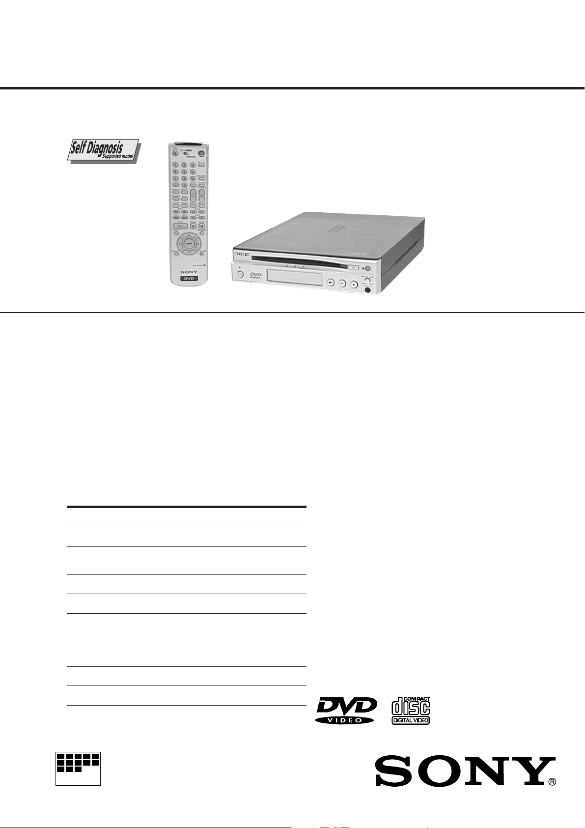
DVP-F11
RMT-D109E/D109O
SERVICE MANUAL
SPECIFICATIONS
CD/DVD player
Laser Semiconductor laser
Signal format system PAL/(NTSC)
Audio characteristics
Frequency response DVD (PCM 96 kHz): 2 Hz to 44 kHz
(±1 dB)*
DVD (PCM 48 kHz): 2 Hz to 22 kHz
(±0.5 dB)
CD: 2 Hz to 20 kHz (±0.5 dB)
Signal-to-noise ratio More than 110 dB (LINE OUT (AUDIO
1, 2) connectors only)
Harmonic distortion Less than 0.0025%
Dynamic range More than 100 dB (DVD)
More than 97 dB (CD)
Wow and flutter Less than detected value
(±0.001% W PEAK)
Outputs and inputs
Jack Output Load impedance
type level
LINE OUT Phono 2 Vrms Over 10 kilohms
(AUDIO1, 2) jacks (at 50 kilohms)
OPTICAL Optical –18 dBm Wave length: 660 nm
output
connector
COAXIAL Phono 0.5 Vp-p 75 ohms terminated
jack
LINE OUT Phono 1.0 Vp-p 75 ohms,
(VIDEO1, 2) jacks sync negative
LINE OUT 4-pin Y: 1.0 Vp-p 75 ohms,
(S-VIDEO1, 2) mini DIN sync negative
C: 0.3 Vp-p 75 ohms terminated
(PAL)
0.286 Vp-p
(NTSC)
LINE OUT Phono 2 Vrms Over 10 kilohms
(WOOFER OUT) jacks
PHONES Phone 12 mW 32 ohms
jack
AEP Model
UK Model
E Model
Hong K ong Model
Singapore Model
Australian Model
Chinese Model
General
Power requirements DC 10.5 V
Power consumption 13 W
Dimensions (approx.) 215 × 60 × 314 mm (w/h/d)
incl. projecting parts
Mass (approx.) 2.1 kg
Operating temperature 5°C to 35°C
Operating humidity 25% to 80%
AC power adaptor
Power requirements 220 to 240 V AC, 50/60 Hz
Power consumption 19 W
Output voltage DC 10.5 V, 1.3 A in operating mode
Dimensions (approx.) 125 × 39 × 62 mm (w/h/d)
excl. projecting parts
Mass (approx.) 235 g
Operating temperature 5°C to 35°C
Storage temperature –20°C to +60°C
Supplied accessories
• Audio/Video connecting cord (1)
• S video cord (1)
• AC power adaptor AC-F11 (1)
• AC power cord (1)
• Remote commander (remote) RMT-D109O (1)
(Except Hong Kong, Singapore and Chinese)
Remote commander (remote) RMT-D109E (1)
(Hong Kong, Singapore and Chinese)
• Size AA (R6) batteries (2)
• Stand (1)
• EURO AV adaptor (1)
(Except Hong Kong, Singapore, Australian and Chinese)
* The signals from LINE OUT (AUDIO1, 2) connectors are measured.
When you play the PCM sound tracks with 96 kHz sampling frequency,
the output signals from the OPTICAL and COAXIAL connectors are
converted to 48 kHz (sampling frequency).
Design and specifications are subject to change without notice.
MICROFILM
CD/DVD PLAYER
Page 2
WARNING!!
WHEN SERVICING, DO NO T APPR O A CH THE LASER
EXIT WITH THE EYE TOO CLOSELY. IN CASE IT IS
NECESSARY TO CONFIRM LASER BEAM EMISSION,
BE SURE TO OBSERVE FROM A DISTANCE OF
MORE THAN 25 cm FROM THE SURFACE OF THE
OBJECTIVE LENS ON THE OPTICAL PICK-UP BLOCK.
CAUTION:
The use of optical instrument with this product will increase eye
hazard.
CAUTION
Use of controls or adjustments or performance of procedures
other than those specified herein may result in hazardous radiation exposure.
CLASS 3B LASER
LUOKAN 3B LASER
LASERKLASS 3B
SAFETY CHECK-OUT
After correcting the original service problem, perform the following
safety checks before releasing the set to the customer:
1. Check the area of your repair for unsoldered or poorly-soldered connections. Check the entire board surface for solder
splashes and bridges.
2. Check the interboard wiring to ensure that no wires are
“pinched” or contact high-wattage resistors.
3. Look for unauthorized replacement parts, particularly transistors, that were installed during a previous repair. Point them
out to the customer and recommend their replacement.
SAFETY-RELATED COMPONENT WARNING!!
COMPONENTS IDENTIFIED BY MARK 0 OR DOTTED
LINE WITH MARK 0 ON THE SCHEMATIC DIAGRAMS
AND IN THE PARTS LIST ARE CRITICAL TO SAFE
OPERATION. REPLACE THESE COMPONENTS WITH
SONY PARTS WHOSE PART NUMBERS APPEAR AS
SHOWN IN THIS MANUAL OR IN SUPPLEMENTS PUBLISHED BY SONY.
4. Look for parts which, though functioning, show ob vious signs
of deterioration. Point them out to the customer and recommend their replacement.
5. Check the B+ voltage to see it is at the values specified.
– 2 –
Page 3

TABLE OF CONTENTS
Section Title Page Section Title Page
Service Note ............................................................................ 4
1. GENERAL
This Player Can Play the Following Discs .................... 1-1
Getting Started .............................................................. 1-2
Playing Discs ................................................................. 1-4
Using Var ious Functions with the Control Menu ........... 1-6
Settings and Adjustments ............................................. 1-10
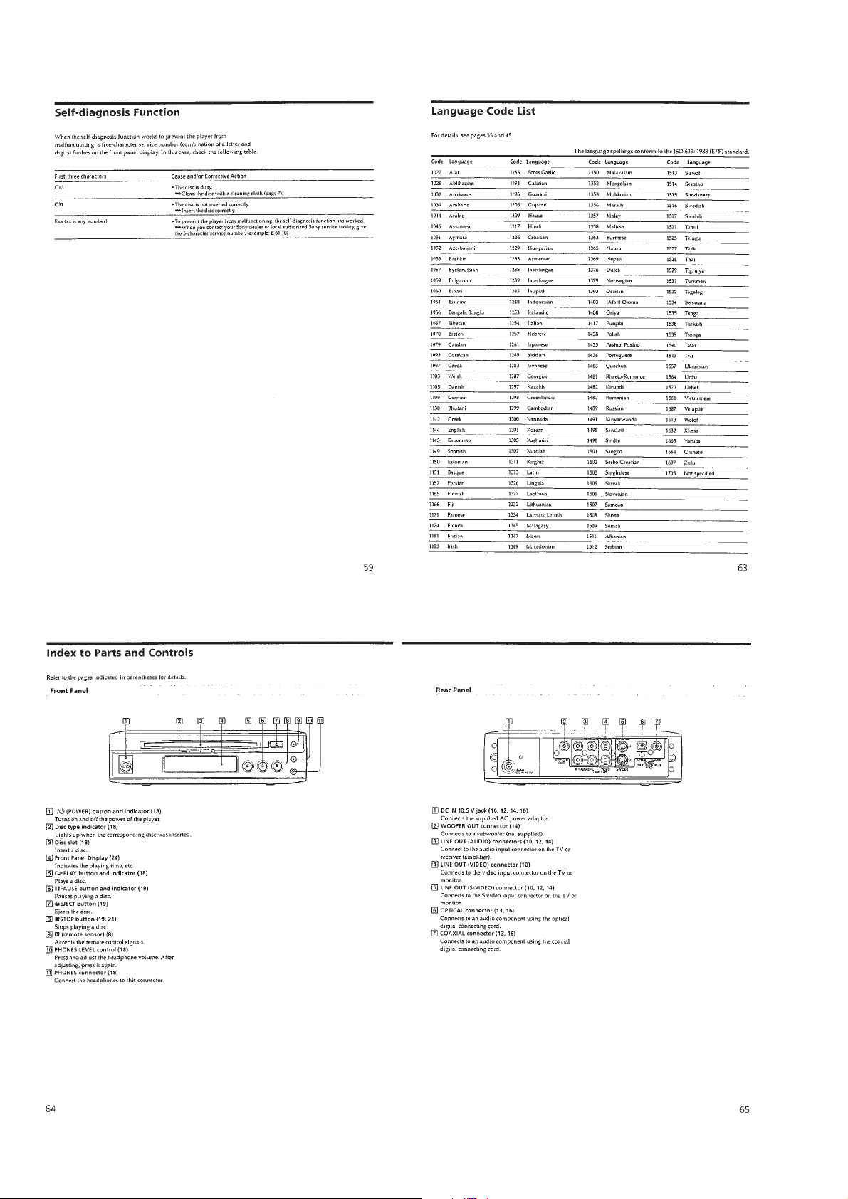
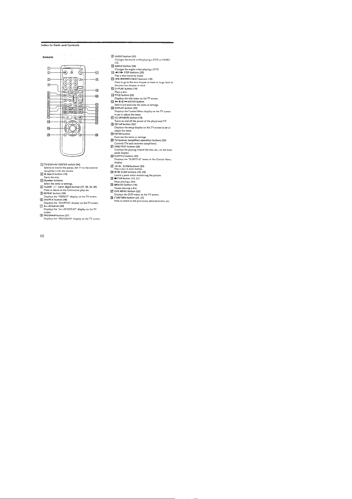
Index to Parts and Controls .......................................... 1-14
2. DISASSEMBLY
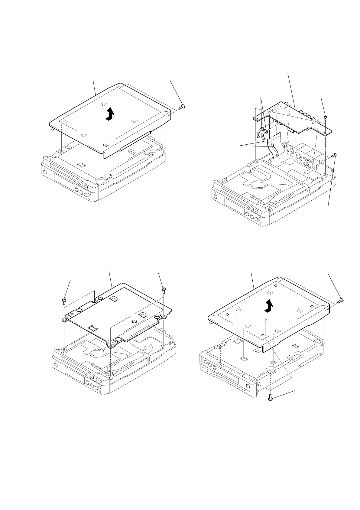
2-1. Case (Upper) Removal ................................................. 2-1
2-2. Chassis (Upper) Removal ............................................. 2-1
2-3. AU-222 Board Removal ................................................ 2-1
2-4. Case (Lower) Removal.................................................. 2-1
2-5. Rear Panel, MB-85 Board Removal.............................. 2-2
2-6. DC-DC Converter Unit Removal ................................... 2-2
2-7. Front Panel Section Removal........................................ 2-2
2-8. MD Block Ass’y Removal .............................................. 2-2
2-9. TK-55 Board, Optical Pick-up Removal ........................ 2-3
2-10. Chassis (Top) Block Ass’y, Chucking Arm Ass’y
Removal......................................................................... 2-3
2-11. Cam Slider, Chassis (Front) Block Ass’y Removal....... 2-3
2-12. Roller Arm Block Ass’y, LD Motor Ass’y Removal........ 2-3
2-13. Internal Views................................................................ 2-4
2-14. Circuit Boards Location................................................. 2-5
3. BLOCK DIAGRAMS
3-1. Overall Block Diagram................................................... 3-1
3-2. RF/Servo Block Diagram............................................... 3-3
3-3. Signal Process/Video Block Diagram ........................... 3-5
3-4. System Control Block Diagram ..................................... 3-7
3-5. Audio (1) Block Diagram ............................................... 3-9
3-6. Audio (2) Block Diagram ............................................... 3-11
3-7. Interface Control Block Diagram ................................... 3-13
3-8. Power Block Diagram.................................................... 3-15
4. PRINTED WIRING BOARDS AND SCHEMATIC
DIAGRAMS
HP-122 Printed Wiring Board
and Schematic Diagram................................................ 4-55
MPD0102 Printed Wiring Board
and Schematic Diagram................................................ 4-57
5. IC PIN FUNCTION DESCRIPTION
5-1. System Control Pin Function
(MB-85 Board IC202) .................................................... 5-1
6. TEST MODE
6-1. General Description ...................................................... 6-1
6-2. Starting Test Mode ........................................................ 6-1
6-3. Syscon Diagnosis.......................................................... 6-1
6-4. Drive Auto Adjustment .................................................. 6-5
6-5. Drive Manual Operation ................................................ 6-7
6-6. Mecha Aging ................................................................. 6-9
6-7. Emergency History ........................................................ 6-9
6-8. Version Information ....................................................... 6-10
6-9. Video Level Adjustment ................................................ 6-10
6-10. If Con Self Diagnostic Function .................................... 6-11
7. ELECTRICAL ADJUSTMENTS
7-1. Power Supply Adjustment ............................................. 7-1
1. MPD0102 BOARD......................................................... 7-1
7-2. Adjustment of Video System......................................... 7-2
1. Video Level Adjustment (MB-85 BOARD) .................... 7-2
2. S-terminal Output Check (MB-85 BOARD) .................. 7-2
3. Checking S Video Output S-C (MB-85 BOARD) .......... 7-2
7-3. Adjustment Related Parts Arrangement ....................... 7-4
8. REPAIR PARTS LIST
8-1. Exploded Views ............................................................. 8-1
8-1-1. Case and Front Panel Assemblies ........................... 8-1
8-1-2. Chassis Assembly .................................................... 8-2
8-1-3. Mechanism Deck Assembly-1.................................. 8-3
8-1-4. Mechanism Deck Assembly-2.................................. 8-4
8-2. Electrical Parts List ....................................................... 8-5
4-1. Frame Schematic Diagram ............................................ 4-3
Frame (1) Schematic Diagram...................................... 4-3
Frame (2) Schematic Diagram...................................... 4-5
4-2. Printed Wiring Boards and Schematic Diagrams ......... 4-7
TK-55 Printed Wiring Board .......................................... 4-7
TK-55 Schematic Diagram ............................................ 4-11
SW-332 Printed Wiring Board
and Schematic Diagram................................................ 4-13
MB-85 Printed Wiring Board ......................................... 4-15
MB-85 (AV DECODER) Schematic Diagram................ 4-19
MB-85 (SDRAM) Schematic Diagram .......................... 4-21
MB-85 (SERVO DSP) Schematic Diagram................... 4-23
MB-85 (DRIVE) Schematic Diagram ............................ 4-25
MB-85 (ARP) Schematic Diagram ................................ 4-27
MB-85 (SYSTEM CONTROL) Schematic Diagram...... 4-29
MB-85 (HGA) Schematic Diagram................................ 4-31
MB-85 (CLOCK GENERATOR/AUDIO DSP)
Schematic Diagram ....................................................... 4-33
MB-85 (DAC) Schematic Diagram ................................ 4-35
MB-85 (BIAS) Schematic Diagram ............................... 4-37
AU-222 Printed Wiring Board........................................ 4-39
AU-222 (AUDIO) Schematic Diagram ........................... 4-43
AU-222 (VIDEO BUFFER) Schematic Diagram ........... 4-45
FL-111 Printed Wiring Board ........................................ 4-47
FL-111 Schematic Diagram .......................................... 4-49
FR-166 Printed Wiring Board........................................ 4-51
FR-166 Schematic Diagram.......................................... 4-53
– 3 –
Page 4
SERVICE NOTE
1. DISASSEMBLY
• This set can be disassembled in the order shown below.
Note on Replacing IC601 (IF CON) (FL-111 Board)
Set
Case (Upper)
(Page 2-1)
Chassis(Upper)
(Page 2-1)
AU-222 Board
(Page 2-1)
Case (Lower)
(Page 2-1)
Rear Panel
(Page 2-2)
Case (Lower)
(Page 2-1)
Front Panel
Section
(Page 2-2)
MD Block
Ass’y
(Page 2-2)
TK-55 Board
(Page 2-3)
Optical
Pick-up
(Page 2-3)
Chassis (Top)
Block Ass’y
(Page 2-3)
Cam Slider
(Page 2-3)
Chucking
Arm Ass’y
(Page 2-3)
There are two types of IC601 (IF CON).
Version Type (Par t No.)
Ver. 1.00 M38B57MCH-E227FP (8-759-599-87)
Ver. 1.01 M38B57MCH-D233FP (8-759-658-36)
• Version checking method
Type
When replacing the IC601, always check the version of old part
and new part. If different, follo w the “description of replacement”
given below.
Old part New part
(Ver.) (Ver.)
Description of replacement
Replace as it is. (However, for the CED
Model (serial No. 800001-800100), also
1.00
1.00
replace the resistor R659 47 k (1-216089-00) with 1.5 k (1-216-053-00), and
further remove the resistors R653, 654,
661, 662, 663, 664.)
Replace as it is. (However, for the CED
1.01
Model (serial No. 800001-800100), also
remove the resistors R653, 654, 661,
662, 663, 664.)
Also, replace resistor R659 47 k (1-216089-00) with 1.5 k (1-216-053-00).
1.01
1.00
1.01 Replace as it is.
MB-85 Board
(Page 2-2)
DC-DC CON-
VERTER UNIT
(Page 2-2)
Chassis (Front)
Ass’y
(Page 2-3)
Roller Arm
Block Ass’y
(Page 2-3)
LD Motor
Ass’y
(Page 2-3)
– 4 –
Page 5
SECTION 1
GENERAL
DVP-F11
This section is extracted from instruction manual (3-867-780-11).
1-1
Page 6
1-2
Page 7
1-3
Page 8
1-4
Page 9
1-5
Page 10
1-6
Page 11
1-7
Page 12
1-8
Page 13
1-9
Page 14
1-10
Page 15
1-11
Page 16
1-12
Page 17
1-13
Page 18
1-14
Page 19
1-15 E
1-15
Page 20
SECTION 2
1 Two screws
(B3)
2 Four screws
(B3)
3 Remove the case (lower)
in the direction of the arrow.
DISASSEMBLY
Note: Follow the disassembly procedure in the numerical order given.
2-1. CASE (UPPER) REMOVAL 2-3. AU-222 BOARD REMOVAL
DVP-F11
2 Remove the case (upper)
in the direction of the arrow.
1 Two screws
(B3)
5 Two flat cables
(CN301, 302)
4 AU-222 board
1 Two connectors
(CN303, 306)
3 Two screws
(B3) (ring)
2 Five screws
(B3)
2-2. CHASSIS (UPPER) REMOVAL 2-4. CASE (LOWER) REMOVAL
2 Two screws
(B3)
1 Two screws
(B3)
3 Chassis (upper)
2-1
Page 21
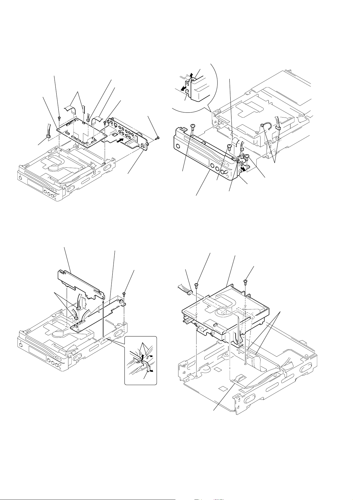
2-5. REAR PANEL, MB-85 BOARD
(
)
REMOVAL
2-7. FRONT PANEL SECTION REMOVAL
8 Two screws
(B3) (ring)
9 MB-85 board
3 Connector
(CN001)
4 Three flat cables
(CN002, 003, 009)
5 Connector
(CN011)
6 Flat cable
(CN006)
7 Two screws
2 Rear panel
(B3) (ring)
1 Two screws
(B3)
8 Claw
6 Screw
9 Boss
(B3) (ring) 5 Screw
0 Front panel section
1 Flat cable
4 Screw
(B3)
(CN602)
7 Claw
2 Connector
CN501
3 Two connectors
(B3) (ring)
(CN102, 203)
2-6. DC-DC CONVERTER UNIT REMOVAL 2-8. MD BLOCK ASS’Y REMOVAL
3 Heat insulating plate
4 Two connectors
(CN201, 203)
6 DC-DC converter unit
5 Four screws
(B3) (ring)
1 Harness
2 Claw
6 Connector
(CN005)
2 Three screws
(B3)
1 Flat cable
(CN101)
4 MD block ass’y
3 Screw
(B3)
5 Two flat cables
(CN003, 004)
2-2
Page 22
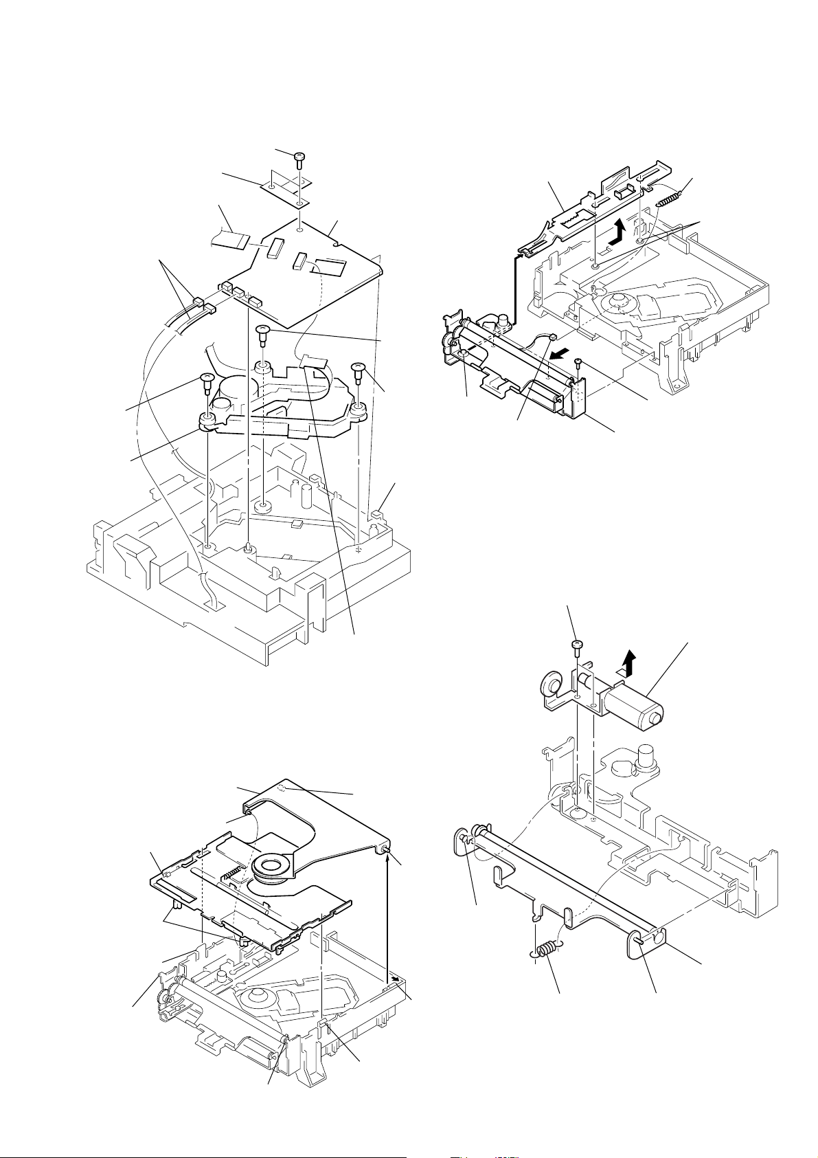
2-9. TK-55 BOARD, OPTICAL PICK-UP
5 Connector
(CN006)
3 Shaft
2 Two shafts
1 Tension spring
(cam slider)
4 Remove the cam slider in the
direction of the arrow A.
6 Three screws
(P2.6 × 6)
7 Chassis (front) block ass’y
A
REMOVAL
1 Two screws
(B3)
2 Ground plate (MD)
2-11. CAM SLIDER, CHASSIS (FRONT)
BLOCK ASS’Y REMOVAL
3 Flexible board
5 Two connectors
(CN006, 007)
q; Screw
qa Optical
pick-up
(CN002)
7 TK-55
board
9 Screw
8 Screw
6 Claw
2-12. ROLLER ARM BLOCK ASS’Y,
LD MOTOR ASS’Y REMOVAL
5 Two screws
(M1.7)
2-10. CHASSIS (TOP) BLOCK ASS’Y,
CHUCKING ARM ASS’Y REMOVAL
qa Chucking arm ass’y
6 Chassis (top)
block ass’y
5 Open the
centering lever.
2 Claw
4 Claw
q; Shaft
4 Flexible board
(CN001)
9 Shaft
8 Shaft
7 Claw
3 Shaft
1 Tension spring
(roller)
6 LD motor ass’y
4 Roller arm
block ass’y
2 Shaft
3 Claw
1 Claw
2-3
Page 23
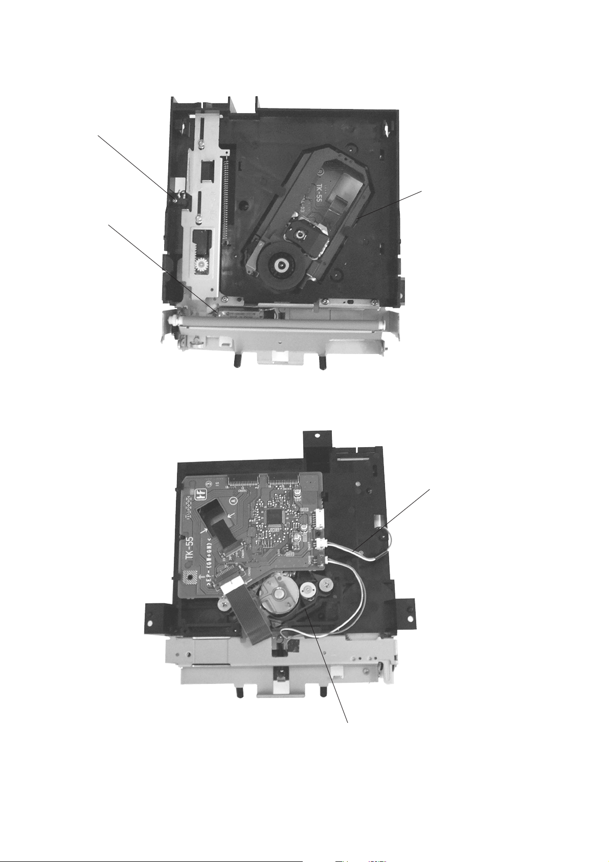
2-13. INTERNAL VIEWS
Switch (chuck sensor)
1-570-771-21
LD motor ass’y
(loading)
A-6062-252-A
Optical pick-up
(KHM-220AAA/J1RP)
8-820-081-09
Optical pick-up
(KHM-220AAA/J1RP)
8-820-081-09
Harness (ST-117)
1-960-020-11
2-4
Page 24

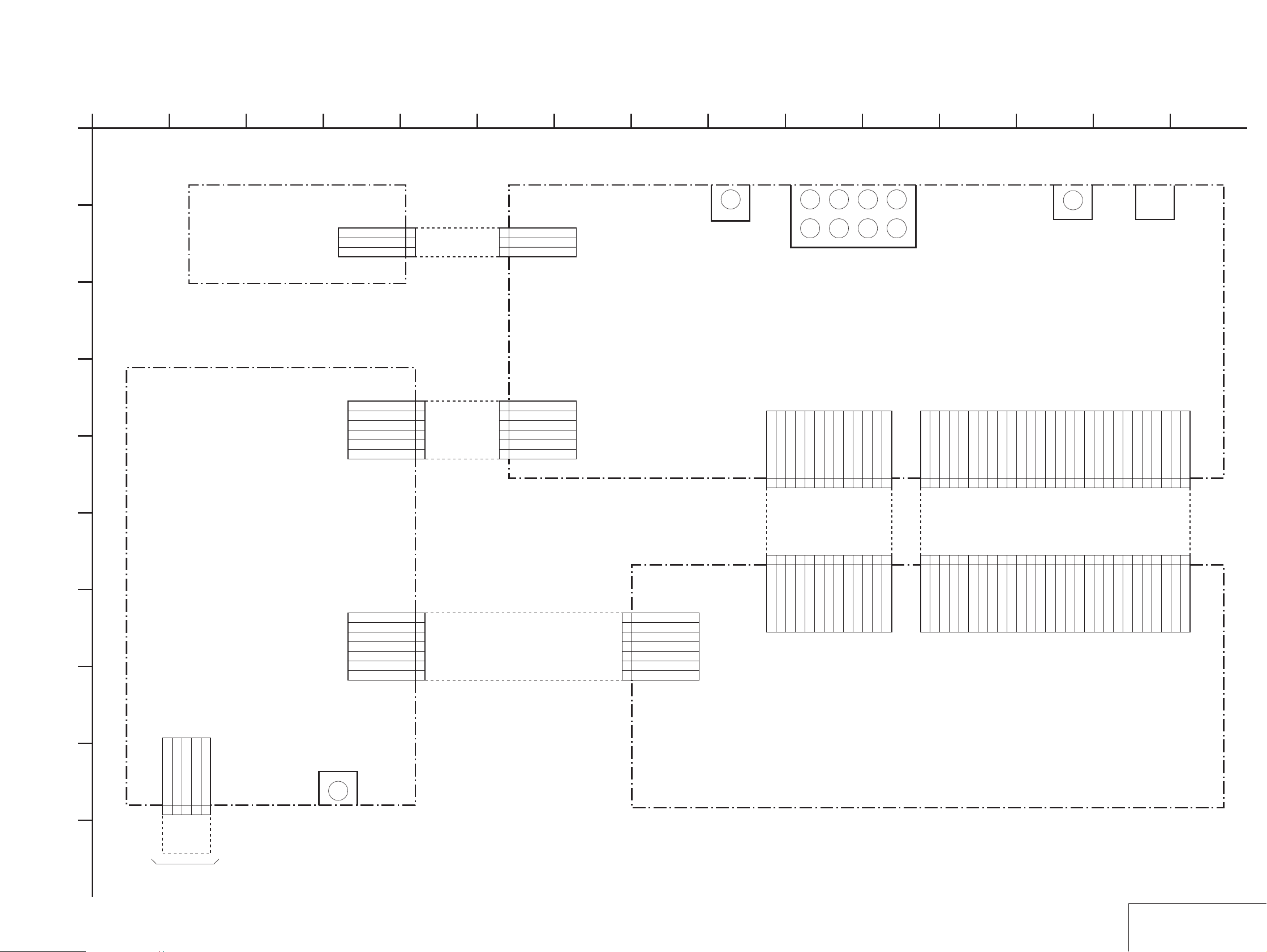
2-14. CIRCUIT BOARDS LOCATION
MB-85
(SIGNAL PROCESS/SERVO)
TK-55
(RF/SERVO)
FR-166
(IR/FUNCTION SWITCH)
SW-332
(CHUCK SENSOR)
AU-222
(AUDIO)
DC-DC Converter Unit
(SWITCHING REGULATOR)
FL-111
(IF CON)
HP-122
(HEAD PHONE)
2-5 E
2-5
Page 25
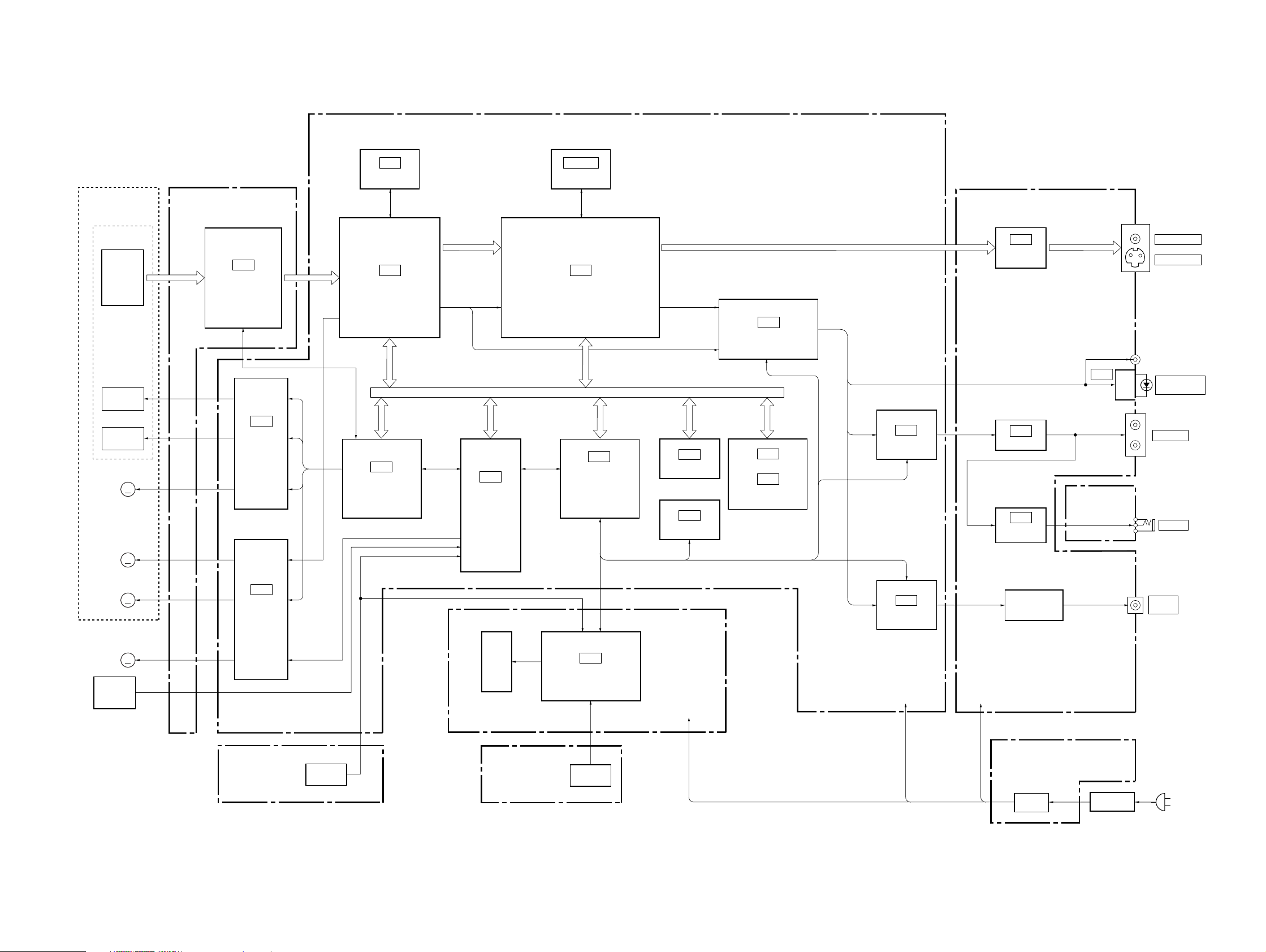
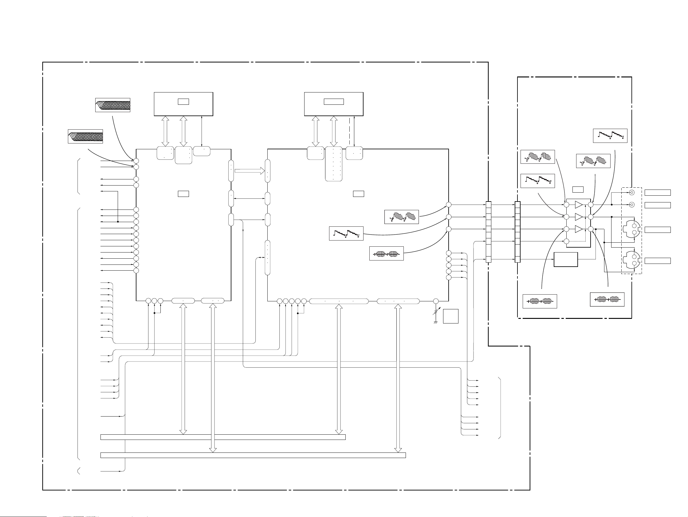
3-1. OVERALL BLOCK DIAGRAM
SECTION 3
BLOCK DIAGRAMS
MB-85 BOARD
(SEE PAGE 4-19 to 37)
DVP-F11
BASE UNIT
KHM-220AAA
OPTICAL DEVICE
DVD/CD
FOCUS
TRACKING
TILT
MOTOR
SPINDLE
MOTOR
PDIC
COIL
COIL
IC304
16M DRAM
TK-55 BOARD
(SEE PAGE 4-11)
SD 0-7
RF
IC001
DVD/CD RF AMP
DIGITAL SERVO
IC801
FOCUS COIL/
TRACKING COIL/
TILT MOTOR
DRIVE
M
DVD RF,
CD RF
IC303
ARP2
IC701
SERVO DSP
CDDOUT, CDDATA,
CDBCK, CDLRCK
IC601
HGA
M
IC402, 403
16M SDRAM
IC401
AV DECODER
IC202
SYSTEM CONTROL
Parallel BUS
Serial BUS
ACH12,
ACH34, ACH56,
BCK, LRCK
IC204
1M SRAM
IC201
4K EEP ROM
IC501
AUDIO DSP
IC205
:EXCEPT CED, UK, Chinese
IC206
:CED, UK, Chinese
16M FLASH
VIDEO V,
VIDEO Y,
VIDEO C
SPDIF
IC902
AUDIO 2CH DAC
AU-222 BOARD
(SEE PAGE 4-43, 45)
AUDIO LT,
AUDIO RT
HEADPHONE
IC308
VIDEO
BUFFER
IC303
LPF
IC307
AMP
IC309
HP-122 BOARD
(SEE PAGE 4-55)
VIDEO 1, 2
S VIDEO 1, 2
PCM/DTS/
DOLBY DIGITAL
AUDIO 1, 2
PHONES
SLED
MOTOR
M001
LOADING
MOTOR
CHUCK
SENSOR
S001
M
M
05
IC802
SPINDLE/SLED/
LOADING
MOTOR DRIVE
SW-332 BOARD
(SEE PAGE 4-14)
SWITCH
ND601
FL-111 BOARD
(SEE PAGE 4-49)
FR-166 BOARD
(SEE PAGE 4-53)
IC601
IF CON
SWITCH
SW–10V
EVER5V
IC907
WOOFER DAC
SW+3.3V
SW+5V
SW+10V
MIX, LPF
SW+5V
SW+10V
SW–10V
EVER5V
DC-DC CONVERTER UNIT (MPD0102)
(SEE PAGE 4-57)
SW REG
AC ADAPTOR
WOOFER
OUT
3-1 3-2
Page 26
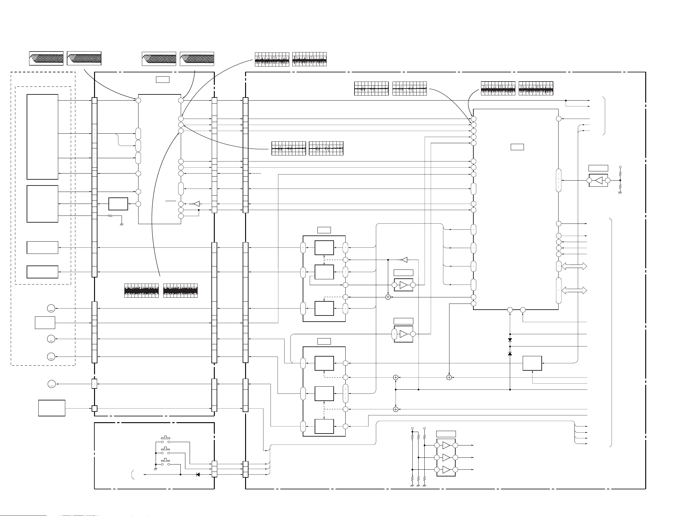
DVP-F11
3-2. RF/SERVO BLOCK DIAGRAM
200mV/DIV 100ns/DIV
BASE UNIT
KHM-220AAA
OPTICAL DEVICE
MOTOR
SPINDLE
MOTOR
LOADING
IC0011(DVD play)
536mVp-p
DVD/CD
PDIC
DVD/CD
LD MODULE
COIL
TRACKING
COIL
TILT
M
INLIMIT
SENSOR
M
SLED
M
MOTOR
M001
M
MOTOR
S001
CHUCK
SENSOR
IC0011(CD play)
500mV/DIV 500ns/DIV
880mVp-p
RF
7
9
A-D
10
16
17
8
E-H
11
15
18
VC
13
PD
4
LD
2
VR
5
FCSFOCUS
19
20
TRK
21
22
10
TIA, TIB
ı
13
INLIM
2
8
SPM
9
4
SLA, SLB
ı
7
LDM
1
2
OCSW2
1
05
TK-55 BOARD
CN001
CN002
CN006
CN007
SW-332 BOARD (1/2)
(SEE PAGE 4-14)
Q001
LD DRIVE
(SEE PAGE 4-11)
IC001wl(DVD play)
200mV/DIV 500ms/DIV
(CHUCK SENSOR)
INTERFACE
CONTROL
(SEE PAGE 3-13)
IC001tf(DVD play)
500mV/DIV 100ns/DIV
1.5Vp-p
IC001
DVD/CD RF AMP
DIGITAL SERVO
RF IP
1 54
9
ı
A-D
12
5
ı
A2-D2
8
13
E-H
ı
16
VC
17
19
PD
20
592mVp-p
S101-103
S101
LD
FDCHG
HOLD2
200mV/DIV 20ms/DIV
IC001tf(CD play)
500mV/DIV 500ns/DIV
SIGO
40
FE
39
TE
29
PI
26
MIRR
32
TZC
33
VCI
SCLK
43
SWD
ı
SRD
46
SDEN
27
42
31
DFT
IC001wl(CD play)
448mVp-p
S103
S102
S101
1.5Vp-p
Q002
CN004
CN005
CN101
17
9
8
7
3
5
6
SSCK, SSWD,
11
ı
14
15
4
6
7
4
5
15
ı
18
8
13
14
9
ı
12
1
2
6
4
3
2
RF+
FE
TE
PI
MIRR
TZC
2VC
SSRD, SSCS
SSDFCT
SSDFCTI
FCS
TRK
TIA, TIB
INLIM
SPM
SLA, SLB
LDM
OCSW2
OCSW1
CKSW2
CKSW1
IC001r;(DVD play)
100mV/DIV 50ms/DIV
180mVp-p
MB-85 BOARD (1/6)
(SEE PAGE 4-23, 25)
CN002CN003
2
10
11
12
500mV/DIV 50ms/DIV
16
14
13
15
12
13
14
15
11
10
5
ı
8
4
1
ı
4
5
6
7
ı
1
2
6
1
3
2
3
CN003
CN011
OCSW2
CN009
OCSW1
CKSW2
CKSW1
2VC
IC001r;(CD play)
500mV/DIV 50ms/DIV
IC001el(DVD play)
1.3Vp-p
860mVp-p
IC001el(CD play)
500mV/DIV 200ms/DIV
1.7Vp-p
IC801
FOCUS
13
14
11
12
15
18
15
16
11
14
17
18
COIL
DRIVE
TRACKING
COIL
DRIVE
ı
ı
TILT
MOTOR
DRIVE
IC802
SPINDLE
MOTOR
DRIVE
SLED
MOTOR
DRIVE
LOADING
MOTOR
DRIVE
IC701yl(DVD play)
500mV/DIV 50ms/DIV
2
3
9
5
6
7
20
TLTA, TLTB
23
26
26
20
2
SLDA, SLDB,
3
STVC
5
6
9
23
1.4Vp-p
FCD
TRD
IC701yl(CD play)
500mV/DIV 200ms/DIV
1.7Vp-p
Q801
IC702 (1/2)
3 1
IC803 (1/2)
12
13
+3.3V
14
+5V
IC803 (2/2)
5 7
10
3 1
FCD
TRD
TLTA,TLTB
SLDA, SLDB,
STVC
TILT MUTE
FGMODE
8
IC701yk(CD play)
500mV/DIV 50ms/DIV
68
ADC1
69
ADC0
67
ADC2
66
ADC3
65
ADC4
21
TRIN
20
TRREF
23
FGIN
41
GIO 5-8
ı
44
38
GIO 11
28
DFCTI
80
DAB 2, 3
85
92
DAB 0, 1
97
48
GIO 1, 2
49
7
PWM 0-2
ı
9
46
GIO 4
50
GIO 0
2.5VC
2VC
1.6VC
860mVp-p
IC701yk(DVD play)
100mV/DIV 5ms/DIV
IC701
SERVO DSP
RS
26 108
180mVp-p
X2/CLKIN
Q802, 803
GAIN
CONTROL
FG REF
VRBA,
VRB 0-3
GIO 10
HINT
HRD
HWR
HCS
EA 0, 1
HD 0-7
DVD RF
CD RF
SIGNAL PROCESS,
22
74
81
84
93
96
39
128
1
2
3
4
5
117
ı
120
122
ı
125
LOCK
MDS0
MDP0
IC702 (2/2)
7 5
FCSON
XSDPIT
XSDPRD
XSDPWR
XSDPCS
HA0, 1
HD8-15
N27MSDP
XSDPRST
X3VRST
SPDLSTOP
SPGAIN
XDRV MUTE
LDMM/DMM
LDMP/DMP
OCSW1
OCSW2
CKSW1
CKSW2
VIDEO
(SEE PAGE 3-5)
+3.3V
SYSTEM
CONTROL
(SEE PAGE 3-7, 8)
3-3 3-4
Page 27
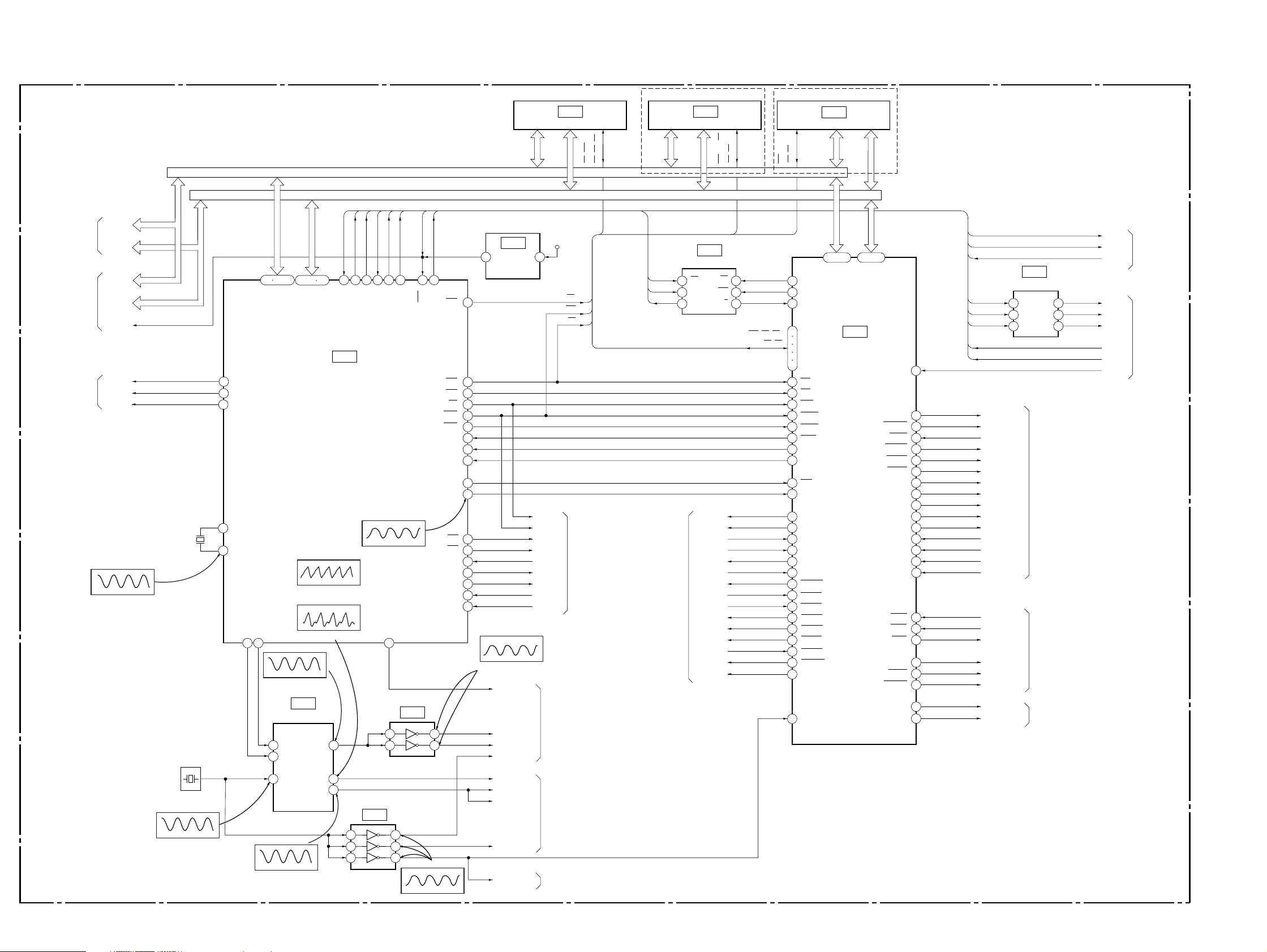
3-3. SIGNAL PROCESS/VIDEO BLOCK DIAGRAM
MB-85 BOARD (2/6)
(SEE PAGE 4-19, 21, 27, 35)
IC303qj(DVD play)
500mV/DIV 200ns/DIV
RF, SERVO
(SEE PAGE 3-4)
SYSTEM
CONTROL
(SEE PAGE 3-7, 8)
IC303ql(CD play)
1.6Vp-p
DVD RF
CD RF
MDS0
MDP0
LOCK
DFCT
NORF
LOCK
FWON
MD2
MUTE
XARPWR
XARPRD
XARPIT
XARPCS
XARPWT
XCS2
XCS3
XRD
XWRH
XAVDIT
XAVDWT
DACK0
DREQ0
DACK1
DREQ1
500mV/DIV 100ns/DIV
1.6Vp-p
136-139
141-144
RFIN1
RFIN2
MDS0
MDP0
DFCT
NORF
LOCK
FWON
MD2
MUTE
XWR
XRD
XINT
XCS
XWAT
XRST
87
121
XARPRST
33MARP
146 147
MCKI
123
17
19
49
52
55
56
58
59
113
111
60
61
83
84
86
MA 0-9
SCKI
IC304
16M DRAM
MD 00-15
154-157
159-162
164-167
169-172
IC303
ARP2
A 0-7
73-76 79-82
XRAS, XOE
XMWR, XCAS,
148
150-152
63-68 70 71
SD 0-7
D 0-7
97
SD 0-7
98
100
ı
105
SDCK, SDEF,
91
XSHD, XSAK, XSRQ
93
ı
96
CDDOUT, CDDATA,
107
CDBCK, CDLRCK
ı
110
DVP-F11
AU-222 BOARD (1/2)
(SEE PAGE 4-43, 45)
IC402, 403
16M SDRAM
IC308qg
DDT 0-15
DAD 0-11
105-108
110-113
CRPCLKI
160 163
27M30
33M30
115-118
SCLKIN
CLKI
168-170 172-178 180-187 189-192 2-5 7-10 12-15 205-208
38
ı
43
DT 0-7 I
45
46
47
ı
51
29
ı
32
166
167
193
194
196
198
ı
202
RSTIN
ACLKI
103 19 36
256FS30
XAVDRST
134 135
137 138
140 141
143 144
146 147
149 150
152 153
155 156
CLK, CKE,
DQML, DQMU,
120-123
125 127
129-132
AV DECODER
IC401ya
1.1Vp-p(H)
HAD 0-21 I
CS, WE, CAS, RAS
IC401
IC401ys
816mVp-p(H)
IC401yg
1.2Vp-p(H)
HD 0-15
COMP OUT
Y OUT
C OUT
ACH12O
ACH34O
ACH56O
LRCKO
BCKO
VREFI
70
65
61
62
21
22
23
25
26
RV401
VIDEO
LEVEL
ADJ
CN005
IC3084
1.2Vp-p(H)
IC3082
1.1Vp-p(H)
VIDEO V
1
VIDEO Y
3
VIDEO C
5
V MUTE
8
VS
6
CN301
28
26
24
21
23
IC3087
860mVp-p(H)
VIDEO BUFFER
4 13
2
7 10
1
Q323, 324
DC ON/OFF
IC308
IC308qd
2.4Vp-p(H)
15
2.0Vp-p(H)
IC3080
1.8Vp-p(H)
J302
Y
C
Y
C
VIDEO OUT1
VIDEO OUT2
S VIDEO OUT1
S VIDEO OUT2
INTERFACE
CONTROL
(SEE PAGE 3-14)
05
XARPRST
XAVDRST
33MARP
256FS30
33M30
27M30
VS
HA 0-21
HD 0-15
V MUTE
CDDOUT, CDDATA, CDBCK, CDLRCK
ACH12
ACH34
ACH56
LRCK
HA 0-7
HD 8-15
HA 0-21
HD 0-15
BCK
CDDOUT
CDDATA
CDBCK
CDLRCK
AUDIO 1
(SEE PAGE 3-9)
3-5 3-6
Page 28
DVP-F11
3-4. SYSTEM CONTROL BLOCK DIAGRAM
MB-85 BOARD (3/6)
(SEE PAGE 4-29, 31, 33)
SIGNAL PROCESS,
VIDEO
(SEE PAGE 3-5)
RF, SERVO
(SEE PAGE 3-4)
AUDIO 2
(SEE PAGE 3-11)
05
HA 0-21
HD 0-15
HA 0, 1
HD 8-15
X3VRST
GAIN2
VFC1
VFC2
IC202os
2.4Vp-p(12.5MHz)
X201
12.5MHz
X001
27MHz
IC0016
4.2Vp-p(27.0MHz)
HA 0-21
42 44-64
3
PB7
1
PB5
96
PB0
91
X1
92
X0
P66
PB4
66 100 98
CKSEL
DVD/CD
DVD:5.8Vp-p(36.5MHz)
CD:5.1Vp-p(33.8MHz)
19
1
6
4.6Vp-p(33.8MHz)
A 01-15
IC001qj
MD
ML
XT1
IC001qs
HD 0-15
25-39 41
D 16-31
SYSTEM CONTROL
IC001qf(DVD play)
4.2Vp-p(25.3MHz)
IC001qf(CDplay)
4.7Vp-p(22.5MHz)
IC001
PLL
SCKO3
17
14
SCKO2
12
SCKO1
SI0
SO0
SO0
3
6
1
SI1
SC0
SO1
SI1
SC0
SO1
IC2025
4Vp-p(25.3MHz)
PB2
1
3 5
IC004
5
2
7
SC1
SC1
IC003
IC0042,5,7
4.2Vp-p(26.9MHz)
SIO
76 77 78 79 80 89 14 97
IC202
CS0L
XFRRST
RST
7
PB1
WR0
WR1
INT1
INT3
DACK1
DACK0
DREQ1
DREQ0
CS0
CS1
CS4
RD
RDY
PF7
CLK
CS2
CS3
INT0
IC207
POWER ON
4 5
RESET
11
10
7
22
23
24
19
94
88
83
5
9
8
95
84
85
86
87
IC0035,7
DVD:6.2Vp-p(37.0MHz)
CD:5Vp-p(33.6MHz)
XDACS0
384FSDA
384FS01
27M01
256FS30
33MARP
33M30
27M30
N27MSDP
IC204
1M SRAM
HA 1-16
+3.3V
XRD
XWRH
XCS2
XCS3
XAVDIT
DACK1
DACK0
DREQ1
DREQ0
AUDIO 1
(SEE PAGE 3-9)
HD 0-15
CE
WE
CS
SIGNAL PROCESS,
VIDEO
(SEE PAGE 3-5)
RF, SERVO
(SEE PAGE 3-4)
CS, WE,
OE, UB, LB
SIGNAL PROCESS,
VIDEO
(SEE PAGE 3-5)
SIGNAL PROCESS,
VIDEO
(SEE PAGE 3-5)
EXCEPT CED, UK, Chinese
IC205
16M FLASH
HA 1-20
SC0
SO0
SI0
HD 0-15
IC201
4K EEPROM
4 3
SK
5 8
DI
DO
6 1
MUTE
NORF
DFCT
FWON
LOCK
XARPRST
XARPIT
XARPWT
XARPWR
XARPRD
XARPCS
XAVDWT
XAVDRST
N27MHGA
MD2
VS
WE, RY/BY,
CS
WC
R/B
OE, CE
WE, UB, LB,
RY/BY, OE
CED, UK, Chinese
WE,
OE, CE
23
XECS
24
XEWC
25
XEBSY
4
112
113
124
125
141
CS1
142
CS4
145
HRD
144
HWRH
143
HWRL
157
WAIT
156
HINT1
155
HINT3
3
RST
135
CPUCK
98
MUTE
99
MD2
102
NORF
103
DFCT
104
FWON
105
LOCK
106
ARPRST
107
ARPINT
108
ARPWT
109
ARPWR
110
ARPRD
111
ARPCS
72
AVDWT
71
AVDRST
53
VS
59
MCK
IC206
16M FLASH
HA 1-20
HA 0-5, 17-19
HA 0-5, 17-19
IC601
HGA
HD 0-15
HD 8-15
126-133146-154
HD 0-7
LDMM/DMM
XIFINT
FCSON
SDPRST
SDPIT
SDPWR
SDPRD
SDPCS
SPDLSTOP
SPGAIN
XDRVMUTE
LDMP/DMP
OCSW1
OCSW2
CKSW1
01IT0
01IT1
01CS
XDACS3
01RST
DACRST
EXPO0
MA MUTE
SC1
SO1
SI1
IC203
BUFFER
CS0L
12
SC0
SO0
SI0
XFRRST
22
54
114
115
116
117
118
57
94
93
92
91
64
63
88
83
29
30
28
97
31
26
55
49
4 6
1 3
FCSON
XSDPRST
XSDPIT
XSDPWR
XSDPRD
XSDPCS
SPDLSTOP
SPGAIN
XDRVMUTE
LDMP/DMP
LDMM/DMM
OCSW1
OCSW2
CKSW1
CKSW2CKSW2
X01INT0
X01INT1
X01CS
XDACS3
X01RST
XDACRST
SWSEL
MA MUTE
4A
4Y
2A
2Y
1A
1Y
RF, SERVO
(SEE PAGE 3-4)
AUDIO 1
(SEE PAGE 3-9)
AUDIO 2
(SEE PAGE 3-11)
11
SC1
SO1
SI1
XVIFCS
IFSC0
IFSO0
IFSI0
XFRRST
XIFINT
AUDIO 1
(SEE PAGE 3-9)
INTERFACE
CONTROL
(SEE PAGE 3-14)
3-7 3-8
Page 29
3-5. AUDIO (1) BLOCK DIAGRAM
MB-85 BOARD (4/6)
(SEE PAGE 4-33, 35)
DVP-F11
SIGNAL PROCESS,
VIDEO
(SEE PAGE 3-6)
SYSTEM CONTROL
(SEE PAGE 3-7, 8)
BCK
LRCK
ACH12
ACH34
ACH56
CDDOUT
CDDATA
CDBCK
CDLRCK
X01INT0
X01INT1
X01CS
SI1
SO1
SC1
XDACS0
XDACS3
X01RST
XDACRST
SO1
SC1
CS0
CS3
SO1
SC1
IC501
AUDIO DSP
47 9
BCKI
49 10
LRCKI
52 11
CH12I
51
CH34I
50
CH56I
25
CDDOBYP
26
CDSOBYP
27
CDBKCKI
28
CDLRCKI
55
CPU INT0
56
CPU INT1
61
SI
62
CS
63
SO
66
SCK
CLK
ACKI
RST
33 7 68
DO
BCKO
LRCKO
CH78O
CH56O
16
3
1
SO1
SC1
12
CS0
SO1
SC1
CS3
2
26
27
28
3
1
2
26
27
28
AUDIO 2CH DAC
BCLKIN
LRCIN
D IN
MD
MC
ML
WOOFER DAC
BCLKIN
LRCIN
D IN
MD
MC
ML
IC902
RSTB
522
IC907
RSTB
522
XTI
XTI
V OUT L
V OUT R
ZERO
ZEROR
V OUT R
ZEROR
16
13
21
17
13
17
SPDIF
AUDIOLT
AUDIORT
ZFLT
ZFRT
AUDIOLFE
ZFLFE
AUDIO 2
(SEE PAGE 3-11)
384FS01
27M01
384FSDA
05
3-9 3-10
Page 30
DVP-F11
3-6. AUDIO (2) BLOCK DIAGRAM
MB-85 BOARD (5/6)
(SEE PAGE 4-35)
INTERFACE
CONTROL
(SEE PAGE 3-14)
SYSTEM CONTROL
(SEE PAGE 3-7, 8)
AUDIO 1
(SEE PAGE 3-10)
A MUTE
MA MUTE
VFC2
VFC1
GAIN2
SWSEL
SPDIF
AUDIOLT
AUDIORT
ZFLT
ZFRT
CN005
CN007
IC309
1
D IN
CN306
J301
J302
COAXIAL
PCM/DTS/
DOLBY DIGITAL
OPTICAL
L
AUDIO OUT1
R
L
AUDIO OUT2
R
HP-122 BOARD
(SEE PAGE 4-55)
HPL
1
HPR
3
CN501
1
3
RV501
PHONES LEVEL
J501
PHONES
AU-222 BOARD (2/2)
(SEE PAGE 4-43, 45)
EXCEPT
Hong Kong, Singapore, Australian
IC303
LPF +6dB
3 1
5
Q311, 314
GAIN
7
CONTROL
IC305
MIX, LPF
3 1
6
Q317, 318
MUTE
IC307
HEADPHONE AMP
3
5
9
B
10
A
IC306
VARIABLE FC
CONTROL
1
Y0
2
Y2
Y3
4
7
14
18
16
19
10
20
22
11
1
13
CN301
CN302
Q306
Q304
Q303, 307
LEVEL SHIFT
Q326
Q327
SPDIF
15
AUDIOLT
11
AUDIORT
13
ZFLT
10
ZFRT
19
A MUTE
9
MA MUTE
7
VFC2
18
VFC1
28
GAIN2
1
Q325
BUFFER
Chinese,
Q330-333
FNAC
MUTE
1
7
Q321, 322
MUTE
3
Y
SWSEL
11
AUDIOLFE
AUDIOLFE
ZFLFE
05
9
ZFLFE
12
3
IC304
BUFFER, LPF+16dB
3 1
5
2
Q305
Q301, 302
MUTE CONTROL
5
7
Q319
LFE
MUTE
7
6
5
IC310
SELECTOR
J303
1
Q320
WOOFER
MUTE
WOOFER
OUT
3-11 3-12
Page 31

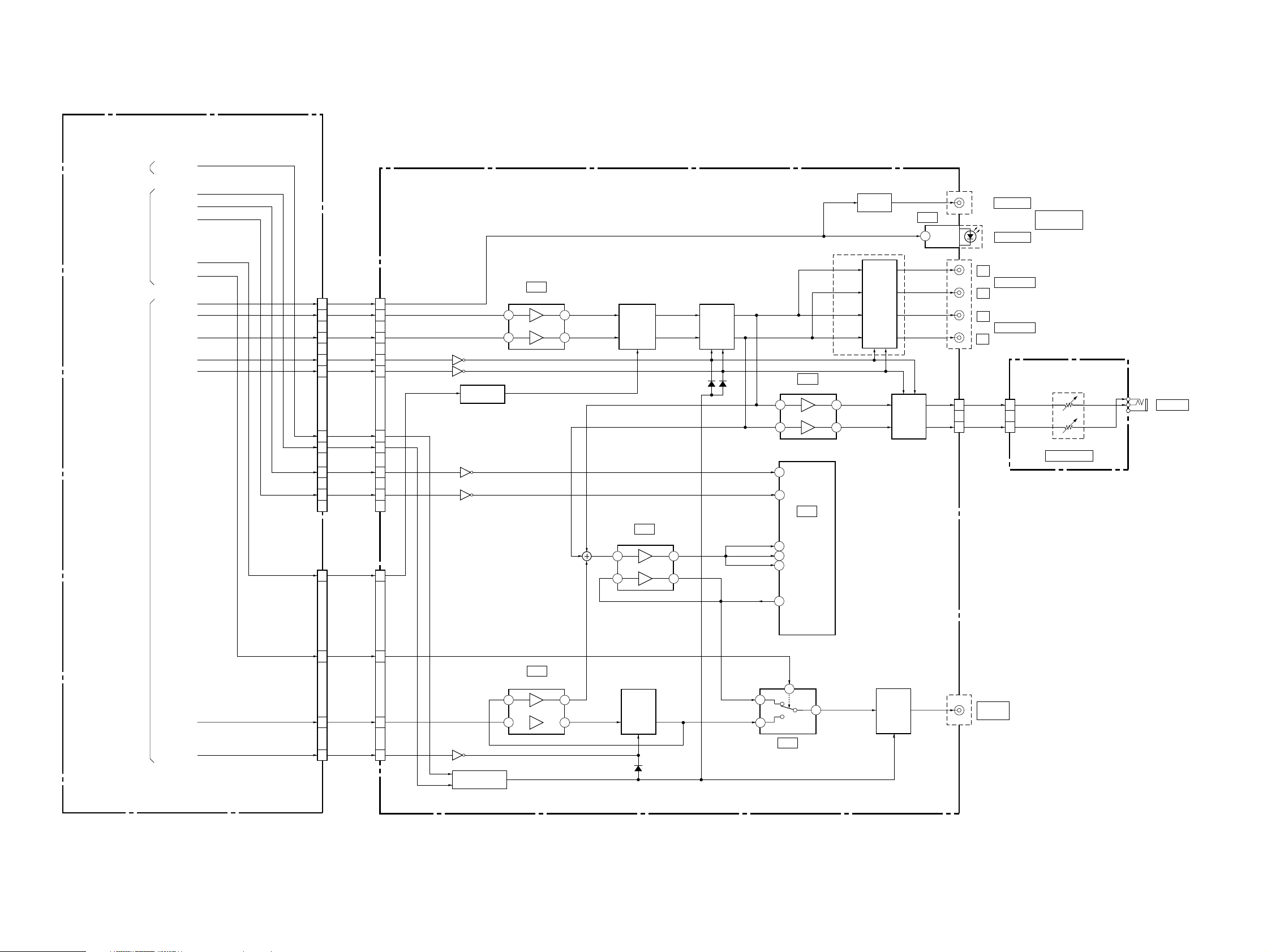
3-7. INTERFACE CONTROL BLOCK DIAGRAM
DVP-F11
FR-166 BOARD
(SEE PAGE 4-53)
D702
DVD
D701
(ON/STANDBY)
D703
VIDEO CD
D704
CD
IC701
REMOTE
COMMANDER
RECEIVER
OUT
1
CN701
FL-111 BOARD
(SEE PAGE 4-49)
CN603
IR
9
8
7
5
4
3
2
1
10
LPOW
LSTBY
LDVD
LVCD
LCD
LPAUSE
LPLAY
BT
9
8
7
IC602
POWER-ON RESET
4
V OUT
5
4
3
2
1
10
9
31
32
10
27
26
25
29
30
6
IR
L POWER
L STBY
RESET <N>
L DVD
L VCD
L CD
L PAUSE
L PLAY
AN0
IC601
IF CON
SCLK1
SOUT1
SIN1
SBUSY1
SRDY1
P CHECK<N>
FRRST <N>
V MUTE
A MUTE <N>
X IN
X OUT
70
71
72
76
78
77
8
11
12
14
15
X601
4MHz
IC601qf
3.9Vp-p(4MHz)
CN602
SC0
10
SI0
12
SO0
11
XIFCS
13
XIFBUSY
14
+3.3V
115
XFRRST
15
V MUTE
8
A MUTE
7
MB-85 BOARD (6/6)
(SEE PAGE 4-29)
CN006
6
4
5
3
2
1
8
9
+5V
+3.3V
IFSC0
IFSI0
IFSO0
XVIFCS
XIFINT
XFRRST
V MUTE
A MUTE
SYSTEM CONTROL
(SEE PAGE 3-8)
SIGNAL PROCESS, VIDEO
(SEE PAGE 3-5)
AUDIO 2
(SEE PAGE 3-11)
S702S701 S703 S704 S705
41
DIG1-8
D705
05
D706
SW-332 BOARD (2/2)
(SEE PAGE 4-14)
RF, SERVO
(SEE PAGE 3-3)
S101
CN102
2
CN604
FLD0
64
S101
2
ı
48
33
ı
SEG1-18
40
49
ı
58
13
ı
20
4
ı
11
22
ı
29
31
32
ND601
VACUUM
FLUORECENT
DISPLAY
3-13 3-14
Page 32

DVP-F11
3-8. POWER BLOCK DIAGRAM
AC ADAPTOR
(AC-F11)
FL-111 BOARD
(SEE PAGE 4-49)
IC601
DC-DC CONVERTER UNIT (MPD0102)
(SEE PAGE 4-57)
J201
ND601
IC602
LINE FILTER
Q201, 221
SWITCH
L202
T201
F1
F2
VEE
EVER5V
PCONT
FR-166 BOARD
(SEE PAGE 4-53)
IC281
EVER+5V REG
Q291, 293
B+ SWITCH
IC251
SW+5V REG
Q292, 294
POWER
CONTROL
IC701
Q604, 605
DC-DC
CONVERTER
CN701
T601
11
CN603
11
EVER5V
CN202
CN201
CN203
B601
1
4
2
6
1
2
5
6
7
2
4
1
4
2
1
EVER5V
SW+10V
SW+5V
SW–10V
SW+10V
SW+5V
SW+3.3V
EVER5V
SW–10V
PCONT
SW–10V
EVER5V
PCONT
SW+5V
SW+3.3V
SW+10V
SW+10V
SW–10V
SW+5V
EVER5V
MB-85 BOARD
(SEE PAGE 4-19 to 37)
CN001
+5V
5
+3.3V
6
7
V3.3V
1
2
CN006
15
+3.3V
AU-222 BOARD
(SEE PAGE 4-43, 45)
CN303
4
+7.5V/–7.5V
6
2
EVER5V
1
IC404
+3.3 REG
IC904
A+5V REG
IC801
IC802
IC301
IC308
IC309
A+5V
REG
IC401
+7.5V
–7.5V
IC902
IC907
IC303
IC304
IC305
IC307
IC306
IC310
IC302
+3.3 REG
IC203
IC702
IC803
+3.3 REG
IC005
IC303
IC001
IC003
IC004
CN002
IC201
IC202
IC204
IC207
IC304
IC402
IC403
IC501
IC601
IC701
IC205
EXCEPT CED, UK,
Chinese
IC206
CED, UK, Chinese
TK-55 BOARD
(SEE PAGE 4-11)
CN003
+5V
+3.3V
1
18
910
IC001
CN001
14
VCC (5V)
OPTICAL
DEVICE
CN602
+3.3V
05
1
3-15 3-16 E
Page 33

SECTION 4
PRINTED WIRING BOARDS AND SCHEMATIC DIAGRAMS
DVP-F11
THIS NOTE IS COMMON FOR PRINTED WIRING
BOARDS AND SCHEMATIC DIAGRAMS.
(In addition to this, the necessary note is printed
in each block.)
For printed wiring boards:
• X : indicates a lead wire mounted on the component
side.
• x : indicates a lead wire mounted on the printed side.
• a : Through hole.
• b : Pattern from the side which enables seeing.
(The other layers’ patterns are not indicated.)
Caution:
Pattern face side: Parts on the pattern face side seen from
(Side B) the pattern face are indicated.
Parts face side: Parts on the parts face side seen from
(Side A) t he parts face are indicated.
For schematic Diagram:
• Caution when replacing chip parts.
New parts must be attached after removal of chip.
Be careful not to heat the minus side of tantalum capacitor,
because it is damaged by the heat.
• All resistors are in ohms, 1/
unless otherwise specified.
kΩ : 1000 Ω, M Ω : 1000 kΩ.
• All capacitors are in µF unless otherwise noted. pF : µµF
50V or less are not indicated except for electrolytics and
tantalums.
• All variable and adjustable resistors have characteristic curve
B, unless otherwise noted.
• 2 : nonflammable resistor.
• 5 : fusible resistor.
• C : panel designation.
• f : internal component.
• C : adjustment for repair.
• U : B+ Line.
• V : B– Line.
• Circled numbers refer to waveforms.
• Voltages are dc between measurement point.
• Readings are taken with a color-bar signals on DVD reference disc and when playing CD reference disc.
• Readings are taken with a digital multimeter (DC 10 MΩ).
• Voltage var iations may be noted due to normal production
tolerances.
Note: The components identified by mark 0 or dotted line
with mark 0 are critical for safety.
Replace only with part number specified.
4
W (Chip resistors : 1/
10
W)
When indicating parts by reference
number, please include the board
name.
• Abbreviation
AUS : Australian model
CN : Chinese model
HK : Hong Kong model
SP : Singapore model
4-1
Page 34

DVP-F11
4-1. FRAME SCHEMATIC DIAGRAM
FRAME (1) SCHEMATIC DIAGRAM
1
A
B
C
D
E
F
G
H
2345 678910111213141516171819
BASE UNIT
KHM-220AAA/J1N
SLED
MOTOR
SPINDLE
MOTOR
TILT
MOTOR
M001
LOADING
MOTOR
OPTICAL
DEVICE
INLIMIT
SENSOR
M
M
M
S001
CHUCK
SENSOR
M
23P
1N.C.
2LD
3GND
4PD
5VR
6VLD
7RF
8F
9C
10D
11H
12GND
13VC(2.5V)
14VCC(5V)
15G
16A
17B
18E
19FCS+
20FCS-
21TRK+
22TRK-
23N.C.
13P
1LED
2INLIM
3GND
4SLB-(4)
5SLA+(2)
6SLB+(3)
7SLA-(1)
8SPM+
9SPM-
10TIB-(4)
11TIB+(3)
12TIA-(1)
13TIA+(2)
2P
1OCSW2
2GND
2P
1LDM+
2LDM-
FPC
FPC
ST-117
MT-122
CN001 23P
1 N.C.
2LD
3 GND
4PD
5VR
6 VLD
7RF
8F
9C
10 D
11 H
12 GND
13 VC(2.5V)
14 VCC(5V)
15 G
16 A
17 B
18 E
19 FCS+
20 FCS-
21 TRK+
22 TRK-
23 N.C.
1 LED
2 INLIM
3 GND
4 SLB-(4)
5 SLA+(2)
6 SLB+(3)
7 SLA-(1)
8 SPM+
9 SPM-
10 TIB-(4)
11 TIB+(3)
12 TIA-(1)
13 TIA+(2)
CN007
1 OCSW2
2 GND
CN006
1 LDM+
2 LDM-
18P
CN003
18GND
17RF+
16RF-
15SSDFCT
14SSCS
13SSRD
12SSWD
11SSCK
FFC
103.3V
FMT-27
9FE
8TE
PI
7
62VC
TZC
5
SSDFCTI
4
3MIRR
2GND
15V
18P
CN004
18TIA+
17TIA-
CN005
RF MON
16TIB+
15TIB-
14SPM-
13SPM+
12SLA-
11SLB+
10SLA+
6P
FFC
FMT-27
9SLB-
8INLIM
7FCS+
6FCS-
5TRK+
4TRK-
3GND
2
1GND
6OCSW2
5GND
4OCSW1
MT-111
3CKSW1
2LDM+
1LDM-
TK-55 BOARD
13PCN002
2P
2P
1 GND
2 RF+
3 RF-
4 SSDFCT
5 SSCS
6 SSRD
7 SSWD
8 SSCK
9 3.3V
10 FE
11 TE
PI
12
13 2VC
TZC
14
SSDFCTI
15
16 MIRR
17 GND
18 5V
1 TIA+
2 TIA-
3 TIB+
4 TIB-
5 SPM-
6 SPM+
7 SLA-
8 SLB+
9 SLA+
10 SLB-
11 INLIM
12 FCS+
13 FCS-
14 TRK+
15 TRK-
16 GND
RF MON
17
18 GND
6 OCSW2
5 GND
4 OCSW1
3 CKSW1
2 LDM+
1 LDM-
18PCN002
CN010
6P
1TXD
2RXD
3DIAG_ON
TO DIAG JIG
4GND
(CHECK)
18PCN003
5N.C.
6+5V
MB-85 BOARD(1/2)
5PCN012
1RF
2GND
TO RF JIG
3FE
(CHECK)
4TE
5PI
CN101
CN009
4P
4GND
3CKSW1
FMS-12
2CKSW2
1OCSW1
6PCN011
15PCN006
1 XIFRST
2 XIFBUSY
3 XIFCS
4SI0
5 SO0
6 SC0
7 GND
8 VMUTE
9 AMUTE
10 SLINK
11 A1IN
12 A1OUT
13 GND
14 MICCONT
15 +3.3V
1 GND
2 CKSW1
3 CKSW2
4 OCSW1
4P
FMF-38
I
CN701
12P
LPLAY 1
LPAUSE 2
LCD 3
LVCD 4
LDVD 5
J
K
05
FR-166 BOARD
GND 6
LSTBY 7
LPOW 8
IR 9
BT 10
EVER5V 11
12GND
DC-DC
CONVERTER UNIT
CN203
(SEE PAGE 4-5)
B to B
PF-124
CN603
1 LPLAY
2 LPAUSE
3 LCD
4 LVCD
5 LDVD
6 GND
7 LSTBY
8 LPOW
9IR
10 BT
11 EVER5V
12 GND
B601
1 PCONT
2 EVER5V
3 GND
4 SW-10V
5 GND
12P
FL-111 BOARD
5P
15P
CN602
15XIFRST
14XIFBUSY
13XIFCS
9GND
8VMUTE
7AMUTE
6SLINK
5A1IN
4A1OUT
3GND
2MICCONT
12SI0
11SO0
10SC0
1+3.3V
CN604
2P
1GND
FS-133
2S101
1 GND
2 S101
CN102
SW-332 BOARD
2P
L
FRAME (1/2)
4-3 4-4
Page 35
FRAME (2) SCHEMATIC DIAGRAM
DVP-F11
1
2734 65
8 9 10 1514131211
A
HP-122 BOARD
3PCN501
B
HPL 1
GND 2
HPR 3
AH-114
1 HPL
2 GND
3 HPR
CN306
3P
J303
WOOFER OUT
S2
S1
V2
V1
J302
AV JACK
L2
R2
L1
R1
J301
COAX
IC309
OPT
C
AU-222 BOARD
CN202
D
6P
6SW-10V
5GND
4SW+10V
PA-127
3GND
2SW+5V
1EVER5V
6SW-10V
5 GND
4 SW+10V
3 GND
2 SW+5V
1 EVER5V
6PCN303
13PCN302
28PCN301
E
13 GAIN2
12 ZFLS
11 AUDIOLS
9 AUDIORS
10 ALSRSGND
FMA-17
F
G
DC-DC CONVERTER UNIT
(MPD0102)
CN201
1
3
4
13PCN007
ZFLS 2
GAIN2
AUDIOLS
AUDIORS 5
7P
7SW+3.3V
6SW+3.3V
5SW+5V
4GND
3GND
2SW+10V
1SW+10V
PM-104
CN001
7P
SW+3.3V
7
SW+3.3V
6
SW+5V
5
GND
4
GND
3
SW+10V
2
SW+10V
1
ALSRSGND
8 ZFC
FFC
ZFC 6
7 AUDIOC
AUDIOC 7
5 AUDIOLFE
6 ACLFEGND
AUDIOLFE 9
ACLFEGND 8
1 ZFRS
2 ZFLFE
3 SWSEL
4 GND
12ZFLFE
13ZFRS
GND 10
SWSEL 11
28P
CN005
28 VIDEOV
1VIDEOV
27 VVGND
2VVGND
26 VIDEOY
3VIDEOY
25 VYCGND
4VYCGND
24 VIDEOC
5VIDEOC
21 VMUTE
22 MAMUTE
23 VS
6VS
7MAMUTE
8VMUTE
20 AMUTE
9AMUTE
17 ALTRTGND
18 AUDIOLT
19 ZFLT
10ZFLT
11AUDIOLT
12ALTRTGND
15 GND
16 AUDIORT
FFC
FMA-18
13AUDIORT
14GND
14 SPDIF
15SPDIF
13 SLINK
16SLINK
12 GAIN1
17GAIN1
11 VFC2
18
VFC2
9 ZFL
10 ZFRT
19ZFRT
20ZFL
8 AUDIOL
21AUDIOL
7 ALRGND
22ALRGND
6 AUDIOR
23AUDIOR
5 GND
24GND
4 A1IN
25A1IN
3 A1OUT
26A1OUT
1 VFC1
2 ZFR
27ZFR
28
VFC1
H
MB-85 BOARD
(2/2)
J201
5PCN203
DC IN
I
05
5 GND
4SW-10V
3 GND
2 EVER5V
1 PCONT
PF-124
J
FL-111 BOARD
B601
(SEE PAGE 4-3)
FRAME (2/2)
4-5 4-6
Page 36

DVP-F11
4-2. PRINTED WIRING BOARDS AND SCHEMATIC DIAGRAMS
TK-55 (RF/SERVO) PRINTED WIRING BOARD
– Ref. No.: TK-55 board; 2,000 series –
TK-55 BOARD (SIDE A)
CN001 C-2
CN002 C-2
CN003 A-3
CN004 A-2
CN005 B-4
CN006 C-4
CN007 B-4
D003 B-4
IC001 B-3
Q001 C-3
Q002 B-4
There are few cases that the part isn't mounted in this model is printed on this diagram.
EB
C
TK-55
(RF/SERVO)
FR-166
(IR/FUNCTION SWITCH)
SW-332
(CHUCK SENSOR)
FL-111
(IF CON)
B
C
E
MB-85
(SIGNAL PROCESS/SERVO)
AU-222
(AUDIO)
DC-DC Converter Unit
(SWITCHING REGULATOR)
HP-122
(HEAD PHONE)
RF/SERVO
TK-55
4-7 4-8
Page 37

• Wavef orms
1 IC001 1 (DVD play)
200 mV/DIV 100 ns/DIV
DVP-F11
6 IC001 el (CD play)
500 mV/DIV 200 ms/DIV
536 mVp-p
2 IC001 1 (CD play)
500 mV/DIV 500 ns/DIV
880 mVp-p
3 IC001 wl (DVD play)
200 mV/DIV 500 ms/DIV
592 mVp-p
1.7 Vp-p
7 IC001 r; (DVD play)
100 mV/DIV 50 ms/DIV
180 mVp-p
8 IC001 r; (CD play)
500 mV/DIV 50 ms/DIV
860 mVp-p
4 IC001 wl (CD play)
200 mV/DIV 20 ms/DIV
448 mVp-p
5 IC001 el (DVD play)
500 mV/DIV 50 ms/DIV
1.3 Vp-p
9 IC001 tf (DVD play)
500 mV/DIV 100 ns/DIV
1.5 Vp-p
q; IC001 tf (CD play)
500 mV/DIV 500 ns/DIV
1.5 Vp-p
4-9 4-10
RF/SERVO
TK-55
Page 38

DVP-F11
TK-55 (RF/SERVO) SCHEMATIC DIAGRAM • See page 4-7 for printed wiring board and page 4-10 for waveforms.
– Ref. No.: TK-55 board; 2,000 series –
1
A
DVD/CD
LD MODULE
B
DVD/CD
PD IC
C
FOCUS
COIL
D
TRACKING
COIL
OPTICAL
DEVICE
TK-55 BOARD
CN001
23P
N.C. 1
LD 2
GND 3
PD 4
VR 5
VLD 6
RF 7
F8
C9
D10
H11
GND 12
G15
A16
B17
E18
FCS- 20
TRK- 22
N.C. 23
C004
VC(2.5V) 13
VCC(5V) 14
FCS+ 19
TRK+ 21
R002
0.1u
4
LD
100
FCS+
FCS-
TRK+
TRK-
PD
F
H
B
G
E
R003
100
6
C
D
A
B
E
C
D
A
B
F
BASE UNIT
KHM-220AAA/J1N
E
F
G
H
G
PD
H
INLIMIT
SENSOR
SLED
M
MOTOR
I
SPINDLE
M
MOTOR
TILT
M
MOTOR
J
S001
CHUCK
M001
LOADING
MOTOR
SENSOR
M
K
CN002
R001
13P
330
1LED
2INLIM
INLIM
3GND
SLB-
4SLB-(4)
SLA+
5SLA+(2)
SLB+
6SLB+(3)
SLA-
7SLA-(1)
SPM+
8SPM+
SPM-
9SPM-
TIB-
10TIB-(4)
TIB+
11TIB+(3)
TIA-
12TIA-(1)
TIA+
13TIA+(2)
C001
0.1u
C002
0.1u
CN007
2P
1OCSW2
2GND
CN006
2P
1LDM+
2LDM-
LD
L
D003
1SS355TE-17
R004
22k
7
C005
B
2200p
C007
2200p
B
C008
2200p
B
C009
2200p
B
R005
33
Q001
2SB1132-T100-QR
LD DRIVE
CN003
18P
CN004
18P
CN005
6P
6 OCSW2
5 GND
4 OCSW1
3 CKSW1
2 LDM+
1 LDM-
C044
0.1u
C045
0.1u
18123
5V1
GND2
MIRR3
SSDFCTI4
TZC5
2VC6
PI7
TE8
FE9
3.3V10
SSCK11
SSWD12
SSRD13
SSCS14
SSDFCT15
RF-16
RF+17
GND18
GND1
RF MON2
GND3
TRK-4
TRK+5
FCS-6
FCS+7
INLIM8
SLB-9
SLA+10
SLB+11
SLA-12
SPM+13
SPM-14
TIB-15
TIB+16
TIA-17
TIA+18
NO MARK:DVD/CD PLAY
SIGNAL PATH
CL052
CL053
CL054
CL055
CL056
CL057
CL058
CL059
CL060
CL061
CL062
CL063
CL064
CL065
CL066
CL067
0.047u
13
MIRR
SSDFCTI
TZC
PI
SSDFCT
R014
0
SSCS
SSRD
SSWD
SSCK
C035
0.1u
B
R017
4700
10kR015
R018
10k
10kR016
C036
C037
B
560p
C038
0.1u
C039
0.1u
FE
TE
C040
6800p
B
B
B
SSDFCTI
TZC
SSDFCT
17142 161185 159
TE
FE
SSCK
SSWD
SSRD
SSCS
TRK-
TRK+
FCS-
FCS+
INLIM
SLB-
SLA+
SLB+
SLA-
SPM+
SPM-
TIB-
TIB+
TIA-
TIA+
10
C029
0.1u
B
R022
150
C010
0.1u
B
R023
820
B
B
5600p
5600p
C019
C017
12
CL004
3.4
1
22p
22p
22p
22p
C015
C013
C014
C011
R006
33
2.8
R007
47k
2.2
L001
2.8
47uH
C006
10u
16V
CL005
C018
CL006
560p
CL007
CL008
CL009
CL010
CL011
CL012
CL013
CL014
CL015
CL016
CL017
CL018
CL019
C012
10u
16V
R008
10
C016
0.01u
B
RFIP
3.4
2
RFIN
3.4
3
CP
3.4
4
CN
2.5
5
A2
2.5
6
B2
2.5
7
C2
2.5
8
D2
2.6
9
D
2.6
C
10
2.6
B
11
2.6
A
12
2.6
E
13
2.6
F
14
2.6
G
15
2.6
H
16
CL021
R026
0
B
B
0.01u
B
1200p
0.001u
12k
C028
R009
C024
C026
CL030
CL032
CL034
CL036
CL038
CL040
CL042
CL044
4.9
2.9
2.930.6
2.5
2.9
52
53
54
55RX56
57
58
59
VPA
ENV
BYP
SSOUT
CLM
VNA
SIGO
CL020
64
B
0.1u BC022
0.1u
C021
CL022
CL024
CL026
CL028
3.7
3.7
3.4
3.4
60
61
62
63
AIP
AIN
ATOP
ATON
910
IC001
SSI33P3722
IC001
DVD/CD RF AMP,
DIGITAL SERVO
34
VC
VPB18PD19LD20VNB21MP22MB23MLPF24LDON25MIRR26FDCHG27MIN28PI29TPH30DFT31TZC
17
2.5
4.9
0.2
2.2
0.1
2.5
2.504.9
2.5
CL023
CL025
CL027
CL029
CL031
CL033
CL035
CL037
CL039
CL041
CL045
CL043
150p
B
B
C027
C023
C025
0.047u
0.047u
C020
0.1u
B
B
0.1u
C030
R025
220
C041
2200p
B
PI
MIRR
0.1u
C033
CL046
3.4
3.4
51
DIP
DIN
78
56
2.3
CL047
CL048
50
3
CL049
B
0.1u
C032
R010
C031
10u
16V
B
B
0.1u
C034
CL050
2.3
2.2
49
FNP
FNN
0
48
HOLD1
0
47
SIGDET
0
46
SDEN
1.6
45
SRD
3.3
44
SWD
3.3
43
SCLK
0
42
HOLD2
2.7
41
BYP2
1.9
40
FE
2
39
TE
1.8
38
TEI2
1.9
37
TEI
1.8
36
TEO
2.5
35
TZIN
3.3
34
VP3
1.9
33
VCI
32
0
0.4
CL051
R029
2.2M
10k
4.9
Q002
UN5211-TX
INVERTER
R012
0
0
PB
SPINDLE SERVO(SPEED AND PHASE)
TRACKING SERVO DVD/CD CDV
SLED SERVO DVD/CD
FOCUS SERVO
(SEE PAGE 4-23)
(SEE PAGE 4-25)
(SEE PAGE 4-26)
VIDEO SIGNAL
Y/CHROMA
19
MB-85 BOARD
CN002
MB-85 BOARD
CN003
MB-85 BOARD
CN011
AUDIO
SIGNAL
20
SKEW SERVO DVD/CD
05
RF/SERVO
TK-55
Note:The components identified by mark 0 or dotted line
with mark 0 are critical for safety.
Replace only with part number specified.
4-11 4-12
Page 39

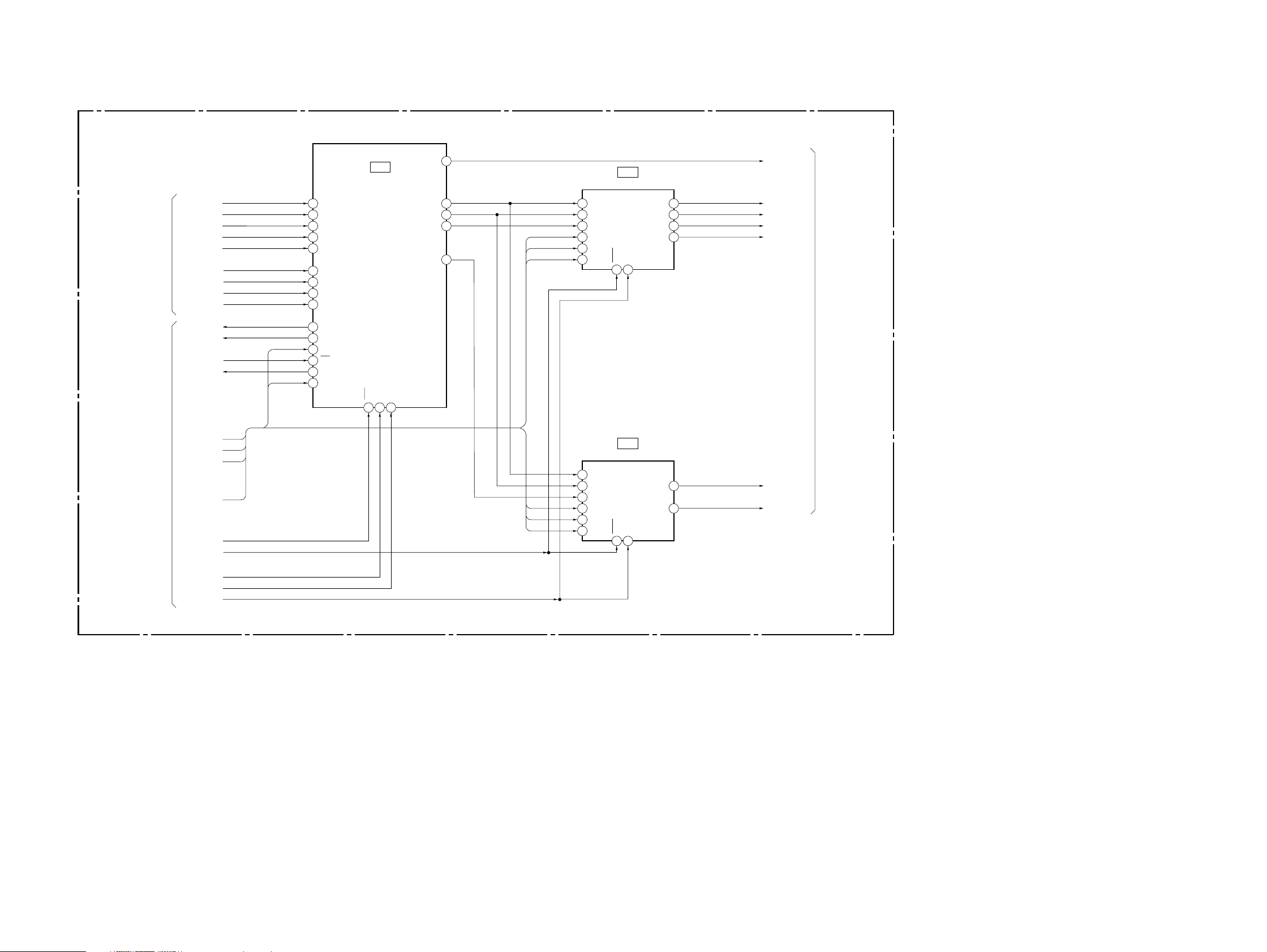
SW-332 (CHUCK SENSOR) PRINTED WIRING BOARD AND SCHEMATIC DIAGRAM
S101
S102
S103
JL101
JL102
JL103
JL104
1SS355TE-17
D101
CL105
2P
CN102
1GND
2S101
CN101
4P
GND 1
CKSW1 2
CKSW2 3
OCSW1 4
1
A
B
C
43
05
SW-332 BOARD
25
MB-85 BOARD
CN009
(SEE PAGE 4-32)
CN604
FL-111 BOARD
(SEE PAGE 4-49)
S101-103
(CHUCK SENSOR)
– Ref. No.: SW-332 board; 2,000 series –
There are few cases that the part isn't mounted in this model is printed on this diagram.
DVP-F11
FR-166
(IR/FUNCTION SWITCH)
MB-85
(SIGNAL PROCESS/SERVO)
TK-55
(RF/SERVO)
AU-222
(AUDIO)
FL-111
(IF CON)
HP-122
(HEAD PHONE)
DC-DC Converter Unit
(SWITCHING REGULATOR)
SW-332
(CHUCK SENSOR)
CHUCK SENSOR
4-13 4-14
SW-332
Page 40
DVP-F11
C
E
B
E
B
C
K
KK
AA
A
KK
A
K
A
C
EB
A
MB-85 (SIGNAL PROCESS/SERVO) PRINTED WIRING BOARD
– Ref. No.: MB-85 board; 1,000 series –
MB-85 BOARD (SIDE A)
CN001 D-2
CN002 D-4
CN003 D-5
CN005 B-1
CN006 C-7
CN007 C-1
CN009 A-2
CN010 B-6
CN011 D-6
CN012 D-6
D801 C-6
D802 C-6
D803 C-6
D804 C-6
D805 C-5
D807 C-5
IC001 A-2
IC003 A-3
IC004 B-3
IC202 A-5
IC205 B-6
IC206 B-6
IC302 D-3
IC303 C-4
IC401 C-2
IC501 A-2
IC601 A-4
IC701 C-5
IC904 A-1
Q801 C-5
Q802 C-6
Q803 C-6
There are few cases that the part isn't mounted in this model is printed on this diagram.
MB-85
(SIGNAL PROCESS/SERVO)
TK-55
(RF/SERVO)
FR-166
(IR/FUNCTION SWITCH)
SW-332
(CHUCK SENSOR)
FL-111
(IF CON)
HP-122
(HEAD PHONE)
DC-DC Converter Unit
(SWITCHING REGULATOR)
SIGNAL PROCESS/SERVO
MB-85
AU-222
(AUDIO)
4-15 4-16
Page 41
MB-85 BOARD (SIDE B)
15
2
34
D701 C-2
D806 C-2
IC005 A-6
IC201 A-3
IC203 A-3
IC204 B-2
IC207 A-2
IC304 C-3
IC402 C-5
IC403 C-5
IC404 D-5
IC702 B-1
IC801 C-2
IC802 C-1
IC803 C-1
IC902 A-6
IC907 C-6
DVP-F11
4-17 4-18
SIGNAL PROCESS/SERVO
MB-85
Page 42

DVP-F11
MB-85 (AV DECODER) SCHEMATIC DIAGRAM • See page 4-15 for printed wiring board.
– Ref. No.: MB-85 board; 1,000 series –
1
5432
MB-85 BOARD(1/10)
A
B
MB-85 BOARD(6/10)
MB-85 BOARD(6/10)
MB-85 BOARD(7/10)
MB-85 BOARD(6/10)
C
MB-85 BOARD
(6/10)
D
E
256FS30
MB-85 BOARD
F
(8/10)
ACH12
ACH34
(5/10)
(8/10)
(5/10)
(5/10)
33M30
SDCK
SDEF
XSHD
XSAK
XSRQ
ACH56
LRCK
BCK
CDDOUT
CDDATA
CDBCK
CDLRCK
SD0
SD1
SD2
SD3
SD4
SD5
SD6
SD7
MB-85 BOARD
(8/10)
G
MB-85 BOARD
H
MB-85 BOARD
MB-85 BOARD
I
MB-85 BOARD
J
MB-85 BOARD
(10/10)
K
V3.3V
+3.3V
L
VIDEOY
GND
(9/10)
MB-85 BOARD
(10/10)
MB-85 BOARD
(8/10)
VYC
VIDEOC
GND
VV
VIDEOV
+5V
GND
MB-85 BOARD
M
N
XCS2
XCS3
XRD
XWRH
XAVDIT
XAVDWT
DACK0
DREQ0
DACK1
DREQ1
HD0
HD1
HD2
HD3
HD4
HD5
HD6
HD7
HD8
HD9
HD10
HD11
HD12
HD13
HD14
HD15
05
HD0
HD1
HD2
HD3
HD4
HD5
HD6
HD7
HD8
HD9
HD10
HD11
HD12
HD13
HD14
HD15
CL403
CL404
CL405
CL406
CL407
CL408
CL409
SD0
SD1
SD2
SD3
SD4
SD5
SD6
SD7
B+
B+
B+
FL404
FL401
C401
10u
10V
FL405
C414
10u
10V
HD11
HD10
HD9
HD8
HD7
HD6
HD5
HD4
HD3
HD2
HD1
HD0
C416
0.01u
B
R411
10k
C418
0.01u
SD0
B
SD1
SD2
SD3
SD4
SD5
SD6
SD7
C402
100u
4V
CL410
CL411
CL412
CL413
CL414
CL415
B+
3.3
4.9
45
123
CL416
CL417
1.3
C415
0.01u
4.9
B
CL476
CL401
B+
B+
R426
IC404
NJM2370U33-TE2
IC404
+3.3V REG
R410
CL475
B+
1k
B+
1
GND
1.1
2
HD11/PD3
1.1
3
HD10/PD2
0.9
4
HD9/PD1
1.5
5
HD8/PD0
3.3
6
VDD
1.5
7
HD7
1.9
8
HD6
1.3
9
HD5
1.6
10
HD4
11
GND
1.3
12
HD3
0.8
13
HD2
0.8
14
HD1
1.1
15
HD0
3.3
16
VDD
17
N.C.
18
GND
1.1
19
ACLKI
20
GND
1.3
21
ACH120
0.1
22
ACH340
0.1
23
ACH560
3.3
24
VDD
1.6
25
LRCKO
1.6
26
BCKO
1.6
27
DO
28
GND
1.6
29
CDIN2I
0
30
CDIN1I
1.6
31
CDBCKI
1.6
32
CDLRKI
0
33
CDEMPI
34
N.C.
35
GND
1.5
36
CRPCLKI
3.3
37
VDD
0.9~2.2
38
DT0I
0.9~2.2
39
DT1I
0.9~2.2
40
DT2I
0.9~2.2
41
DT3I
0.9~2.2
42
DT4I
0.9~2.2
43
DT5I
44
GND
0.9~2.2
45
DT6I
0.9~2.2
46
DT7I
1.6
47
ICLKI
3.3
48
IERRIN
3.3
49
ISTARTIN
0
50
IVALIN
2.8
51
IREQON
52
PWMO
B+
B+
R428
R427
220
220
220
C432
0.01u
B
HD12
HD13
HD14
HD15
197
198
199
200
201
202
203
204
205
206
207
208
1.1
3.3
53
R429
220
3.3
1.5
1.2
0.9
HD12/PD4
VDD
0.6
3.3
3.3
3.3
3.3
3.3
VDD
GND
HD15/PD7
HD14/PD6
HD13/PD5
R/B-Y OUT54AGND55AVDD56B/R-Y OUT57G/Y OUT58AGND59AVDD60Y_OUT61C_OUT62AGND63AVDD64COMP_OUT65VGO66VBD67AGND68AVDD69VREFI70IREFI71FLDO72HSYNCON73GND74PDI775PDI676PDI577PDI478VDD79PDI380PDI281PDI182PDI083VDD84GND85PDO086PDO187PDO288PDO389GND90PDO491PDO592PDO693PDO794VDD95GND96N.C.97NR_SDOUT98NR_SENO99FLDI
3.3
1.7
0.6
C420
0.01u
B
R430
R431
220
220
DMRQ0ON
3.3
DMACK0IN
0.6
DMRQION
1
1.7
DMACK1IN
HWAITON
2
3.3
C422
0.01u
B
MB-85 BOARD(2/10)
(SEE PAGE 4-21)
MB-85 BOARD(6/10)
1817161514
1
131211109876
XIFAVRST
1
2
3
4
5
6
7
8
9
10
11
12
13
15
16
17
18
HA3
HA2
HA1
HA0
R403
10k
191
192
193
194
195
196
3.3
GND
HIRQON
3.3
3.3
HCPUMDI
HRW/HWIN
HCS/HRDIN
HAD0I
2.001.6
HAD1I
HA4
186
187
188
189
190
1.5
2.4
3.3
1.8
1.5
VDD
HAD4I
HAD3I
HAD2I
3
0.6
2.1
1.1
3.3
0.4
0.4
1.6
3.0
1.8
B
C443
0.01u
3300
R405
1k
RV401
C403
C404
0.1u
0.1u
R404
B
B
RV401
VIDEO
LEVEL
ADJ
PDI7
0
1200
R406
HAD5I
HA5
185
0.8
1.1
HAD6I
PDI6
HA6
184
1.2
0.8
HAD7I
IC401
AV DECODER
1.1
1.6
PDI5
HA8
HA7
182
183
1.4
HAD8I
IC401
CXD1930BQ
3.3
PDI4
HAD9I
HA9
HA11
HA10
HA12
177
178
179
180
181
3.3
1.3
1.6
3.3
GND
HAD12I
HAD11I
HAD10I
1.0
0.4
1.1
0.9
3.3
C425
PDI3
PDI2
PDI1
PDI0
HAD13I
0.01u
RB402
HA17
HA16
HA15
HA14
HA13
172
173
174
175
176
0.6
1.6
3.3
3.3
0.6
HAD17I
HAD16I
HAD15I
HAD14I
0.9
1.1
0.4
1.0
B
10k
PDO0
PDO1
PDO2
PDO3
HAD18I
HA21
HA20
HA19
HA18
C434
0.01u
B
166
167
168
169
170
171
3.3
3.3
3.302.8
0.8
VDD
HAD22I
HAD21I
HAD20I
HAD19I
1.6
1.1
1.1
1.8
3.3
C426
0.01u
PDO4
PDO5
PDO6
PDO7
B
L402
10uH
R407
HAD23I
C436
0.01u
B
C441
100u
10k
165
3.3
TESTIN
4V
157
158
159
160
161
162
163
164
1.6
GND
0
SCLKIN
3.3
1.6
3.3
3.3
VDD
VDD
3.3
100
CL418
GND
CLKI
AVDD
AGND
HSYNCIN
SHTDWNIN
RSTIN
VDD
3.3
3.3
3.3
101
102
103
104
R409
0
CL419
C438
0.01u
B
B+
1.9
SDDQ0
156
2.2
SDDQ15
155
GND
154
2.0
SDDQ1
153
2.0
SDDQ14
152
3.3
VDD
151
1.5
SDDQ2
150
2.1
SDDQ13
149
GND
148
2.0
SDDQ3
147
2.1
SDDQ12
146
3.3
VDD
145
2.1
SDDQ4
144
2.0
SDDQ11
143
GND
142
2.1
SDDQ5
141
1.5
SDDQ10
140
3.3
VDD
139
2.0
SDDQ6
138
2.1
SDDQ9
137
GND
136
2.2
SDDQ7
135
1.9
SDDQ8
134
3.3
VDD
133
0.1
SDDQM0O
132
0.1
SDDQM1O
131
3.0
SDWEON
130
2.7
SDCASON
129
GND
128
SDCLKO
127
GND
126
1.6
DCLKI
125
3.3
VDD
124
2.5
SDRASON
123
3.2
SDCKEO
122
2.7
SDCS0ON
121
3.0
SDCS1ON
120
GND
119
1.4
SDAD11O
118
0.1
SDAD9O
117
0.1
SDAD10O
116
0.1
SDAD8O
115
3.3
VDD
114
0.1
SDAD0O
113
1.7
SDAD7O
112
0.6
SDAD1O
111
2.2
SDAD6O
110
GND
109
1.2
SDAD2O
108
1.7
SDAD5O
107
1.4
SDAD3O
106
1.5
SDAD4O
105
NO MARK:DVD/CD PLAY
SIGNAL PATH
VIDEO SIGNAL
CL420
CL421
CL422
CL423
C433
0.01u
B
CL424
CL425
CL426
CL427
C431
0.01u
B
CL428
CL429
CL430
CL431
CL432
CL433
CL434
CL435
CL436
CL437
CL438
CL439
CL440
C428
0.01u
B
CL441
CL442
CL443
CL444
CL445
CL446
CL447
CL448
CL449
CL450
CL451
CL452
CL453
CL454
CL455
CL456
YCHROMA Y/CHROMA
DDT15
DDT14
DDT13
DDT12
DDT11
DDT10
DDT0
DDT1
DDT2
DDT3
DDT4
DDT5
DDT6
DDT9
DDT7
DDT8
AUDIO
SIGNAL
DAD11
DAD9
DAD10
DAD8
DAD0
DAD7
DAD1
DAD6
DAD2
DAD5
DAD3
DAD4
PB
AV DECODER
MB-85 (1/10)
4-19 4-20
Page 43

MB-85 (SDRAM) SCHEMATIC DIAGRAM • See page 4-15 for printed wiring board.
– Ref. No.: MB-85 board; 1,000 series –
1
5432
MB-85 BOARD(2/10)
A
B
C
D
E
1
MB-85 BOARD(1/10)
(SEE PAGE 4-20)
F
G
H
I
J
K
L
1
2
IC402
3
4
C405
0.01u
B
C406
0.01u
C410
0.01u
C411
0.01u
CL477
B
CL478
B
B
DDT0
DDT1
DDT2
DDT3
DDT4
DDT5
DDT6
DDT7
DAD11
DAD10
DAD0
DAD1
DAD2
DAD3
5
6
7
8
DAD11
DAD10
DAD0
DAD1
DAD2
DAD3
DDT0
DDT1
DDT2
DDT3
DDT4
DDT5
DDT6
DDT7
9
10
11
12
13
15
16
17
18
05
16M SDRAM
KM416S1020CT-G10TIC402
16M SDRAM
DQ15
DQ14
VSSQ
DQ13
DQ12
VCCQ
DQ11
DQ10
VSSQ
VCCQ
DQMU
DQ15
DQ14
VSSQ
DQ13
DQ12
VCCQ
DQ11
DQ10
VSSQ
VCCQ
DQMU
VSS
50
2.2
49
2.0
48
47
2.1
46
2.1
45
3.3
44
2.0
43
1.5
42
41
2.1
DQ9
40
1.9
DQ8
39
3.3
38
N.C.
37
0.1
36
1.6
CLK
35
3.2
CKE
34
N.C.
33
0.1
A9
32
0.1
A8
31
1.7
A7
30
2.2
A6
29
1.7
A5
28
1.5
A4
27
VSS
26
C408
0.01u
B+
VSS
50
2.2
49
2.0
48
47
2.1
46
2.1
45
3.3
44
2.0
43
1.5
42
41
2.1
DQ9
40
1.9
DQ8
39
3.3
38
N.C.
37
0.1
36
1.6
CLK
35
3.2
CKE
34
N.C.
33
0.1
A9
32
0.1
A8
31
1.7
A7
30
2.2
A6
29
1.7
A5
28
1.5
A4
27
VSS
26
C413
0.01u
3.3
1
VCC
1.9
2
DQ0
2.0
3
DQ1
4
VSSQ
1.5
5
DQ2
2.0
6
DQ3
3.3
7
VCCQ
2.1
8
DQ4
2.1
9
DQ5
10
VSSQ
2.0
11
DQ6
2.2
12
DQ7
3.3
13
VCCQ
0.1
14
DQML
3.0
15
WE
2.7
16
CAS
2.5
17
RAS
2.7
18
CS
1.4
19
A11(BA)
0.1
20
A10/AP
0.1
21
A0
0.6
22
A1
1.2
23
A2
1.4
24
A3
3.3
25
VCC
IC403
KM416S1020CT-G10TIC403
3.3
1
VCC
1.9
2
DQ0
2.0
3
DQ1
4
VSSQ
1.5
5
DQ2
2.0
6
DQ3
3.3
7
VCCQ
2.1
8
DQ4
2.1
9
DQ5
10
VSSQ
2.0
11
DQ6
2.2
12
DQ7
3.3
13
VCCQ
0.1
14
DQML
3.0
15
WE
2.7
16
CAS
2.5
17
RAS
3.0
18
CS
1.4
19
A11(BA)
0.1
20
A10/AP
0.1
21
A0
0.6
22
A1
1.2
23
A2
1.4
24
A3
3.3
25
VCC
DVP-F11
11109876
• Waveforms
1 IC401 ya
27M30
MB-85 BOARD(8/10)
FL402
B+
HA21
HA20
HA19
HA18
HA17
HA16
HA15
HA14
HA13
HA12
HA11
HA10
HA9
HA8
HA7
HA6
HA5
HA4
HA3
HA2
HA1
HA0
CL457
CL458
CL459
CL460
CL461
CL462
CL463
CL464
CL465
CL466
CL467
CL468
CL469
CL470
CL471
CL472
CL473
CL474
NO MARK:DVD PLAY
CD:CD PLAY
HA21
HA20
HA19
HA18
HA17
HA16
HA15
HA14
HA13
HA12
HA11
MB-85 BOARD
HA10
HA9
HA8
HA7
HA6
HA5
HA4
HA3
HA2
HA1
HA0
B+
(6/10)
GND
MB-85 BOARD(10/10)
+3.3V
2 IC401 ys
3 IC401 yg
1.1 Vp-p (H)
816 mVp-p (H)
1.2 Vp-p (H)
DAD9
DAD8
DAD7
DAD6
DAD5
DAD4
C440
10V
DAD9
DAD8
DAD7
DAD6
DAD5
DAD4
C439
10u
10V
B+
FL403
10u
PDO0
PDO1
PDO2
PDO3
PDO4
PDO5
PDO6
PDO7
PDI0
PDI1
PDI2
PDI3
PDI4
PDI5
PDI6
PDI7
DDT15
DDT14
DDT13
DDT12
B
DDT11
DDT10
DDT9
DDT8
DDT15
DDT14
DDT13
DDT12
B
DDT11
DDT10
DDT9
DDT8
SDRAM
4-224-21
MB-85 (2/10)
Page 44
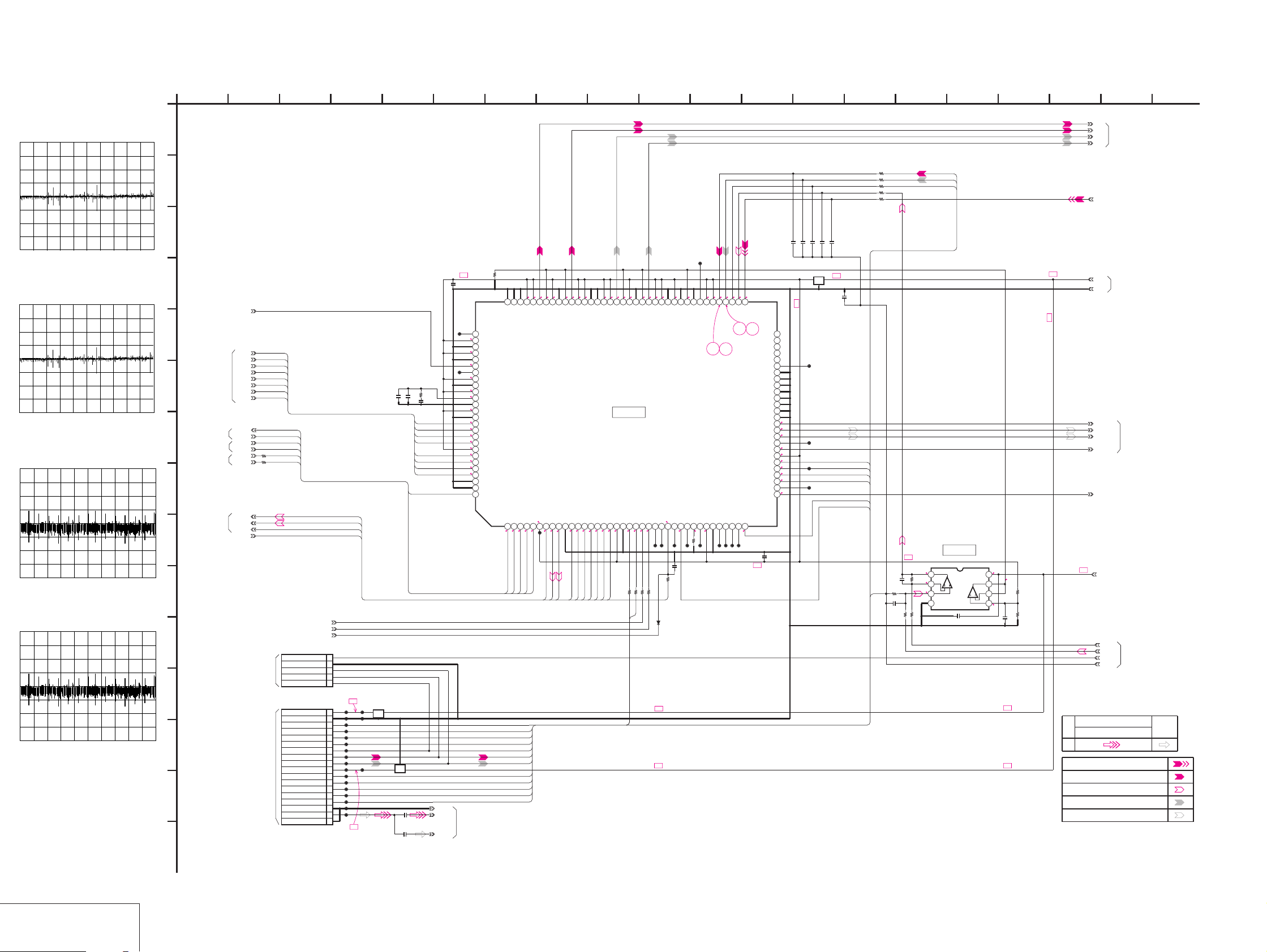
DVP-F11
MB-85 (SERVO DSP) SCHEMATIC DIAGRAM • See page 4-15 for printed wiring board.
– Ref. No.: MB-85 board; 1,000 series –
• Wavef orms
1 IC701 yl (DVD play)
500 mV/DIV 50 ms/DIV
1.4 Vp-p
2 IC701 yl (CD play)
500 mV/DIV 200 mV/DIV
1.7 Vp-p
3 IC701 yk (DVD play)
100 mV/DIV 5 ms/DIV
180 mVp-p
4 IC701 yk (CD play)
500 mV/DIV 50 ms/DIV
860 mVp-p
1
MB-85 BOARD(3/10)
A
B
C
D
MB-85 BOARD(8/10)
E
MB-85 BOARD(6/10)
F
MB-85 BOARD(7/10)
G
MB-85 BOARD(6/10)
MB-85 BOARD(7/10)
H
MB-85 BOARD(4/10)
MB-85 BOARD(7/10)
I
J
K
L
M
N
O
N27MSDP
HD10
HD11
HD12
HD13
HD14
HD15
XSDPIT
XSDPCS
XSDPWR
XSDPRD
SLDA
SLDB
STVC
XSDPRST
TK-55 BOARD
CN003
(SEE PAGE 4-12)
28
HD8
HD9
HA1
HA0
R757
R758
0
TO RF JIG
(CHECK)
3 16151210
HD8
HD9
HD10
HD11
HD12
HD13
HD14
HD15
XSDPIT
XSDPCS
HA1
HA0
0
XSDPWR0
XSDPRD0
MB-85 BOARD(5/10)
MB-85 BOARD(4/10)
MB-85 BOARD(6/10)
05
LOCK
INLIM
X3VRST
5PCN012
18PCN002
4
SLDA
SLDB
STVC
XSDPRST
1RF
2GND
3FE
4TE
5PI
B+
CL070
CL009
185V
CL072
CL025
17GND
CL010
16MIRR
CL012
15SSDFCTI
CL021
14TZC
CL013
132VC
CL011
12PI
CL014
11TE
CL015
10FE
CL078
CL016
93.3V
CL017
8SSCK
CL018
7SSWD
CL001
6SSRD
CL019
5SSCS
CL020
4SSDFCT
CL023
3RF-
CL024
2RF+
1GND
B+
5
C708
R722
0.1u
22
B
C709
0.22u
B
HD15
HD14
HD13
HD12
HD11
HD10
HD9
HD8
XSDPIT
FL001
FL005
C001
0.01u
C002
0.0047u B
6
C702
0.01u
B+
B
CL762
3.3
3.3
1.7
CL763
3.3
3.3
GND
DVDRF
CDRF
1.2
3.3
1.5
1.2
0.9
1.1
3.3
1.2
1.1
0.9
1.5
RF
MB-85 BOARD(5/10)
C707
0.01u
B
B
7
R701
47
3.3
3.3
97
98
99
100
101
102
VRT0
DAB0
VCCA5
GNDA5
TESTSIB1
TESTSIB0
TESTSOB
103
PLLMD
104
TESTB(VSS)
105
VDD
106
VSS
107
X2/CLKIN
108
X1
109
VDD
110
VSS
111
VCCA6
112
LF
113
GNDA6
114
VDD
115
VSS
116
HD7/HIO
117
HD6/HO6
118
HD5/HO5
119
HD4/HO4
120
VDD
121
HD3/HO3
122
HD2/HO2
123
HD1/HO1
124
HD0/HO0
125
VSS
126
SRPRN
127
HINT/HTXD
128
HRD/HRXD2HWR/HFS3HCS4EA15EA0/HCK6VDD7PWM28PWM19PWM010VSS11EMU112EMU013TDO14TCK15TDI16TMS17TRST18VDD19VSS20TRREF21TRIN22FGREF23FGIN24PGREF25PGIN26RS27LG28DFCTI29HEAD30CLKODIS31CLKOUT132VDD
3.3
1
0
2.0
3.3
1.9
3.1
CL781
HA0
HA1
XSDPWR0
XSDPRD0
XSDPCS
MIRR
SSDFCTI
TZC
2VC
PI
TE
FE
SSCK
SSWD
SSRD
SSCS
SSDFCT
2.0
0.8
3.3
0.8
2.0
91
92
94
95
96
DAB193VRB1
VRB0
VSS3V3
VDD3V3
3.3
3.2
1.6
1.6
1.6
STVC
SLDA
SLDB
EMU0
EMU1
9
3.3
0.8
3.3
2.0
3.3
3.3
90
VRT1
VCCA4
1.6
1.7
TCK
TDO
83
84
86
87
88
VRT2
VRB285DAB2
VCCA3
GNDA389GNDA4
VDD3V2
IC701
CXD8791AQ
IC701
SERVO DSP
3.3
0.1
0.3
3.2
3.2
TRST
TMS
TDI
3.3
82
VSS3V2
3.3
0.2
1k
R7201kR7211kR7511kR752
TZC
MIRR
3.3
3.3
2.1
0.8
76
77
78
79
80
VRT3
DAB381VRB3
VCCA2
GNDA2
VDD3V1
3.3
2.2
CL769
CL715
CL780
R755
10k
XSDPRST
D701
1SS355TE-17
B+
B+
11
CL771
0.8
3.3
73
74
75
VRBA
GNDA1
VSS3V1
1.8
2.5
2.0
3.3
3.3
68
69
71
72
ADC1
ADC070VRTA
TESTA
VCCA1
3
1
2
GIO15
VSS
GIO14
GIO13
33
34
35
36
0
10k
0.1
R748
CL770
CL772
C717
0.01u
B
37
3.3
CL773
CL774
CL775
CL776
1.8
65
GIO1238GIO11
0
3.1/
CD2.4
ADC466ADC367ADC2
4
TESTSOA
TESTSIA0(VSS)
TESTSIA1(VSS)
TEST0(VSS)
TEST1(VSS)
TEST2(VSS)
TEST3(VSS)
TESTC(VSS)
GIO0/INT2
GIO1/INT3
GIO2/INT4
GIO3/INT5
GIO4/TMC0
GIO5/TMC1
GIO6/TMC2
B+
20191817
B
B
C713
C714
C715
4700p
4700p
4700p
B+
13 14
B
B
B
0.1u
C711
C712
4700p
FL701
B+
C710
0.01u
B
TRD+
TRD-
MB-85 BOARD(4/10)
FCD+
FCD-
R702
470
470
R703
470
R704
470
R705
1k
R706
TE
FE
PI
MB-85 BOARD(4/10)
SPFG
B+
+3.3V
MB-85 BOARD(10/10)
GND
B+
ADC5
64
ADC6
63
ADC7
62
ADC8
61
ADC9
60
59
58
57
56
55
54
53
52
VSS
51
50
49
48
47
46
VDD
45
44
43
GIO7
42
GIO8
41
GIO9
40
GIO10
39
C701
0.01u
B
CL777
3.3
3.2
1.7
CL778
3.2
3.3
0
0.3
CL704
3.3
3.3
CL779
3.3
SSDFCT
SSDFCTI
SSCS
SSRD
SSWD
SSCK
IC702
NJM2904V(TE2)
SLED ERR AMP/POWER SUPPLY
1.8
1234
R710
2.2
82k
2.1
82k
R708
IC702
4.9
0.8
R712
33k
5678
0.8
R711
C703
0.1u
B
10k
0.1u
B
B+
C706
0.047u
B
R709
82k
2VC
C705
0.047u
B
82k
R707
B+
FGMODE
TLTA
TLTB
TILTMUTE
FCSON
B+
+5V
NO MARK:DVD PLAY
CD:CD PLAY
SIGNAL PATH
VIDEO SIGNAL
Y/CHROMA
2.5VC
SLDER
RFMON
2VC
MB-85 BOARD(4/10)
MB-85 BOARD(7/10)
MB-85 BOARD(10/10)
MB-85 BOARD(4/10)
AUDIO
SIGNAL
PB
B+
SPINDLE SERVO(SPEED AND PHASE)
TRACKING SERVO DVD/CD CDV
SLED SERVO DVD/CD
FOCUS SERVO
SKEW SERVO DVD/CD
SERVO DSP
MB-85 (3/10)
4-23 4-24
Page 45

MB-85 (DRIVE) SCHEMATIC DIAGRAM • See page 4-15 for printed wiring board.
– Ref. No.: MB-85 board; 1,000 series –
1
2345 67891011121314151617
DVP-F11
18 19
MB-85 BOARD(4/10)
A
MB-85 BOARD(7/10)
MB-85 BOARD(3/10)
B
C
MB-85 BOARD(5/10)
D
E
MB-85 BOARD(7/10)
F
MB-85 BOARD(3/10)
G
MB-85 BOARD(7/10)
H
MB-85 BOARD(3/10)
I
J
MB-85 BOARD(5/10,6/10)
K
MB-85 BOARD(3/10)
L
M
N
TK-55 BOARD
CN004
(SEE PAGE 4-12)
SPDLSTOP
FGMODE
SPGAIN
LDMP/DMP
LDMM/DMM
2.5VC
INLIM
RFMON
MDP0
SLDA
SLDB
STVC
SPFG
MDS0
R865
10k
R866
10k
R819
220k
R823
10k
R821
39k
R824
10k
R826
5600
C816
10V
1.6
R828
22k
0
1.7
Q802
2SD1819A-QRS-TX
Q802,803
GAIN CONTROL
SLDA
SLDB
STVC
C823
0.01u
R870
330
B+
+5V
GND
2VC
18PCN003
05
CL026
18GND
CL027
17RF MON
16GND
CL030
15TRK-
CL031
14TRK+
CL032
13FCS-
CL033
12FCS+
CL034
11INLIM
CL035
10SLB-
CL036
9SLA+
CL037
8SLB+
CL038
7SLA-
CL039
6SPM+
CL040
5SPM-
CL041
4TIB-
CL042
3TIB+
CL043
2TIA-
CL044
1TIA+
TRK-
TRK+
3.3
R864
FCS-
FCS+
R861
0
SLB-
SLA+
SLB+
SLA-
SPM+
SPM-
TIB-
TIB+
TIA-
TIA+
B
10u
R829
22k
0
2SD1819A-QRS-TX
C824
0.01u
R820
330k
C813
3300p
B
R822
100k
R825
5600
B
C814
0.047u
C815
22u
6.3V
R827
330k
C817
0.22u
B
3.3
1.6
Q803
C830
R871
B
470
0.1u
B
R851
R852
10k
10k
R856
R855
18k
12k
R814
330k
0.5%
R813
150k
0.5%
R815
18k
C819
0.1u
R840
180k
C831
0.1u
B
R853
R854
10k
10k
R818
R816
390k
100k
R817
390k
R846
47k
9.6
1.8
1.8
IN4+
PRE VCC
2.0
2.0
2.5
IN1+
BIAS IN
1 2 3 4 5 6 7 8 9 1011121314
B
R836
150k
STVC
SLDA
REF,VOLT GEN/SPINDLE FG AMP
1.6
1234567
1.6
4.9
V+ V-
2.5
2.5
B+
C832
0.1u
B
C812
3300p
B
2.1
IN4-
OUT4
OUT1
IN1-
C820
220p
R838
180k
R834
150k
IC803
BA10324AFV-E2
IC803
B+
R811
330k
0.5%
C811
0.047u
B
0.5%
R812
150k
2.3
2.3
2.3
IN3-
IN3+
OUT3
IC802
SLED MOTOR
SPINDLE MOTOR
LOADING MOTOR
2.5
2.0
2.5
OUT2
IN2-
IN2+
C821
220p
R839
180k
R835
150k
SLDB
C835
0.1u
B
R872
330
+5V
MB-85 BOARD
(10/10)
GND
30
GND
IC802
BA5983FP-E2
DRIVE
GND
29
3.0/
CD2.4
3.3/CD3.1
3.3/CD3.1
1.9
1.9
8 9 10 11 12 13 14
C825
0.01u
B
B+
D802
1SS355TE-17
D801
DAP202UT106
GND
GND
C833
0.033u
B
C834
0.033u
B
R847
C802
0.1u
2.3
STBY2
2.3
R859
0
B
C822
47u
16V
9.6
VCC2
9.6
VCC1
STBY1
D803
DAP202UT106
56k
0.5%
R831
10k
B+
LDM-
LDM+
R867
B+
D804
DAN202UT106
10k
R868
10k
C818
0.1u
B
R841
68k
R837
82k
R869
10k
B+
SPM-
SPM+
B+
15
16171819202122232425262728
5.6
5.6
VO3-
VO4-
VO3+
VO4+
9.0/CD6.3
4.0/CD4.9
5.9
5.9
5.9
5.9
SLB-
VO1+
VO1-
VO2+
VO2-
SLA-
SLB+
SLA+
R832
10k
TLTB
R843
82k
R845
68k
C837
0.22u
2.1
9.6
PPRE VCC
BIAS
1 2 3 4 5 6 7 8 9 10 11 12 13 14
2.5
2.2
C805
47p
R803
47k
R801
47k
B
IN4-
2.5
2.1
IN4+
IN1+
FCD+
IN3+
OUT4
2.2
IN1-
OUT1
IN2+
2.4
2.1
2.4
C807
100p
C806
R809
47p
82k
R804
47k
B
C809
0.068u
R802
47k
R807
15k
R805
39k
TRD+
FCD-
B+
R857
150k
0.5%
R858
150k
0.5%
R860
56k
0.5%
SPM-
SPM+
B+
TLTA
R842
82k
R844
68k
IN3-
2.1
1.2
OUT3
FOCUS/TRACKING COIL
2.4
IN2-
C808
100p
R810
82k
C810
R808
15k
R806
39k
TRD-
UN5111-TX
INVERTER
C836
0.22u
B
30
IC801
BA5981FP-E2
IC801
TILT MOTOR
DRIVE
OUT2
29
B
0.068u
3.3
Q801
1SS355TE-17
B+
B+
C803
0.1u
B
C801
47u
16V
9.6
2.9
GND
GND
MUTE2
0.1
MUTE1
GND
R873
9.6
GND
D806
1SS355TE-17
3.3
-2.7
1k
D807
TIA-
TIA+
5.7
5.7
DO3-
DO3+
PVCC
6.0
PVCC
DO2+
DO2-
6.2
TRK-
+TRK
DAN202UT106
NO MARK:DVD PLAY
SIGNAL PATH
TIB-
TIB+
5.7
5.7
15
16171819202122232425262728
DO4-
DO1-
6.3
5.8
FCS-
+FCS
D805
CD:CD PLAY
B+
DO4+
DO1+
TLTA
TLTB
TRD+
TRD-
FCD+
FCD-
LDM-
LDM+
R006
R005
R004
B+
CL095
1k
CL084
1k
CL154
CL153
1k
CL082
CL152
10k
10k
10kR001
R003
R002
CN011
1 LDM-
2 LDM+
3 CKSW1
4 OCSW1
5 GND
6 OCSW2
B+
+3.3V
MB-85 BOARD(5/10,6/10)
B+
S10V
MB-85 BOARD(10/10)
TLTA
MB-85 BOARD(3/10)
TLTB
SLDER
TRD+
MB-85 BOARD(3/10)
TRD-
FCD+
FCD-
TILTMUTE
MB-85 BOARD(3/10)
MB-85 BOARD(7/10)
XDRVMUTE
MB-85 BOARD(6/10)
X3VRST
OCSW1
CKSW1
MB-85 BOARD(7/10)
CKSW1A
OCSW1A
6P
TK-55 BOARD
CN005
(SEE PAGE 4-12)
OCSW2
MB-85 BOARD(7/10)
SPINDLE SERVO(SPEED AND PHASE)
TRACKING SERVO DVD/CD CDV
SLED SERVO DVD/CD
FOCUS SERVO
SKEW SERVO DVD/CD
4-25 4-26
DRIVE
MB-85 (4/10)
Page 46

DVP-F11
MB-85 (ARP) SCHEMATIC DIAGRAM • See page 4-15 for printed wiring board.
– Ref. No.: MB-85 board; 1,000 series –
1
MB-85 BOARD(5/10)
A
MB-85 BOARD
(4/10)
+5V
+3.3V
GND
B
C
D
E
F
DVDRF
MB-85 BOARD
(3/10)
G
CDRF
GNDRF
H
I
J
K
MB-85 BOARD
(4/10)
MB-85 BOARD
(7/10)
L
MB-85 BOARD
(3/10)
MB-85 BOARD
(7/10)
M
05
MDS0
MDP0
DFCT
NORF
LOCK
FWON
LOCK
XARPWR
XARPRD
XARPCS
B+
FL301
C321
100u
6.3V
CL340
123
4.9
1.3
C307
10u
C339
10V
0.01u
C319
B
B+
10u
10V
C320
0.01u
B
4.9
3.3
45
B+
FL302
IC302
NJM2370U33-TE2
IC302
+3.3v REG
MD15
MD14
MD13
MD11
MD10
MD09
MD12
C324
0.01u
B
MD08
B+ B+
3.0
3.0
3.0
3.0
169
170
171
172
173
174
175
1
2
3
4
5
6
7
8
9
10
11
12
13
14
15
16
17
18
19
20
21
22
23
24
25
26
27
28
29
30
31
32
33
34
35
36
37
38
39
40
41
42
43
44
EAD3
EAD4
EAD5
EAD6
EAD7
PLDIR
3.3
VDD
PLCKI
PLCKO
VSS
RFD
VDD3V1
VSS3V1
VRB
VRBS
VSSA1
1.6/CD0.5
RFIN1
AIN
RFIN2
0.5/CD1.6
VDDA1
VRTS
VRT
VDD3V1
VSS3V2
VDD3V2
IREF
AOUT
VSSA2
VDDA2
BIAS
VREF
VDDA3
Y
FR1
FR2
FR3
INM
INP
VSSA3
3.3
VDDA4
2.4
R2
1.1
R1
1.8
VCO
VSSA4
176
VSS
EAD0
EAD1
EAD2
MD15
MD14
MD13
MD12
1
2
VDD46VCK47VSS48TESTA49MDS050MDS151MON52MDP053MDP154VDD55DFCT
0
45
10k
3.3
CL305
1.8
1.6
CL306
CL307
R324
R340
10k
R315
10k
B+
C310
0.01u
B
CL301
CL302
CL303
CL342
CL343
R306
220
0.5%
CL344
R305
22k
0.5%
R307
C327
33k
0.01u
0.5%
B
R308
R309
C304
0.068u
B
10kR323
C316
0.01u
B
C337
0.01u
B
10k
R313
10kR314
C312
0.01u
B
C313
0.01u
B
C314
0.01u
B
C315
0.01u
B
R320
1800
0.5%
R316
2200
0.5%
R321
1k
0.5%
2200
27k
2200R310
C318
0.01u
B
C338
R341
100
0.01u
B
10k
0.5%
R322
10k
0.5%
C322
C309
C317
C344
100p
0
CL341
1.5
1.6
3.3
0.7
1.6
3.3
2.8
3.3
3.3
1.0
0.6
3.3
0.01u
2.4
B
0.1u
1.0
B
0.01u
3.3
B
1.8
1.6
1.8
1.6
1.7
R318
220k
R319
6800
B+
3.0
3.0
3.0
3.0
3.3
168
VDD
CL308
163
164
165
166
167
MD08
MD09
MD10
MD11
JITPWM58LOCK59FWON60XWR61XRD62VSS63D064D165D266D367D468D569VDD70D671D772TEST73A074A175A276A377VSS78SCEN79A480A581A682A783XINT84XCS85VDD86XWAT87XRST88TEST0
NORF
1.7/CD0.2
0.4
0/CD0.6
3.3
56
57
10kR325
3.3
CL335
C323
C325
0.01u
0.1u
B
B
851132 10 12 13 14 15 16 17 186
947
FL303
B+
• Wavef orms
1 IC303 qj (DVD play)
500 mV/DIV 100 ns/DIV
B+
MD07
MD06
MD05
MD04
MD03
MD02
MD01
MD00
3.0
3.0
155
156
MD02
IC303
CXD8784R
IC303
ARP2
1.1
1.1
HD9
HD10
MD01
0.2
3.0
3.0
151
152
153
154
XOE
VSS
MD00
3.3
0.9
1.1
1.2
HD11
HD12
HD13
3.0
162
VSS
MD07
0
157
158
159
160
161
VDD
MD03
MD04
MD05
MD06
1.9
3.2
0.9
1.5
HD8
3.0
3.3
3.0
3.0
3.0
XRAS
MA9
MA8
MA7
MA6
MA5
MA4
MA3
MA2
MA1
C328
0.01u
B
3.3
0.1
0.2
0.2
0.2
0.2
3.2
3.3
3.1
149
150
VDD
XCAS
10kR326
1.5
HD14
HD15
0.2
140
141
142
143
144
145
146
147
148
VSS
MA4
MA5
MA6
MA7
MA8
MA9
XMWR
0
10kR327
2.4
1.5
2.0
3.3
HA1
HA0
1.5
1.8
HA2
0.8
HA3
HA4
HA5
MA0
CL309
0.2
0.2
138
139
VDD
MA2
MA3
3.2
0.8
HA6
HA7
CL310
0.2
0.1
133
134
135
136
137
VSS
MA0
MA1
ESTB
MNT7
MNT6
CL311
132
MNT5
CL312
131
MNT4
CL313
130
3.3
VDD
129
MNT3
CL314
128
MNT2
CL315
127
MNT1
CL316
126
MNT0
CL317
125
VSS
124
SCKI
123
VDD
122
3.3
MCKI
121
VSS
120
SQCK
119
0
SQSO
CL318
118
SBSO
CL319
117
EXCK
116
0
SCOR
CL320
115
WFCK
CL321
114
MD2
113
3.3
VDD
112
3.3
MUTE
111
0
DOUT
110
1.6
LRCK
109
1.6
BCLK
108
1.6
DATA
107
0
VSS
106
SD7
105
0.9-2.2
SD6
104
0.9-2.2
SD5
103
0.9-2.2
SD4
102
0.9-2.2
SD3
101
0.9-2.2
SD2
100
0.9-2.2
VDD
99
3.3
SD1
98
0.9-2.2
SD0
97
0.9-2.2
SDEF
96
3.3
XSAK
95
3.0
XSRQ
94
3.0
XSHD
93
3.3
VSS
92
1.6
SDCK
91
0
ETST
90
SCMD
0
3.3
B
10k
3.3
3.2
3.3
C329
0.01u
C331
0.01u
B
R338
10k
R328
R337
100
R330
89
0
R339
10k
C333
0.01u
B
1.5
R331
10k
R332
10k
C334
0.01u
B
R329
10k
10k
CL336
CL337
CL338
CL339
CL322
CL323
CL324
CL325
CL326
CL327
CL328
CL329
CL330
CL331
CL332
CL333
CL334
C341
0.01u
CL345
B
MD00
3.3
MD01
3.0
MD02
3.0
MD03
3.0
3.3
MD04
3.0
3.0
MD05
3.0
MD06
3.0
MD07
3.2
3.0
MA0
MA1
MA2
MA3
0.2
0.1
0.2
0.2
3.3
C343
0.01u
B
SD7
SD6
SD5
SD4
SD3
SD2
SD1
SD0
SDEF
XSRQ
XSAK
XSHD
SDCK
IC304
1
VDD
2
I/O0
3
I/O1
4
I/O2
5
I/O3
6
VDD
7
I/O4
8
I/O5
9
I/O6
10
I/O7
11
N.C.
15
N.C.
16
N.C.
17
WE
18
RAS
19
NC
20
NC
21
A0
22
A1
23
A2
24
A3
25
VDD
IC304
16M DRAM
KM416V1200CT-L6T
SDEF
XSAK
XSRQ
XSHD
SDCK
HA0
HA1
HA2
HA3
HA4
HA5
HA6
HA7
HD8
HD9
HD10
HD11
HD12
HD13
HD14
HD15
I/O15
I/O14
I/O13
I/O12
I/O11
I/O10
LCAS
UCAS
SD7
SD6
SD5
SD4
SD3
SD2
SD1
GND
50
MD15
3.0
49
MD14
3.0
48
MD13
3.0
47
MD12
3.0
46
GND
45
MD11
3.0
44
MD10
3.0
43
MD09
3.0
I/O9
42
MD08
3.0
I/O8
41
N.C.
40
N.C.
36
3.1
35
3.1
34
0.2
OE
33
0.2
A9
A8
A7
A6
A5
A4
GND
MA9
32
0.2
MA8
31
0.2
MA7
30
0.2
MA6
29
0.2
MA5
28
0.1
MA4
27
26
2 IC303 ql (CD play)
500 mV/DIV 200 ns/DIV
1.6 Vp-p
1.6 Vp-p
33MARP
MB-85 BOARD(8/10)
MD2
MUTE
CDDOUT
CDLRCK
CDBCK
CDDATA
SD7
SD6
SD5
SD4
SD3
SD2
SD0
HD10
HD11
HD12
HD13
HD14
HD15
SD1
SD0
SDEF
XSAK
XSRQ
XSHD
SDCK
XARPRST
XARPWT
XARPIT
HA0
HA1
HA2
HA3
HA4
HA5
HA6
HA7
HD8
HD9
MB-85 BOARD
(6/10)
MB-85 BOARD
(6/10)
MB-85 BOARD
(7/10)
MB-85 BOARD
(1/10,8/10)
MB-85 BOARD
(1/10)
MB-85 BOARD
(1/10)
MB-85 BOARD
(7/10)
NO MARK:DVD PLAY
CD:CD PLAY
SIGNAL PATH
VIDEO SIGNAL
Y/CHROMA
PB
SPINDLE SERVO(SPEED AND PHASE)
AUDIO
SIGNAL
ARP
MB-85 (5/10)
4-27 4-28
Page 47

MB-85 (SYSTEM CONTROL) SCHEMATIC DIAGRAM • See page 4-15 for printed wiring board.
– Ref. No.: MB-85 board; 1,000 series –
1
28
3 16151210
4
5 21
6
7
9
DVP-F11
11
13 14
20191817
22
MB-85 BOARD(6/10)
A
B
MB-85 BOARD(8/10)
C
MB-85 BOARD(7/10)
D
TO DIAG JIG
(CHECK)
E
MB-85 BOARD(8/10)
MB-85 BOARD(8/10,9/10)
F
G
H
I
MB-85 BOARD(10/10)
J
MB-85 BOARD(9/10)
K
L
FL-111 BOARD
CN602
(SEE PAGE 4-49)
CN006
M
MB-85 BOARD(7/10)
MB-85 BOARD(1/10)
N
05
B+
IC204
IDT71V016S20PHAU-TL
IC204
1M SRAM
XRAMWE
XUB
XLB
MB-85 BOARD(7/10)
B+
B+
MB-85 BOARD(4/10)
B+
B+
+3.3V
GND
B+
CL201
CKSEL
XEWC
XEBSY
XECS
CN010
6P
15P
AMUTE
VMUTE
XIFAVRST
CL130
1TXD
CL131
2RXD
CL132
3DIAG_ON
CL123
4GND
CL003
5N.C.
CL133
6+5V
CL102
SI1
SO1
B+
+3.3V
FB043
CL136
15+3.3V
CL137
14MICCONT
13GND
CL138
12A1OUT
CL139
11A1IN
CL140
10SLINK
FB053
CL141
9AMUTE
FB054
CL142
8VMUTE
CL143
7GND
FB055
CL144
6SC0
FB056
CL145
5SO0
CL146
4SI0
FB058
CL147
3XIFCS
CL148
2XIFBUSY
FB060
CL149
1XIFRST
XIFINT
R053
10k
B+
CL203
CL204
CL206
CL207
(1/10,7/10)
XAVDIT
DISC/EXT
XDACS0
DVD/CD
DACK1
DACK0
DREQ1
DREQ0
CPUCK
XRST
XINT3
XINT1
GAIN2
XWAIT
XWRH
XWRL
SC1
X1/X2
XCS4
XCS3
XCS2
XCS1
XRD
MB-85 BOARD(7/10)
MB-85 BOARD(1/10)
MB-85 BOARD(7/10)
MB-85 BOARD(8/10,9/10)
MB-85 BOARD(7/10)
MB-85 BOARD(1/10)
MB-85 BOARD(9/10)
MB-85 BOARD(8/10)
MB-85 BOARD(9/10)
MB-85 BOARD(7/10)
MB-85 BOARD(7/10)
MB-85 BOARD(1/10)
MB-85 BOARD(7/10)
MB-85 BOARD
B+
R045
10k
4700R044
1k
R036
R011
0
2200
R037
MB-85 BOARD(7/10)
CL205
CL208
CL210
CL223
CL224
CL225
CL226
CL227
CL228
CL229
CL230
CL232
CL233
CL234
CL235
CL231
R241
1.2k
R240
12k:CN
22k
:AUS
:EXCEPT HK,SP,AUS,CN
47k
:HK,SP
100k
B+
CL293
3.3
3.3
3.3 0
CL211
CL212
CL213
CL214
CL215
CL216
CL217
CL218
CL219
CL220
CL221
CL222
CL291
CL290
AK6440AF-E2
IC201
4K EEPROM
1
R/B
2
VDD
3
CS
4
SK
IC201
R239
:CN
8.2k
:AUS
22k
:HK,SP
47k
:EXCEPT HK,SP,AUS,CN
100k
HA8
HA17
HA20
HA16
HA21
HA18
HA19
B
HA15
HA9
HA13
HA12
HA11
HA10
HA14
B+
65
66
68
69
3.3
3.3
3.302.8
0.8
0.6
0.6
1.6
3.3
RST
GND16MD017MD118MD219RDY20P8121P82
3.3
14
15
C209
0.01u
B
3.3
3.3
R205
100k
P6667P67
GND
EOP0
AVCC
3.3/CD 0
IC202
MB91101APFV-G-BND
IC202
SYSTEM CONTROL
NMI
CS0
3.3
1.2
2.2
11
HST
3.3*3.3
12
13
R204
10k
10k
R203
R212
0
3.2
3.3
3.3
3.301.6
R206
100k
R232
220
51
1.2
1.3
1.6
1.4
1.2
A0852A0953A1054A1155A1256A1357A1458A1559A1660A1761A1862A1963A2064A21
22RD23
0.8
A07
0.8
A06
1.5
A05
2.4
A04
1.8
A03
1.5
A02
2.0
A01
3.3
VCC5
0
A00
1.5
D31
GND
1.2
D30
0.9
D29
1.1
D28
1.1
D27
1.1
D26
0.9
D25
1.5
D24
1.5
D23
1.9
D22
1.3
D21
1.6
D20
1.3
D19
0.8
D18
0.8
D17
WR0
WR125D16
3.3
3.3
1.1
24
HA7
50
HA6
49
HA5
48
HA4
47
HA3
46
HA2
45
HA1
44
C213
0.01u
43
B
HA0
42
41
40
39
38
37
36
35
34
33
32
31
30
29
28
27
26
RB203
10k
3.3 3.3
B+
123
IC207
PST9126NL
IC207
POWER ON RESET
0
1234567
4.9
CL292
0
3.3
4.9
4.9
GND
RB204
10k
45
IC203
SN74AHCT08PWR
IC203
BUFFER
HD15
HD14
HD13
HD12
HD11
HD10
HD9
HD8
HD7
HD6
HD5
HD4
HD3
HD2
HD1
HD0
B+
4.9
VCC
3.2
4.8
R237
*
R223
10k
R225
10k
R217
10k
3.3
0
SI0
0
SO0
3.3
SC0
3.4
SI1
0
SO1
3.3
SI2
3.3
SO2
3.3
PF7
3.3
DACK1
3.3
DACK0
3.3
DREQ1
3.3
DREQ0
0/CD3.3
INT3
3.3
INT2
GND
1.7
X1
1.5
X0
3.3
VCC5
0/CD3.3
INT1
0/CD3.3
INT0
3.3
PB0
3.3
PB1
3.3
PB2
3.3
PB3
0/CD3.3
PB4
PB52PB63PB74VCC35CLK6CS57CS48CS39CS210CS1
3.300
1
RB202
R237
:CN
12k
:AUS
22k
:EXCEPT HK,SP,AUS,CN
47k
:HK,SP
100k
R238
R239
1.2k
*
72
2.3
1.8
3.0
AN073AN174AN275AN3
1
3.3
C204
0.01u
B
10k
C206
0.01u
10k
R222
70
71
3.3
AVRH
AGND
2
1.5
3.3
22R202
CL288
FL202
C203
10u
3.33.3
WC
8
GND
7
0
DO
6
DI
5
10V
B+
B+
76
77
78
79
80
81
R213
R227
R228
R229
C201
22p
22p
C202
R231
RB201
82
22
83
84
85
220
86
220
87
220
88
89
90
91
92
X201
12.5MHz
93
220R230
94
220
95
96
C212
0.01u
97
B
98
99
100
10k
• Wavef orms
1 IC202 os
2 IC202 5
FL204
B+
B+
FL205
FL203
CL285
CL286
CL287
8 9 10 11 12 13 14
HA5
HA4
HA3
HA2
HA1
HD0
HD1
HD2
HD3
HD4
HD5
HD6
HD7
HA16
HA15
HA14
HA13
HA16
HA15
HA14
HA13
HA12
HA11
HA10
HA9
HA20
HA19
HA18
HA8
HA7
HA6
HA5
HA4
HA3
HA2
R207
10k
B+ B+
HA19
HA18
HA8
HA7
HA6
HA5
HA4
HA3
HA2
HA1
HD0
HD8
HD1
HD9
HA2
HD10
HD3
HD11
1.5
1
A4
2.4
2
A3
1.8
3
A2
1.5
4
A1
2.0
5
A0
1.2
6
CS
1.1
7
I/O0
0.8
8
I/O1
0.8
9
I/O2
1.3
I/O3
10
3.3
VCC
11
CL294
GND
12
1.6
I/O4
13
1.9
I/O5
14
1.9
I/O6
15
1.5
I/O7
16
3.1
17
WE
1.6
A15
18
3.3
A14
19
3.3
A13
20
3.3
A12
21
N.C.
22
B+
EXCEPT CED,UK,CN
1.6
1
A15
3.3
2
A14
3.3
3
A13
3.3
4
A12
1.2
5
A11
1.3
6
A10
1.6
7
A9
1.4
8
A8
2.8
9
A19
10
N.C.
3.3
11
WE
3.3
CL295
12
RESET
13
N.C.
14
N.C.
3.3
15
RY/BY
0.8
16
A18
0.6
17
A17
1.2
18
A7
0.8
19
A6
0.8
20
A5
1.5
21
A4
2.4
22
A3
1.8
23
A2
1.5
24
A1
MBM29LV160B-290A-10
MBM29LV160B-290B-10
MR27V1602D-27MAZ060
MR27V1602D-A1MAZ060
3.3
1
WE
0.8
2
A18
0.6
3
A17
1.2
4
A7
0.8
5
A6
0.8
6
A5
1.5
7
A4
2.4
8
A3
1.8
9
A2
1.5
A1
10
2
A0
11
2.2
12
CE
VSS
13
1.5
14
DE
1.1
DQ0
15
1.5
DQ8
16
0.8
17
DQ1
0.9
DQ9
18
0.8
DQ2
19
1.1
DQ10
20
1.3
DQ3
21
1.1
DQ11
22
IC205
IC205
16M FLASH
IC206
IC206
16M FLASH
DQ15/A-1
BYTE
DQ14
DQ13
DQ12
DQ11
DQ10
I/O15
I/O14
I/O13
I/O12
GND
VCC
I/O11
I/O10
I/O9
I/O8
N.C.
A10
A11
N.C.
A16
VSS
DQ7
DQ6
DQ5
DQ4
VCC
DQ3
DQ2
DQ9
DQ1
DQ8
DQ0
OE
VSS
CE
A0
:HK,SP
:AUS,E32
:CED,UK
:CN
N.C.
A19
A10
A11
A12
A13
A14
A15
A16
BYTE
VSS
DQ15
DQ7
DQ14
DQ6
DQ13
DQ5
DQ12
DQ4
VCC
CED,UK,CN
0.8
A5
0.8
A6
1.2
A7
1.5
OE
2.3
UB
2.3
LB
1.5
1.2
0.9
1.1
3.3
1.1
1.1
0.9
1.4
A8
1.6
A9
1.3
1.2
0.6
3.3
1.5
1.5
1.2
1.9
0.9
1.3
1.1
1.6
3.3
1.1
1.3
1.1
0.8
0.9
0.8
1.5
1.1
1.5
2.2
2.0
HA6
44
HA7
43
HA8
42
41
40
39
HD15
38
HD14
37
HD13
36
HD12
35
34
C210
0.01u
33
B
HD11
32
HD10
31
HD9
30
HD8
29
28
HA9
27
HA10
26
HA11
25
HA12
24
23
HA17
48
47
46
HD15
45
HD7
44
HD14
43
HD6
42
HD13
41
HD5
40
HD12
39
HD4
38
C211
0.01u
37
B
HD11
36
HD3
35
HD10
34
HD2
33
HD9
32
HD1
31
HD8
30
HD0
29
28
27
26
HA1
25
CL236
HA0
HA1
HA2
HA3
HA4
HA5
HA6
HA7
HA8
HA9
HA10
HA11
HA12
HA13
HA14
HA15
HA16
HA17
HA18
HA19
HA20
HA21
HD0
HD1
HD2
HD3
HD4
HD5
HD6
HD7
HD8
HD9
HD10
HD11
HD12
HD13
HD14
HD15
HA0
HA1
HA2
HA3
HA4
HA5
HA6
HA7
HA8
HA9
HA10
HA11
HA12
HA13
HA14
HA15
HA16
HA17
HA18
HA19
HA20
HA21
HD0
HD1
HD2
HD3
HD4
HD5
HD6
HD7
HD8
HD9
HD10
HD11
HD12
HD13
HD14
HD15
MB-85 BOARD
(2/10,3/10,5/10,7/10)
MB-85 BOARD(2/10,5/10,7/10)
MB-85 BOARD(2/10,5/10)
MB-85 BOARD(2/10)
MB-85 BOARD(2/10,7/10)
MB-85 BOARD(2/10)
MB-85 BOARD(1/10)
MB-85 BOARD
(1/10,3/10,5/10,7/10)
CL237
CL238
CL239
CL240
CL241
CL242
CL243
CL244
CL245
CL246
CL247
CL248
CL249
CL250
CL251
CL252
CL253
CL254
CL255
CL256
CL257
CL258
CL259
CL260
CL261
CL262
CL263
CL264
CL265
CL266
CL267
CL268
CL269
CL270
CL271
CL272
CL273
B+
MB-85 BOARD(3/10,4/10)
X3VRST
XFBSY
MB-85 BOARD(7/10)
MB-85 BOARD(4/10)
+5V
44
2.8
1.4
A8
1.6
A9
1.3
1.2
3.3
3.3
3.3
1.6
0.6
3.3
1.5
1.5
1.2
1.9
1.9
1.3
1.1
1.6
3.3
HA20
43
HA9
42
HA10
41
HA11
40
HA12
39
HA13
38
HA14
37
HA15
36
HA16
35
HA17
34
33
32
HD15
31
HD7
30
HD14
29
HD6
28
HD13
27
HD5
26
HD12
25
HD4
24
23
R235
0
NO MARK:DVD PLAY
CD:CD PLAY
*:IMPOSSIBLE TO MEASURE THE
VOLTAGE AT THE MARKED POINTS.
XRAMOE
MB-85 BOARD(7/10)
2.4 Vp-p (12.5 MHz)
4 Vp-p (25.3 MHz)
4-29 4-30
SYSTEM CONTROL
MB-85 (6/10)
Page 48

DVP-F11
MB-85 (HGA) SCHEMATIC DIAGRAM • See page 4-15 for printed wiring board.
– Ref. No.: MB-85 board; 1,000 series –
1
425
6 7 8 910111213141516
MB-85 BOARD(7/10)
A
MB-85 BOARD(10/10)
B+
+3.3V
GND
B
XCS1
XCS4
XWRL
XWRH
XINT3
XINT1
XWAIT
XRD
HA0
HA1
HA2
HA3
HA4
HA5
HA17
HA18
HA19
HA0
HA1
HA2
HA3
HA4
HA5
HA17
HA18
HA19
MB-85 BOARD(6/10)
C
D
MB-85 BOARD(6/10)
E
XRST
MB-85 BOARD(6/10)
XFBSY
CL634
F
G
XIFINT
H
MB-85 BOARD(6/10)
MB-85 BOARD(9/10)
MB-85 BOARD(8/10)
I
XEWC
XEBSY
XDACRST
X01CS
X01IT0
X01IT1
X01RST
XECS
CL635
CL636
CL637
CL638
CL639
CL640
CL641
CL642
CL643
CL644
CL645
CL646
CL647
CL648
CL649
CL650
CL651
J
R647
10k
K
B+
CL652
CL653
CL654
CL655
CL656
CL657
MAMUTE
N27MHGA
SPDLSTOP
+5V
VS
MB-85 BOARD(10/10)
L
MB-85 BOARD(9/10)
MB-85 BOARD(9/10)
MB-85 BOARD(8/10)
MB-85 BOARD(4/10)
M
05
B+
FL601
C601
10u
10V
B+
B
C608
0.01u
C602
CL660
0.01u
B
R642
100
CL611
CL601
CL602
CL609
CL610
CL603
CL604
CL605
CL606
CL607
CL608
CL615
CL014
CL613
CL612
C603
0.01u
B
R638
100
R639
100
R640
100
R641
100
10kR605
R606
10k
3.3
1
VDD
2
N.C.
3.3
3
RST
3.3
4
XFBSY
3.3
5
NFBSY
0
6
NFCLE
0
7
NFALE
3.3
8
NFCE
3.3
9
NFRE
3.3
NFWE
10
3.3
NFWP
11
0
NFD0
12
0
NFD1
13
0
NFD2
14
0
NFD3
15
0
NFD4
16
0
NFD5
17
0
NFD6
18
0
NFD7
19
3.3
VDD
20
GND
21
3.3
XIFINT
22
3.3
XECS
23
3.3
XEWC
24
3.3
XEBSY
25
3.3
DACRST
26
3.3
57RST
27
3.3
01CS
28
0
01ITO
29
3.3
01ITI
30
3.3
01RST
31
3.3
KRRST
32
4.9
KARDY
33
3.3
KARLT
34
4.9
CLAPBSY
35
0
CLAPSW1
36
0
CLAPSW0
37
4.9
XOTASUKE
38
N.C.
39
3.3
VDD
40
C604
0.01u
B
B+ B+
RB601
10k
HD8
HD9
HD10
HD11
HD12
HD13
HD14
HD15
HA5
HA4
HA3
HA2
HA1
HA0
000
0
2.0
1.8
1.5
151
152
153
154
155
156
157
158
159
160
HA3
HA2
HA1
HA0
N.C.
GND
GND
WAIT
HINT3
HINT1
GND42GND43N.C.44SMC45SIN46SOT47SCK48AMC49MAMUTE50MICMUTE51EUROV/Y52RGBSEL53VS54FCSON55EXPO056EXPO157SPDLSTOP58GND59MCK60GND61DSLED62XHDSPCS63OCSW2/DOCLS64OCSW1/DOOPN65TSW3/SSW366TSW2/SSW267TSW1/SSW168LDSW1/DSW169TRMS/STMM70TRMP/STMP71AVDRST72AVDWT73XJGWT/EXPI074XJGCS/EXPO375DREQ1IN76DREQ0IN77AVDAD078N.C.79GND80GND
41
0
0
HA19
HA18
HA17
10k
10k
R633
R632
1.5
1.2
3.2
141
142
CS1
CS4
IC601
CXD8788Q
IC601
HGA
1.7
CL696
140
0
CL697
139
HDRQ1OUT
HDRQ0OUT
3.303.3
3.3
3.3
134
135
136
137
138
GND
GND
CPUCK
HDAK1IN
HDAK0IN
0.4
0.4
0.4
1.5
2.4
149
150
HA4
0
3.2
3.4
3.3
1.2
0.8
0.6
3.1
0
143
144
145
146
147
148
HA5
HRD
HA19
HA18
HA17
3.3
CL714
HWRL
HWRH
3.3
3.3
1.1
1.1
1.1
0.9
1.5
129
130
131
132
133
HD3
HD2
HD1
HD0
0
0.1
0.4
3.2
3.2
10k
10k
R630
R631
2.3
2.3
1.5
1.2
1.1
127
128
HD5
HD4
CL699
CL700
122
123
124
125
126
N.C.
HD7
HD6
RAMLB
RAMUB
3.3
3.2
CL698
10k
10k
R634
R635
173
B+
CPUCK
MB-85 BOARD(6/10)
XLB
MB-85 BOARD(6/10)
XUB
HD8
B+
121
GND
GND
VDD
N.C.
SDPCS
SDSPRD
SDSPWR
SDPIT
SDPRST
XRAMWE
XRAMOE
ARPCS
ARPRD
ARPWR
ARPWT
ARPINT
ARPRST
LOCK
FWON
DFCT
NORF
GND
VDD
MD2
MUTE
XDACS3
XDACS2
KARAOKEON
SPGAIN
XDRVMUTE
LDMP/DMP
LDMM/DMM
CKMP
CKMM
CKSW1
DLSW
UCSW
EXPI2
EXPI1
CKSW2
N.C.
VDD
120
119
118
117
116
115
114
113
112
111
110
109
108
107
106
105
104
103
102
101
100
99
98
97
96
95
94
93
92
91
90
89
88
CL691
87
CL692
86
CL693
85
CL694
84
83
82
81
B
C605
0.01u
3.3
R643
3.3
1.9
3.1
3.2
3.3
3.1
1.5
3.3
1.9
3.3
3.3
3.3
3.3
3.3
0
1.3
0
3.3
C606
0.01u
3.3
B
0
3.3
3.3
0
0
3.3
1.6
3.3
0
1.6
3.3
C607
0.01u
B
B+ B+
330
330
R636
100
R637
R035
10k
CL701
CL702
CL705
CL706
CL707
CL708
CL709
CL710
CL711
CL712
CKSW1A
OCSW1A
OCSW1A
CKSW1A
CL663
CL664
CL665
CL666
CL667
CL668
CL669
CL670
CL671
CL672
CL673
CL674
CL675
CL676
CL677
CL678
CL679
CL680
CL681
CL682
CL683
CL684
CL685
CL686
CL687
CL690
CL695
CL713
NO MARK:DVD/CD PLAY
HD8
HD9
HD9
HD10
HD10
HD11
HD11
HD12
HD13
HD14
HD15
R030
1k
XSDPCS
XSDPRD
XSDPWR
XSDPIT
XSDPRST
XRAMWE
XRAMOE
XARPCS
XARPRD
XARPWR
XARPWT
XARPIT
XARPRST
LOCK
FWON
DFCT
NORF
MD2
MUTE
XDACS3
SPGAIN
XDRVMUTE
LDMP/DMP
LDMM/DMM
CKSW1
CL109
CL104
XAVDWT
OCSW1A
CKSW1A
OCSW1
OCSW2
EXPO0
FCSON
HD12
HD13
HD14
HD15
MB-85 BOARD(4/10)
CN009
4 GND
3 CKSW1
2 CKSW2
1 OCSW1
MB-85 BOARD(6/10)
MB-85 BOARD(3/10)
MB-85 BOARD(6/10)
MB-85 BOARD(5/10)
MB-85 BOARD(5/10)
MB-85 BOARD(9/10)
MB-85 BOARD(4/10)
4P
MB-85 BOARD(1/10)
MB-85 BOARD(4/10)
MB-85 BOARD(9/10)
MB-85 BOARD(3/10)
SW-332 BOARD
CN101
(SEE PAGE 4-14)
HGA
MB-85 (7/10)
4-31 4-32
Page 49

MB-85 (CLOCK GENERATOR/AUDIO DSP) SCHEMATIC DIAGRAM • See page 4-15 for printed wiring board.
– Ref. No.: MB-85 board; 1,000 series –
1
2 3 4 5 6 7 8 9 10 11 12 13 14
DVP-F11
MB-85 BOARD(8/10)
A
MB-85 BOARD(10/10)
B
C
D
MB-85 BOARD(9/10)
E
F
G
H
I
J
B+
(9/10)
MB-85 BOARD
(1/10)
A+5V
GND
NJM2370U33-TE2
IC005
IC005
+3.3V REG
C016
10u
10V
MB-85 BOARD
K
L
05
+3.3V
DACBCK
DACLRCK
DACDATAMIX
DACDATACLFE
SPDIF
GND
123
• Wavef orms
B+
C512
0.01u
FL502
B+
79
80
GND
1
AVALID
2
BSEL1
3
BSEL0
4
DVALID
3.3
CL517
CL518
CL508
CL521
CL520
CL519
CL524
R543
R544
R530
R541
R540
R539 0
R537
C506
0.01u
B
CL509
0
0
0
0
0
56
CL510
CL511
CL512
CL513
CL514
CL515
CL516
CL525
5
VDD
6
GND
1.8
7
ACKI
8
1.6
GND
9
1.6
BCKO
10
1.6
LRCKO
11
0
CH78O
12
CH56O
13
0
GND
14
1.6
CH34O
15
1.6
CH12O
16
DO
17
3.3
EMPO
18
VDD
19
GND
20
N.C.
N.C.
N.C.22N.C.23GND24CDDOBYP25CDSOBYP26CDBKCKI27CDLRCKI28VDD29GND30CDEMPI31R/H32RST33N.C.34GND35N.C.36N.C.37TEST38DTI39VDD
21
B+
B+
IC001
SM8701AM-E2
CL126
IC001
PLL
1
ML
2
MODE
3
VDD
3
4
GND
5
XT2
6
XT1
7
PGND
8
PVDD
9
RSV
10
MCKO
B+
MC
5
MD
RST
SCKO3
7
LVDD
LGND
6
SCKO2
SCKO4
SCKO1
MCKO
4
R014
CL122
22
B+
B+
3.3
3.3
4.9
FL008
X001
27MHz
FL009
C012
0.01u
B
L001
10uH
FL010
1.4
4.9
C011
10u
10V
C010
0.01u
B
B+
4.9
3.3
45
C019
C018
0.01u
10u
0017
1.3
4.9
0.01u
B
B
10V
FL015
R009
0
20
0/CD3.3
19
4.9
18
1.4
17
3.3
16
15
1.1
14
13
1.5
12
11
CL127
B+
CL128
C008
0.01u
B
R010
CL118
22
C013
0.01u
B
CL119
CL121
FL016
1.7
1234
1.7
1
1.7
IC004
TC7WH04FU(TE12R)
IC004
BUS BUFFER
B
0
3.3
3.3
3.3
3.3
IC501
3.3
C508
0.01u
B
IC501
CXD1901AR
AUDIO DSP
2
1.6
66
67
68
69
CLK
SCK
GND
GND
RBUS770RBUS671RBUS572RBUS4
3.3
3.3
1.8
CL129
5678
1.8
61CS62SO63
64
65
SI
VDD
GND
NMI
60
0
GND
59
INT0
58
0
INT1
57
0
CPU_INT1
56
3.2
CPU_INT0
55
0
GND
54
VDD
53
3.3
CH12I
52
1.3
CH34I
51
0.1
CH56I
50
0.1
LRCKI
49
1.6
GND
48
BCKI
47
1.6
GND
46
CL504
TMS
45
CL505
DTO
44
CL506
TCK
43
CL507
TRST
42
GND
41
40
CL503
3.3
C505
0.01u
B
R519
100
FB080
22
FB078
22
FB081
22
22
FB083
22
FB084
22
FB085
FB087
22
22
FB088
FB016
22
NO MARK:DVD PLAY
CD:CD PLAY
B+
SIGNAL PATH
AUDIO
SIGNAL
3.3
73
74
75
VDD
GND
RBUS376RBUS277RBUS178RBUS0
1.601.6
1.6
CDBCK
CDLRCK
CDDATA
CDDOUT
IC003
TC7WH04FU(TE12R)
IC003
BUS BUFFER
1234
1.4
1.4
C007
0.01u
B
3.3
1.7
1.7
678
1
1.7
5
PB
B+
SC1
MB-85 BOARD(6/10)
SI1
X01CS
MB-85 BOARD(7/10)
SO1
MB-85 BOARD(6/10)
R520
R527
R528
10k
10k
10k
R521
10k
R522
10k
C510
0.01u
B
X01IT1
X01IT0
ACH12
ACH34
ACH56
LRCK
BCK
MB-85 BOARD(7/10)
MB-85 BOARD(1/10)
1 IC004 2, 5, 7
4.2 Vp-p (26.9 MHz)
2 IC004 5, 7
DVD: 6.2 Vp-p (37.0 MHz)
6 IC001 qf (DVD play)
4.2 Vp-p (25.3 MHz)
7 IC001 qf (CD play)
4.7 Vp-p (22.5 MHz)
CD : 5 Vp-p (33.6 MHz)
3 IC001 6
X01RST
MB-85 BOARD(7/10)
CDDOUT
CDDATA
CDBCK
CDLRCK
384FSDA
CDDOUT
CDDATA
CDBCK
CDLRCK
MB-85 BOARD(5/10)
MB-85 BOARD(9/10)
4.2 Vp-p (27.0 MHz)
4 IC001 qs
CKSEL
MB-85 BOARD(6/10)
DVD/CD
256FS30
MB-85 BOARD(1/10)
33MARP
MB-85 BOARD(5/10)
N27MHGA
MB-85 BOARD(7/10)
MB-85 BOARD(3/10)
N27MSDP
27M30
33M30
MB-85 BOARD(2/10)
MB-85 BOARD(1/10)
4.6 Vp-p (33.8 MHz)
5 IC001 qj
4-33 4-34
DVD: 5.8 Vp-p (36.5 MHz)
CD : 5.1 Vp-p (33.8 MHz)
CLOCK GENERATOR/AUDIO DSP
MB-85 (8/10)
Page 50

DVP-F11
MB-85 (DAC) SCHEMATIC DIAGRAM • See page 4-15 for printed wiring board.
– Ref. No.: MB-85 board; 1,000 series –
1
MB-85 BOARD(9/10)
A
B
C
D
E
F
G
MB-85 BOARD(7/10)
MB-85 BOARD(8/10)
MB-85 BOARD(6/10)
DACDATAMIX
DACDATACLFE
MB-85 BOARD(8/10)
XDACRST
384FSDA
XDACS0
DACLRCK
DACBCK
3 151210
SO1
SC1
4
CXD8799N-T2
5
IC902
3.3
ML
6
26MD27MC28
3.304.9
R915
C905
0.01u
23CS24
25
MUTE
MODE
7
C907
C906
10u
0.1u
100
B
21
22
3.3
5.0
RSTB
ZERO
10V
16
17
18
19
20
4.9
2.5
5.1
EXTL
ZEROR
2.5
Vcc
A_GND
V_OUTL
B+
15
4.9
Vcc
C908
330u
9
6.3V
IC902
AUDIO 2CH DAC
1.6
1.6
LRCIN2O_IN3BCLKIN4CLKO5XTI6XTO7D_GND8VDD9Vcc10A_GND11EXTR12N.C.13V_OUTR14A_GND
1
B+
1.9
1.6
C911
0.01u
4.9
4.9
IC904
BA178M05FP-E2
IC904
A+5V REG
C909
2.5
2.5
C910
10u
10V
0.1u
B+
B+
B+
FL904
CL909
9.6
IN1GND2OUT
4.9
3
C923
0.1u
B
B+
C928
330u
6.3V
11
FB022
FB035
FB037
FB026
FB014
FB015
FB017
FB018
FB019
FB020
FB021
FB024
FB028
FB030
FB031
FB032
FB033
FB040
FB047
FB049
FB051
FB029
13 1428
VIDEOV
GNDVV
GNDVYC
CN005 28P
1 VIDEOV
2 VVGND
3 VIDEOY
4 VYCGND
5 VIDEOC
6VS
7 MAMUTE
8 VMUTE
9 AMUTE
10 ZFLT
11 AUDIOLT
12 ALTRTGND
13 AUDIORT
14 GND
15 SPDIF
16 SLINK
17 GAIN1
18 VFC2
19 ZFRT
20 ZFL
21 AUDIOL
22 ALRGND
23 AUDIOR
24 GND
25 A1IN
26 A1OUT
27 ZFR
28 VFC1
A+5V
A+10V
X1/X2
DISC/EXT
MB-85 BOARD(1/10)
MB-85 BOARD(7/10)
MB-85 BOARD(6/10)
MB-85 BOARD(8/10)
MB-85 BOARD(10/10)
MB-85 BOARD(6/10)
MB-85 BOARD(6/10)
AU-222 BOARD
CN301
(SEE PAGE 4-43)
VIDEOY
VIDEOC
VS
MAMUTE
VMUTE
AMUTE
CL051
CL052
CL053
CL054
CL055
CL056
CL057
4.7k
4.7k
4.7k
4.7k
CL058
CL059
CL061
CL062
CL063
CL064
CL065
CL066
CL067
CL068
CL069
CL071
CL073
CL074
CL116
CL115
B+
B+
H
I
J
K
DAC
MB-85 (9/10)
MB-85 BOARD(7/10)
XDACS3
SPDIF
MB-85 BOARD(8/10)
B+
GAIN2
MB-85 BOARD(6/10)
C934
C935
0.1u
10u
B
10V
18
19
20
4.9
2.5
Vcc
EXTL
A_GND
B+
15
16
17
4.9
5.1
2.5
Vcc
ZEROR
V_OUTL
IC907
CXD8799N-T2
R918
100
C933
0.01u
B
21
22
23CS24
25
26MD27MC28
0
3.3
3.3
ML
4.9
MUTE
MODE
3.3
5.0
ZERO
RSTB
IC907
WOOFER DAC
1.6
1.6
1.6
LRCIN2O_IN3BCLKIN4CLKO5XTI6XTO7D_GND8VDD9Vcc10A_GND11EXTR12N.C.13V_OUTR14A_GND
1
05
1.9
C937
0.01u
4.9
B
B+
2.5
4.9
2.5
NO MARK:DVD/CD PLAY
SIGNAL PATH
VIDEO SIGNAL
CHROMA Y/CHROMA
Y
AUDIO
SIGNAL
C939
C940
10u
10V
0.1u
B
B+
PB
FB063
FB071
FB067
FB075
FB061
FB065
FB069
FB073
FB077
FB090
4.7k
4.7k
4.7k
4.7k
CL075
CL076
CL077
CL079
CL080
CL081
CL083
CL085
GAIN21
ZFLS2
AUDIOLS3
ALSRSGND4
AUDIORS5
ZFC6
AUDIOC7
ACLFEGND8
AUDIOLFE9
GND10
SWSEL11
12 ZFLFE
13 ZFRS
EXPO0
13PCN007
MB-85 BOARD(7/10)
AU-222 BOARD
CN302
(SEE PAGE 4-43)
4-35 4-36
Page 51

MB-85 (BIAS) SCHEMATIC DIAGRAM • See page 4-15 for printed wiring board.
– Ref. No.: MB-85 board; 1,000 series –
DVP-F11
1
2345 67
MB-85 BOARD(10/10)
A
CN001
7P
SW+3.3V 7
SW+3.3V 6
SW+5V 5
GND 4
GND 3
SW+10V 2
SW+10V 1
B
C
MPD0102 BOARD
CN201
(SEE PAGE4-58)
8
FL014
C004
47u
16V
FB106
C015
220u
FB005
B+
4V
FL006
FB007
C005
100u
6.3V
B+
B+
B+
R007
0
V3.3V
+3.3V
+5V
GND
S10V
B+
A+10V
MB-85 BOARD(1/10)
MB-85 BOARD
(1/10,2/10,3/10,6/10,7/10,8/10)
MB-85 BOARD
(1/10,3/10,4/10,7/10)
MB-85 BOARD
(2/10,3/10,4/10,7/10,8/10)
MB-85 BOARD(4/10)
MB-85 BOARD(9/10)
FB105
B+
CL005
CL028
CL006
CL029
CL047
CL007
CL008
CL060
CL022
B+
CL151
CL150
05
FB001
FB002
FB006
FL002
FL003
FL004
FB003
C003
220u
FB004
FB008
4V
D
4-37 4-38
BIAS
MB-85 (10/10)
Page 52

DVP-F11
AU-222 (AUDIO/VIDEO BUFFER) PRINTED WIRING BOARD
– Ref. No.: AU-222 board; 2,000 series –
AU-222 BOARD (SIDE A)
D301 B-8
D304 B-5
D305 B-5
D306 C-3
IC306 B-4
IC308 B-7
Q301 B-8
Q303 C-8
Q304 A-8
Q305 B-8
Q306 B-8
Q307 C-7
Q311 B-5
Q314 B-5
Q317 A-5
Q318 C-5
Q319 C-3
Q320 A-3
Q321 B-6
Q322 B-5
Q325 A-7
Q326 C-4
Q327 C-4
There are few cases that the part isn't mounted in this model is printed on this diagram.
AUDIO/VIDEO BUFFER
AU-222
FR-166
(IR/FUNCTION SWITCH)
SW-332
(CHUCK SENSOR)
4-39 4-40
TK-55
(RF/SERVO)
FL-111
(IF CON)
MB-85
(SIGNAL PROCESS/SERVO)
AU-222
(AUDIO)
DC-DC Converter Unit
(SWITCHING REGULATOR)
HP-122
(HEAD PHONE)
Page 53

AU-222 BOARD (SIDE B)
CN301 B-1
CN302 C-1
CN303 C-3
CN306 C-2
D302 D-1
D308 A-3
D309 A-2
D310 B-2
D311 B-3
IC301 C-4
IC303 B-4
IC304 B-6
IC305 B-5
IC307 B-3
IC309 A-2
IC310 A-5
Q302 D-1
Q323 B-2
Q324 B-2
Q330 A-5
Q331 A-5
Q332 A-4
Q333 A-4
DVP-F11
4-41 4-42
AUDIO/VIDEO BUFFER
AU-222
Page 54

DVP-F11
AU-222 (AUDIO) SCHEMATIC DIAGRAM • See page 4-39 for printed wiring board.
– Ref. No.: AU-222 board; 2,000 series –
1
AU-222 BOARD(1/2)
A
CN301 28P
B
C
MB-85 BOARD
CN005
(SEE PAGE 4-36)
D
E
F
CN302 13P
G
MB-85 BOARD
CN007
(SEE PAGE 4-36)
H
I
J
K
MPD0102 BOARD
(SEE PAGE 4-58)
CN303 6P
CN202
L
M
N
VIDEOV 28
VVGND 27
VIDEOY 26
VYCGND 25
VIDEOC 24
VS 23
MAMUTE 22
VMUTE 21
AMUTE 20
ZFLT 19
AUDIOLT 18
ALTRTGND 17
AUDIORT 16
GND 15
SPDIF 14
SLINK 13
GAIN1 12
VFC2
ZFRT 10
ZFL 9
AUDIOL 8
ALRGND 7
AUDIOR 6
GND 5
A1IN 4
A1OUT 3
ZFR 2
VFC1
ZFRS 1
ZFLFE 2
SWSEL 3
GND 4
AUDIOLFE 5
ACLFEGND 6
AUDIOC 7
ZFC 8
AUDIORS 9
ALSRSGND 10
AUDIOLS 11
ZFLS 12
GAIN2 13
EVER5V 1
SW+5V 2
GND 3
SW+10V 4
GND 5
SW-10V 6
4
B+
C301
18p
R302
510
R303
510
R304
510
JL301
VFC2
11
JL326
JL327
JL328
JL318
JL319
JL329
VFC1
1
JL320
SWSEL
JL321
JL322
JL323
JL324
JL325
D301
1SS355TE-17
CONTROL
UN2213-TX
L301
15uH
C302
18p
L302
15uH
L303
15uH
4.8
0
Q301
VMUTE
VIDEOV
C306
33p
VIDEOY
C307
33p
VIDEOC
C308
33p
VS
AUDIOLT
AUDIORT
Q304
4.9
UN2111-TX
4.8
1.4
C369
1u
Q304,306
INVERTER
B+
Q306
UN2111-TX
4.9
4.8
Q303,307
1.4
C368
LEVEL SHIFTMUTE
1u
4.9
Q307
UN2111-TX
1.4
R318
1k
Q303
UN2213-TX
Q305
UN2111-TX
INVERTER
4.8
4.9
R319
100k
4.9
0
4.9
C367
1u
6
AUDIOLT
AUDIORT
R324
100k
R326
100k
-7.2
R325
100k
B+
C304
1000u
10V
D302
1SS355TE-17
R310
R307
10k
B+
FB301
FB302
FB303
FB304
B-
05
1
7.4 10.5 -1.5
C315
0.01u
B
C314
100u
10V
Q302
2SB709A-QRS-TX
MUTE
4.9
CONTROL
-7.2
4.9
10k
IC301
LA5617
IC301
+7.5V/-7.5V REG
+7.5V2VCC3CN14EN5DLY6GND7N.C.8CN29VEE10-7.5V
-7.3
-10.2
B+
C305
0.1u
B
B
C312
0.001u
C313
0.1u
B
R321
100k
B-
10V
C316
100u
B
C319
0.01u
B+
7
B+
B- B-
B-
B+
B-
B+
VFC2
VFC1
SWSEL
0
Q326
UN2213-TX
18123
B+
R382
470
D304
1SS355TE-17
D305
1SS355TE-17
R388
1k
0
R383
470
Q318
2SD1938(F)-T(TX).SO
MUTE
0
13
0.8
R387
1k
0.8
2SD1938(F)-T(TX).SO
0
0.8
R393
33k
Q319
LFE MUTE
17142 161185 159
R471
0.8
R396
R399
33k
22k
R400
R468
33k
B-
C342
100u
10V
BA4558F-E2IC307
5678
R394
000
33k
R395
33k
R398
22k
R466
000-7.3
1234
R467
120
7.4
R469
R397
120
33k
B+
R390
D306
1k
1SS355TE-17
120
120
2SD1938(F)-T(TX).SO
0
HEADPHONE AMP
0
2SD1938(F)-T(TX).SO
C345
100u
10V
1k
Q321
MUTE
IC307
R470
1k
0.8
Q322
MUTE
10
330k
R370
330k
R371
330k
B+
Q317
2SD1938(F)-T(TX).SO
MUTE
R379
470
C322
390p
R328
47k
R332
C317
6800
47u
16V
C318
47u
R333
16V
6800
R329
47k
BUFFER,LPF +16dB
C320
47u
16V
R331
47k
R334
6800
R335
6800
C321
390p
IC304
BA4558F-E2
IC304
R336
15k
B-
R337
15k
1500p
C325
0.01u
B+
C323
CH
C327
8200p
B
C330
470p
5678
C326
470p
C324
0.01u
B
-7.3 0 0
5678
000
B
-7.3
R341
2200
R338
8200
R344
R343
R339
3300
R346
R340
6800
8200
R347
2200
00
0
1234
BA4558F-E2
IC303
2SD1938(F)-T(TX).SO
0007.4
C335
R342
0.01u
6800
B
R312
22k
0
0
1234
7.4
R355
18k
0
C331
0.01u
B
2SD1938(F)-T(TX).SO
IC303
LPF +6dB
R359
R366
1k
-7.2
R362
C337
820
0.1u
0
C338
47u
Q311
Q314
820
0
R354
16V
Q311,314
GAIN
CONTROL
C340
0.1u
C339
47u
16V
-7.2
R367
1k
0
C336
47u
16V
R372
B-
R391
0
VIDEO SIGNAL
Y
1k
-7.2
R392
100
Y/CHROMA
AUDIO
SIGNAL
C371
0.01u
B
PB
Q320
2SD1938(F)-T(TX).SO
WOOFER
MUTE
C341
47u
16V
IC310
SELECTOR
B+
CHROMA
B+
R360
R313
82k
C328
0.01u
B
B-
-7.3
IC305
BA4558F-E2
IC305
MIX,LPF
5678
0007.4
C329
0.047u
B+
R495
10k
4.9
R496
10k
4.9
0
Q327
UN2213-TX
Q326,327
R497
INVERTER
2200
330k
R356
560k
R357
560k
R358
R349
6800
0
000
1234
IC306
BU4052BCF-E2
IC306
VARIABLE FC
B+
C334
0.27u
R348
6800
C332
0.01u
B
CONTROL
B-
C365
0.01u
B
R350
10k
R374
R373
-7.3
00000
7
8
VEE
INH
VSS
9B10A11X312X013X14X115X216
4.94.9
22
22
12k
R380
R351
2200
R378
B-
12k
5600
2200
R375
R376
3Y4Y35Y16
1
Y02Y2
VDD
00000
4.9
10k
R381
5600
R384
R353
470
B+
C366
0.01u
B
C372
0.01u
B
-7.3
0
1
2
3
4
IVH
VEE
VSS
COM
TC4W53F(TE12R)IC310
CH17CH08VDD
5A6
R352
4.9000.1
22
NO MARK:DVD/CD PLAY
SIGNAL PATH
19
1
2
3
4
5
6
7
8
AU-222 BOARD(2/2)
(SEE PAGE 4-45)
9
10
11
12
20
1
AUDIO
AU-222 (1/2)
4-43 4-44
Page 55
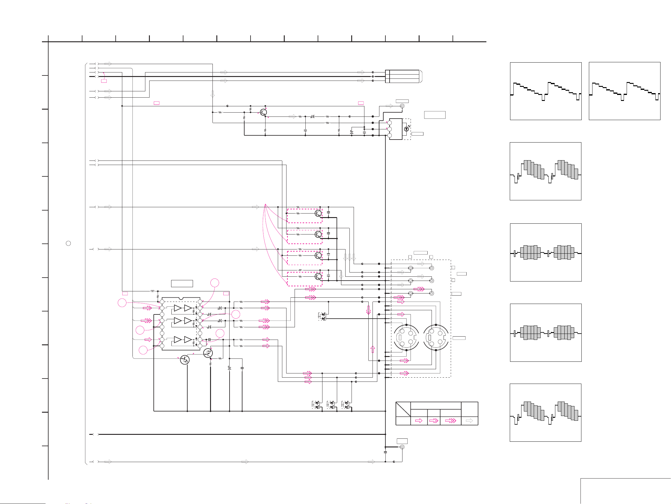
AU-222 (VIDEO BUFFER) SCHEMATIC DIAGRAM • See page 4-39 for printed wiring board.
– Ref. No.: AU-222 board; 2,000 series –
1
2 11859
4
6
7
10
DVP-F11
123
13
• Wavef orms
AU-222 BOARD(2/2)
A
B
C
D
E
F
1
AU-222 BOARD(1/2)
(SEE PAGE 4-44)
G
H
I
J
K
L
M
05
1
1 IC308 2
2
3
4
B+
5
6
B+
7
8
9
10
12345678
Q323,324
DC
ON/OFF
IC308
VIDEO BUFFER
BA7660F-E2
6dB
6dB 75
6dB 75
0
Q323
UN2213-TX
IC308
4.6
4.6
Q324
UN2111-TX
2
100u
2
2
100u
2
9 10111213141516
75
L304
100uH
B+ B+
1
VMUTE
VIDEOY
VIDEOV
R472
10k
0.4
0.6
0.6
2
VIDEOC
0.7
3
VS
FB305
R474
2200
6
C350
6.3V470u
C346
10V
C351
6.3V470u
C347
10V
C348
4
0.1u
B
2.1
4.6
R475
10k
0
R473
10k
R483
1800
R482
3900
R476
68
R477
68
5
R478
68
R479
68
R480
68
R481
68
C353
C352
0.01u
47u
B
16V
2.7
EXCEPT HK,SP,AUS,CN
4.9
Q325
2SC2412K-T-146-QR
BUFFER
2
R484
220
R485
68
R486
470
R410
1k
2SD1938(F)-T(TX).SO
FNAC MUTE
R487
470
1k
R411
2SD1938(F)-T(TX).SO
FNAC MUTE
R488
470
2SD1938(F)-T(TX).SO
FNAC MUTE
R489
470
R413
Q333
2SD1938(F)-T(TX).SO
FNAC MUTE
Q330
Q331
1kR412
Q332
1k
C356
1u
50V
C355
220p
D309
HZM6.8ZWA1TL
R490
0
R491
100
R492
100k
C357-360
:HK,SP,AUS,CN
100p
:EXCEPT HK,SP,AUS,CN
470p
C357
*
CH
C358
*
CH
C359
*
CH
C360
*
CH
B+
FB309
C361
C373
0.01u
47u
B
16V
FB310
FB311
FB312
FB313
FB314
FB315
FB316
FB306
FB307
FB308
JL304
JL305
JL306
JL307
FB317
FB318
FB319
JL315
JL308
JL309
JL310
JL311
JL312
JL313
JL314
JL316
JL317
CN306
3P
1 HPL
2 GND
3 HPR
J301
COAXIAL
1.7
1
D IN
4.9
2
VCC
3
GND
NO MARK:DVD/CD PLAY
HP-122 BOARD
CN501
(SEE PAGE 4-55)
PCM/DTS/
DOLBY DIGITAL
IC309
HVE0024
OPTICAL
2 IC308 4
1.1 Vp-p (H)
1.2 Vp-p (H)
3 IC308 7
J302
LINE OUT
1
2
R
AUDIO
L
860 mVp-p (H)
VIDEO
4 IC308 q;
G
YC
G
G
S-VIDEO
YC
G
1.8 Vp-p(H)
5 IC308 qd
6 IC308 qg
2.0 Vp-p (H)
SIGNAL PATH
VIDEO SIGNAL
Y/CHROMA
Y
J303
WOOFER
OUT
CHROMA
PB
D308
HZM6.8ZWA1TL
HZM6.8ZWA1TL
11
12
D310
D311
HZM6.8ZWA1TL
C362
100p
CH
FB320
AUDIO
SIGNAL
2.4 Vp-p (H)
4-45 4-46
VIDEO BUFFER
AU-222 (2/2)
Page 56

DVP-F11
FL-111 (IF CON) PRINTED WIRING BOARD
– Ref. No.: FL-111 board; 2,000 series –
FL-111 BOARD (SIDE A)
CN602 B-2
CN604 B-1
D604 A-3
D607 A-7
IC601 B-6
IC602 B-7
There are few cases that the part isn't mounted in this model is printed on this diagram.
TK-55
(RF/SERVO)
FR-166
(IR/FUNCTION SWITCH)
FL-111 BOARD (SIDE B)
CN603 B-7
D601 B-3
D602 B-3
D603 B-3
D606 A-3
Q604 B-2
Q605 B-2
MB-85
(SIGNAL PROCESS/SERVO)
AU-222
(AUDIO)
SW-332
(CHUCK SENSOR)
IF CON
FL-111
FL-111
(IF CON)
HP-122
(HEAD PHONE)
DC-DC Converter Unit
(SWITCHING REGULATOR)
4-47
4-48
Page 57

FL-111 (IF CON) SCHEMATIC DIAGRAM
– Ref. No.: FL-111 board; 2,000 series –
DVP-F11
1
FL-111 BOARD
A
B
MPD0102 BOARD
CN203
(SEE PAGE 4-58)
C
D
MB-85 BOARD
CN006
E
(SEE PAGE 4-29)
F
SW-332 BOARD
CN102
G
(SEE PAGE 4-14)
B601
CN602 15P
CN604
5P
2P
PCONT 1
EVER5V 2
GND 3
SW-10V 4
GND 5
XIFRST 15
XIFBUSY 14
XIFCS 13
SI0 12
SO0 11
SC0 10
GND 9
VMUTE 8
AMUTE 7
SLINK 6
A1IN 5
A1OUT 4
GND 3
MICCONT 2
+3.3V 1
4
L601
47uH
R603
6800
C601
22u
16V
B+
FB601
FB602
FB603
B-
IFBSY
IFCS
SIN
SOUT
SCLK
JL601
JL602
JL603
JL604
B+
2S101
1GND
Q604
2SD1622-S-TD
-0.1
-9.9
-10.2
-9.9
Q605
2SD1622-S-TD
Q604,605
DC-DC CONVERTER
C630
2700p
2
-0.1
3
4
6
5
C606
4.7u
35V
SCLK
SIN
SOUT
B+
IFCS
R610
IFBSY
6
D601
MA113-(TX)
T601
9
MA113-(TX)
1
MA113-(TX)
7
8
B+
R659
47k
R613
10k
R614
10k
R615
R616
10k
R617
100
R618
100
R619
100
120
33
R611
10k
C612
220p
C610
220p
B
C611
220p
B
100
R620
100
R621
MA113-(TX)
D602
D603
R612
C614
220p
C615
220p
7
B+
C603
C605
0.1u
JL607
D604
JL608
10k
B
4.9
0.1
B
B
4.8
1.6
4.9
22u
B
35V
B- B-
B+
CED
10k
10kR663
10k
10k
R660
R661
R662
10k
R665
100
5
0
000
64
0
65
LEDCS
0
66
LED_CLK
0
67
LED_DATA
0
68
P54
5
69
SELFCHK<N>
70
SCLK1
71
SOUT1
0
72
SIN1
73
AVSS
5
74
VREF
0
75
MIC_IN<N>
76
SBUSY1
77
PCHECK<N>
78
SRDY1
0
79
HKM
0
80
AN6
SEG1
SEG2
SEG4
SEG3
SEG5
-27.5
-27.50**-24.1
54
FLD955FLD856FLD757FLD658FLD559FLD460FLD361FLD262FLD163FLD0
IC601
M38B57MCH-D233FP
SEG6
SEG17
SEG18
R664
*
-27.5*-27.5
0
IC601
IF CON
1
10
D606
MA8043-H(TX)
R631
10k
SEG8
SEG7
DIG6
DIG8
DIG7
DIG5
DIG4
DIG3
DIG2
*
-24.1
-24.1
-24.1
-24.1
-24.1
FLD2242FLD2143FLD2044FLD1945FLD1846FLD1747FLD1648FLD1549FLD1450FLD1351FLD1252FLD1153FLD10
C617
0.1u
B
DIG1
-24.1
-24.1
41
FLD23
*
SEG9
*
SEG10
*
SEG11
-27.5
SEG12
-27.5
SEG13
-27.5
SEG14
*
SEG15
-20.6
SEG16
0
4.6
4.5
0
-27.7
4.3
0
0
R666
100
R667
100
R668
100
R669
100
R670
100
R671
100
R672
100
L_STBY
L_POWER
L_PLAY
L_PAUSE
L_DVD
L_VCD
FLD24
FLD25
FLD26
FLD27
FLD28
FLD29
FLD30
FLD31
40
39
38
37
36
35
34
33
32
31
30
29
28
VEE
27
26
25
L_CD
13
ND601
FLUORESCENT INDICATOR TUBE
N.C.
F2
F2
34
CED
B+
35
R653
68k
R654
68k
32
SEG17
P1
N.C.
P18
P17
28
29
30
31
SEG18
SEG1
SEG2
P6
P5
P4
P3
P2
26
27
SEG4
SEG3
P8
P7
24
25
SEG5
20
22
23
SEG8
SEG6
SEG7
DIG8
4G
5G
6G
8G
7G
17
18
19
DIG6
DIG7
DIG5
16
DIG4
3G
15
DIG3
1G13P10
2G14P9
DIG1
DIG2
17142 161185 159
N.C.
12
11
SEG9
10
SEG10
921
SEG11
P13
P12
P11
P14
5
6
7
8
SEG14
SEG13
SEG12
SEG15
18123
F1
F1
P15
P16
2
1
4
SEG16
• Wavef orm
1 IC601 qf
C608
0.1u
B
H
C609
0.1u
B
10kR606
10k
10k
R626
R627
B+
R629
I
J
K
L
05
ECHO-VOL1MICCTRL2AN33AN24AN15AN06STATUS7FRRST<N>8IR9RESET<N>10VMUTE11AMUTE<N>12VSS13XIN14XOUT15VCC16JOG_CCW17JOG_CW18A1OUT19P4320P4221KBC_IN22INT023P-CONT
5
505
5
0500000
3.2
10k
10k
R607
R604
100R628
1k
100R630
R633
10k
10k
10k
10k
R636
R634
R635
100
4700
R637
R638
C622
C620
C619
0.01u
B
220p
220p
B
JL610
B
R673
100
C624
0.1u
B
C625
0.1u
B
C623
220p
B
R639
100k
D607
1SS355TE-17
2.4
2.1
10k
10k
R640
R641
B+
X601
4MHz
5
Vcc
N.C.2SUB3GND
1
10k
10k
10k
R642
R645
R643
C626
220p
B
54.9
4
VOUT
IC602
PST9140NL
IC602
POWER-ON
RESET
24
0000000
4.9
10k
10k
R647
R646
B+
3.9 Vp-p (4 MHz)
R648
100
R650
10k
B+
NO MARK:DVD/CD PLAY
R652
R651
10k
*:IMPOSSIBLE TO MEASURE THE
VOLTAGE AT THE MARKED POINTS.
R655
10k
10k
R675
0
CN603 12P
LPLAY1
LPAUSE2
LCD3
LVCD4
LDVD5
GND6
LSTBY7
LPOW8
IR9
BT10
B+
EVER5V11
GND12
FR-166 BOARD
CN701
(SEE PAGE 4-53)
4-49 4-50
IF CON
FL-111
Page 58

DVP-F11
FR-166 (IR/FUNCTION SWITCH) PRINTED WIRING BOARD
– Ref. No.: FR-166 board; 2,000 series –
There are few cases that the part isn't mounted in this model is printed on this diagram.
FR-166 BOARD (SIDE B)
CN701 B-7
D701 A-8
D702 A-5
D703 A-4
D704 A-5
D705 B-2
D706 B-3
IC701 A-1
TK-55
(RF/SERVO)
FR-166
(IR/FUNCTION SWITCH)
MB-85
(SIGNAL PROCESS/SERVO)
AU-222
(AUDIO)
SW-332
(CHUCK SENSOR)
FL-111
(IF CON)
HP-122
(HEAD PHONE)
IR/FUNCTION SWITCH
FR-166
DC-DC Converter Unit
(SWITCHING REGULATOR)
4-51 4-52
Page 59

FR-166 (IR/FUNCTION SWITCH) SCHEMATIC DIAGRAM
– Ref. No.: FR-166 board; 2,000 series –
DVP-F11
1
2859
3
4
6
7
10
FR-166 BOARD
A
B
RED
SPR-325MVW
(ON/STANDBY)
3
GND
2
VCC
1
OUT
GP1U27X
D701
IC701
R709
220
GREEN
IC701
REMOTE
COMMANDER
RECEIVER
R710
220
D702
SLR-342DCT31
R711
220
D703
SLR-342DCT31
DVD VIDEO CD CD
R712
220
D704
SLR-342DCT31
R713
220
D705
SLR-342DCT31
R714
100
D706
SLR-342MCT31
C
D
E
FL-111 BOARD
CN603
(SEE PAGE 4-50)
CN701 12P
LPLAY 1
LPAUSE 2
LCD 3
LVCD 4
LDVD 5
GND 6
LSTBY 7
LPOW 8
IR 9
BT 10
EVER5V 11
GND 12
R708
680
B+
L701
R701
S701
10k
/
B+
S702
S703
S704
S705
R702
3300
R703
4700
R704
12k
R705
47k
22uH
C702
10u
16V
C701
0.1u
R706
100
B
4.9
4.9
F
05
NO MARK:DVD/CD PLAY
IR/FUNCTION SWITCH
4-53 4-54
FR-166
Page 60

DVP-F11
HP-122 (HEADPHONE) PRINTED WIRING BOARD AND SCHEMATIC DIAGRAM
– Ref. No.: HP-122 board; 2,000 series –
There are few cases that the part isn't mounted in this model is printed on this diagram.
1
A
HP-122 BOARD
B
AU-222 BOARD
CN306
(SEE PAGE 4-46)
RV501
PHONES LEVEL
RV501
500/500
3PCN501
HPL 1
GND 2
HPR 3
05
C
D501
HZM6.8ZWA1TL
43
HZM6.8ZWA1TL
D502
C501
4700p
625
R502
47
FB501
R501
47
C502
4700p
B
R503
FB502
47
B
R504
47
SIGNAL PATH
AUDIO
SIGNAL
PB
FB503
JL501
JL502
JL503
J501
PHONES
7
HEADPHONE
HP-122
FR-166
(IR/FUNCTION SWITCH)
SW-332
(CHUCK SENSOR)
4-55 4-56
TK-55
(RF/SERVO)
FL-111
(IF CON)
MB-85
(SIGNAL PROCESS/SERVO)
AU-222
(AUDIO)
DC-DC Converter Unit
(SWITCHING REGULATOR)
HP-122
(HEAD PHONE)
Page 61

DVP-F11
MPD0102 (SWITCHING REGULATOR) PRINTED WIRING BOARD AND SCHEMATIC DIAGRAM
– Ref. No.: MPD0102 board; 6,000 series –
MPD0102
A
05
BOARD
E
C
B
E
E
C
C
B
B
12345 6
SDG
3
1
41
3
E
C
1
B
There are few cases that the part isn't mounted in this model is printed on this diagram.
+
–
DC IN 10.5V
SDG
B
C
E
B
C
E
1-418-669- 11
MPD0102 BOARD
CN201 A-1
CN202 A-2
CN203 A-1
D201 A-6
D221 A-5
D251 A-3
D261 A-3
D262 A-1
D271 A-3
D272 A-1
D292 A-2
IC251 A-2
IC271 A-3
IC281 A-2
Q201 A-5
Q202 A-5
Q221 A-5
Q261 A-3
Q291 A-1
Q292 A-1
Q293 A-1
Q294 A-1
1
MPD0102 BOARD
J201
+
–
A
DC IN 10.5V
D201
ERB83-006
B
C
D
05
L202
23456789
IC281
EVER+5V
REG
9.3
3
Q292
2SC1740S
POWER
CONTROL
0.7
R292
10K
R271
1K
IC281
uPC78L05
0.7
Q291
2SJ378
S
4.9
B+
R281
22
0.6
B-
B+
D292
ERA15-006
C252
+
47uF
35V
B+
0
L261
10uH
10.4
0
B+
R295
10K
0
R294
2.7K
B+
BEA291
R221
33K
L201
10uH
B+
Q201
2SK2232
10.4
SWITCH
5.3
S
D221
1SS133
Q221
2SC1740S
7.6
SWITCH
0
R223
C201
+
220uF
35V
33K
R201
10K
R219
R205
10K
C210
0.033uF
10
5.3
R206
180
R212
22K
Q202
2SC1741AS
SWITCH
– 0.4
C209
4700p
R211
22K
R208
33k
B+
B+ SWITCH
B+
10.5
C263
0.1uF
1
PQ05RD11
R264
470
R265
3.3K
R266
10K
R293
100K
IC251
3 4
C272
+
47uF
35V
2
Q293
2SC1740S
B+ SWITCH
D272
HZ22
R268
1K
D262
HZS12
C291
+
47uF
35V
B+
T201
D251
ERB83-006
C251
330uF
16V
D261
2FWJ42N
D271
ERA83-006
B+
+
5.6
B+
– 0.4
R267
100
+
C261
470uF
16V
C271
+
56uF
35V
B-
SW+5V
R261
1K
5.1
2SA933S
SWITCH
R262
1K
4.5
IC271
TA76431S
IC271
SHUNT REG
IC251
REG
Q261
R263
2.5
5.6
1K
L271
10uH
2
R291
10K
R272
1
0
R296
1K
5
C281
+
47uF
35V
C262
+
47uF
35V
Q294
2SC1740S
POWER
CONTROL
1K
NO MARK : E-E MODE
B+
B+
B-
CN202
6P
B+
1
EVER5V
B+
2
SW+5V
3
GND
B+
4
SW+10V
5
GND
B-
6
SW–10V
CN201
7P
B+
1
SW+10V
B+
2
SW+10V
3
GND
4
GND
B+
5
SW+5V
6
SW+3.3V
B+
7
SW+3.3V
CN203
5P
1
PCONT
B+
2
EVER+5V
3
GND
B-
4
SW–10V
5
GND
AU-222 BOARD
CN303
(SEE PAGE 4-43)
MB-85 BOARD
CN001
(SEE PAGE 4-37)
FL-111 BOARD
B601
(SEE PAGE 4-49)
4-57 4-58 E
SWITCHING REGULATOR
MPD0102
Page 62

SECTION 5
Pin No. Pin name I/O Function
68 EOP0 I Not used
69 AVCC - Power supply
70 AVRH - Reference power supply (+3.3V)
71 AGND - Ground
72 AN0 I Set of mode 0
73 AN1 I Set of mode 1
74 AN2 I Set of mode 2
75 AN3 I Set of mode 3 (fixed at “H”)
76 SI0 I Serial data input from IF CON and EEPROM
77 SO0 O Serial data output to IF CON and EEPROM
78 SC0 O Serial clock output to IF CON and EEPROM
79 SI1 I Serial bus 1 (for data input)
80 SO1 O Serial bus 1 (for data output)
81 SI2 I Serial bus 2 (for data input)
82 SO2 O Serial bus 2 (for data output)
83 PF7 O Reset signal output
84 DACK1 O Output of DMA-ACK 0 to AV DEC
85 DACK0 O Output of DMA-ACK 1 to AV DEC
86 DREQ1 I Input of DMA-REQ 0 from AV DEC
87 DREQ0 I Input of DMA-REQ 1 from AV DE C
88 INT3 I Input of interrupt from HGA
89 SC1 O Serial clock output
90 GND - Ground
91 X1 O Clock output (12.5MHz)
92 X0 I Clock input (12.5MHz)
93 VCC5 - Power supply
94 INT1 I Input of interrupt ARP and SERVO DSP
95 INT0 I Input of interrupt from AV DE C
96 PB0 I Rear panel lime input select (“H”: DISC “L”: EXT)
97 PB1 O Chip select signal to IF CON
98 PB2 O Chip select signal to DAC (Lt and Rt)
99 PB3 O Chip select signal to DAC (L and R)
100 PB4 O DVD/CD select (“H”: 44.1kHz “L”: 48kHz)
5-1. SYSTEM CONTROL PIN FUNCTION (MB-85 BOARD IC202)
Pin No. Pin name I/O Function
1 PB5 O Analog filter gain control
2 PB6 O VES gain control “H”: VES
3 PB7 O Rear CH boost control “H”: rear boost
4 VCC3 - Power supply
5 CLK O CPU clock out (25 MHz)
6 CS5 O Not used
7 CS4 O Chip select signal for ARP, SERVO DSP and HGA
8 CS3 O Chip select signal for SDRAM and AV DEC
9 CS2 O Chip select signal for REG and AV DEC
10 CS1 O Chip select signal for external SRAM
11 CS0 O Chip select signal for external FLASH ROM
12 NMI I Not used (fixed at “H”)
13 HST I Not used (fixed at “H”)
14 RST I Reset signal input from IF CON
15 GND - Ground
16 MD0 I Input of mode select 0 (fixed at “1”)
17 MD1 I Input of mode select 1 (fixed at “0”)
18 MD2 I Input of mode select 2 (fixed at “0”)
19 RDY I Wait signal input
20 P81 I Test terminal (fixed at “H”)
21 P82 I Test terminal (fixed at “L”)
22 RD O Read enable signal output
23 WR0 O High byte write enable signal output (16 bit and 8 bit)
24 WR1 O Low byte write enable signal output (16 bit only)
25-32 D16-D23 I/O Data bus D0-D7 (16 bit)
33-39 D24-D30 I/O Data bus D8-D14 (16 bit), D0-D6 (8 bit)
40 GND - Ground
41 D31 I/O Data bus D15 (16 bit), D7 (8 bit)
42 A00 O Address bus A0
43 VCC5 - Power supply
44-64 A01-A21 O Address bus A1-A21
65 GND - Ground
66 P66 O PLL IC control output “H”: DOUBLE
67 P67 I DIAG mode signal input “L”: DIAG
IC PIN FUNCTION DESCRIPTION
DVP-F11
5-1
5-1 E
Page 63

SECTION 6
TEST MODE
DVP-F11
6-1. GENERAL DESCRIPTION
The T est Mode allows you to make diagnosis and adjustment easily using the remote commander and monitor TV. The instructions,
diagnostic results, etc. are given on the on-screen display (OSD).
6-2. STARTING TEST MODE
Press [TITLE], [CLEAR], [POWER] buttons on the remote commander in this order with the power of main unit in OFF status,
and the T est Mode starts, then the menu shown below will be displayed on the TV screen. At the bottom of menu screen, the model
name and revision number are displayed.
To execute each function, select the desired menu and press its
number on the remote commander.
To exit from the Test Mode, press the POWER button.
Test Mode Menu
0. Syscon Diagnosis
1. Drive Auto Adjustment
2. Drive Manual Operation
3. Mecha Aging
4. Emergency History
5. Version Information
6. Video Level Adjustment
Exit: Power Key
_
Model : DPX12xxxx
Revision : 1.xxxx
6-3. SYSCON DIAGNOSIS
The same contents as board detail check by serial interface can be
checked from the remote commander.
On the T est Mode Menu screen, press [0] k e y on the remote commander, and the following check menu will be displayed.
### Syscon Diagnosis ###
Diag All Check
No. 2 Version
2-3. ROM Check Sum
Check Sum = xxxx
Press NEXT Key to Continue
Press PREV Key to Repeat
_
For the ROM Check, the check sum calculated by the Syscon is
output, and therefore you must compare it with the specified value
for confirmation.
Following the message, press [NEXT] key to go to the next item,
or [PREV] ke y to repeat the same check again. To quit the diagnosis and return to the Check Menu screen, press [STOP] or
[ENTER] key. If an err or occurred, the diagnosis is suspended
and the error code is displayed as shown below.
### Syscon Diagnosis ###
3-3. EEPROM Check
Error 03: EEPROM Write/Reed N
Address : 00000001
Write Data : 2492
Read Data : 2490
Press NEXT Key to Continue
Press PREV Key to Repeat
_
Press [STOP] key to quit the diagnosis, or [PREV] key to repeat
the same item where an error occurred, or [NEXT] key to continue
the check from the item next to faulty item.
### Syscon Diagnosis ###
Check Menu
0. Quit
1. All
2. Version
3. Peripheral
4. Servo
5. Supply
6. AV Decoder
7. Video
8. Audio
_
0. Quit
Quit the Syscon Diagnosis and return to the Test Mode Menu.
1. All
All items continuous check
This menu checks all diagnostic items continuously . Normally , all
items are checked successively one after another automatically
unless an error is found, but at a certain item that requires judgment through a visual check to the result, the following screen is
displayed for the key entry.
Submenu
Selecting 2 and subsequent items calls the submenu screen of each
item.
For example, if “5. Supply” is selected, the following submenu
will be displayed.
### Syscon Diagnosis ###
Check Menu
No. 5 Supply
0. Quit
1. All
2. ARP Register Check
3. ARP to RAM Data Bus
4. ARP to RAM Address Bus
5. ARP RAM Check
_
0. Quit
Quit the submenu and return to the main menu.
1. All
All submenu items continuous check
This menu checks 2 and subsequent items successively. At the
item where visual check is required for judgment or an error occurred, the checking is suspended and the message is output for
key entry. Nor mally, all items are checked successively one after
another automatically unless an error is found.
6-1
Page 64

Selecting 2 and subsequent items executes respective menus and
outputs the results.
For the contents of each submenu, see “Check Items List”.
General Description of Checking Method
2. Version
(2-2) Revision
ROM revision number is displayed.
Error: Not detected.
The revision number defined in the source file of ROM
(IC205 or IC206) is displayed with four digits.
4. Servo
(4-2) Servo DSP Check
Data write → read, and accord check
Error 12: Read data discord
Data 0x9249, 0x2942, 0x4294 are written to the address
0x602 of RAM in the Servo DSP (IC701), then read and
checked.
(4-3) DSP Driver Test
Test signal data → DSP Driver
Error: Not detected.
(2-3) ROM Check Sum
Check sum is calculated.
Error: Not detected.
The 8-bit data are added at addresses 0x000F0000 ~
0x002EFFFF of ROM (IC205 or IC206) and the result is
displayed with 4-digit hexadecimal number. Error is not
detected. Compare the result with the specified value.
(2-4) Model Type
Model code is displayed.
Error: Not detected.
The model code read from EEPROM (IC201) is displayed
with 2-digit hexadecimal number.
Hong Kong, Singapore 8 1
Australian 8 3
EXCEPT Hong Kong,
Singapore, Australian, Chinese
Chinese 8 4
(2-5) Region
Region code is displayed.
Error: Not detected.
The region code determined from the model code is displayed.
3. Peripheral
(3-2) Gate Array Check
Data write → read, and accord check
Error 02: Gate array write/read discord
Data 0x00~0xFF are written to the address 0xF of GA
(IC601), then read and checked if they accord.
(3-3) EEPROM Check
Data write → read, and accord check
Error 03: EEPROM write/read discord
Data 0x9249, 0x2942, 0x4294 are written to addresses
0x00~0xFF of EEPROM (IC201), then read and checked.
Before writing, the data are saved, then after checking, they
are written to restore the contents of EEPROM.
Model Type
82
Caution: Do not conduct this test with a mechanical deck
connected.
The maximum voltage is applied to the Servo Driver IC
(IC801, IC802). If mechanical deck is connected, the motor and optics could be damaged. Disconnect mechanical
deck following the output message, then enter specified 4or 5-digit number from the remote commander, and press
the [ENTER]. The test is conducted only when the input
data accord. Check the output level, then press the [NEXT]
to finish the test.
This test is skipped if “All” is selected.
Supplement: How to disconnect mechanical deck
Disconnect flat cables connected to the CN002
and CN003 of MB-85 board. Also, disconnect
harness from the CN011.
5. Supply
Caution: Do not conduct this check with a mechanical deck con-
nected.
An access is made to the stream supply and servo control IC (IC303) and external RAM (IC304) using check
data. If mechanical deck is connected, the motor and
optics could be damaged. This check is also executed by
the “All” menu item.
Supplement: How to disconnect mechanical deck
Disconnect flat cables connected to the CN002 and
CN003 of MB-85 board. Also, disconnect harness
from the CN011.
(5-2) ARP Register Check
Data write → read, and accord check
Error 08: ARP register write, and read data discord
Data 0x00 to 0xFF are written to the TMAX register (address 0xC6) in ARP (IC303), then they are r ead and checked.
(5-3) ARP to RAM Data Bus
Data write → read, and accord check
Error 09: ARP ←→ RAM data bus error
Data 0x0001 to 0x8000 where one bit each is set to 1 are
written to the address 0 of RAM (IC304) connected to the
ARP (IC303) through the bus, then they are read and
checked. In case of discord, written bit pattern and read
data are displayed. If data where multiple bits are 1 are
read, the bits concerned may touch each other. Further, if
data where certain bit is always 1 or 0 regardless of written
data, the line could be disconnected or shorted.
6-2
Page 65

(5-4) ARP to RAM Address Bus
Data write → other address read discord check
Error 10: ARP → RAM address bus error
Caution: Address and data display in case of an error is
different from the display of other diagnosis (de-
scribed later).
Before starting the test, all addresses of RAM (IC304) are
cleared to 0x0000.
First, 0xA55A is written to the address 0x00000, and the
address data are read and checked from addresses 0x00001
to 0x80000 while shifting 1 bit each. Next, the data at that
address is cleared, and it is written to the address 0x00001,
and read and checked in the same manner. This check is
repeated up to the address 0x80000 while shifting the address data by 1 bit each.
If data other than 0 is read at the addresses except written
address, an error is given because all addresses were already cleared to 0. In this check, the error display pattern is
different from that of other diagnosis; read data, written
address, and read address are displayed in this order. Ho wever , the message uses same template, and accordingly exchange Address and Data when reading. T he following display, for example,
### Syscon Diagnosis ###
5-4. ARP to RAM Address Bus
Error 10: ARP - RAM Address B
Address : 0000A55A
Write Data : 00000000
Read Data : 00080000
Press NEXT Key to Continue
Press PREV Key to Repeat
_
6. AV Decoder
(6-2) 1930 RAM
Data write → read, and accord check
Error 13: AVD RAM read data discord
The program code data stored in ROM (IC205 or IC206)
are copied to all areas of RAM (IC402, IC403) connected
to the AVD (IC401) through the bus, then they are read and
checked if they accord. Further, the same test is conducted
once again with the data where all bits are inverted between
1 and 0. If discord is detected, faulty address, written data,
and read data are displayed following the error code 13,
and the test is suspended.
(6-3) 1930 SP
ROM → AVD RAM → Video OUT
Error: Not detected.
The data including sub picture streams in ROM (IC205 or
IC206) are transferred to the RAM (IC402, IC403) in AVD
(IC401), and output as video signals from the AVD (IC401).
They are output from all video terminals (Composite, Y/C)
except EURO AV terminal.
7. Video
(7-2) Color Bar
AVD color bar command write → Video OUT
Error: Not detected.
The command is transferred to the AVD, and the color bar
signals are output from video terminals.
They are output from all video terminals (Composite, Y/C)
except EURO AV terminal.
8. Audio
(8-2) ARP → 1930
Error 14: ARP → 1930 video NG
15: ARP → 1930 audio NG
shows the data 0xA55A was read from address 0x00080000
though it was written to the address 0x00000000. This implies that these addresses are in the form of shadow. Also,
if the read data is not 0xA55A, another error will be present.
(5-5) ARP RAM Check
Data write → read, and accord check
Error 11: ARP RAM read data discord
The program code data stored in ROM are copied to all
areas of RAM (IC304) connected to the ARP (IC303)
through the bus, then they are read and checked if they accord. If the detail check was selected initially, the data are
written to all areas and read, then the same test is conducted
once again with the data where all bits are inverted between
1 and 0. If discord is detected, faulty address, written data,
and read data are displayed following the error code 11,
and the test is suspended.
(8-3) Test Tone
A pink noise signal is output from the AVD (IC401) through
optical coaxial digital terminal and analog audio terminal.
Error: Not detected.
All channels → 2ch Left → 2ch Right → Front Left →
Front Right → Rear Left → Rear Right → Center → Sub
Woofer are checked in this order.
Caution: Sub Woofer is checked only for low-frequency
components, and no sound will be heard unless a
proper super woofer is connected.
6-3
Page 66

Check Items List
2) Version
(2-2) Revision
(2-3) ROM Check Sum
(2-4) Model Type
(2-5) Region
3) Peripheral
(3-2) Gate Array Check
(3-3) EEPROM Check
4) Servo
(4-2) Servo DSP Check
(4-3) DSP Driver Test
5) Supply
(5-2) ARP Register Check
(5-3) ARP to RAM Data Bus
(5-4) ARP to RAM Address Bus
(5-5) ARP RAM Check
6) AV Decoder
(6-2) 1930 RAM
(6-3) 1930 SP
7) Video
(7-2) Color Bar
Error Codes List
00: Error not detected
01: RAM write/read data discord
02: Gate array NG
03: EEPROM NG
08: ARP register read data discord
09: ARP ←→ RAM data bus error
10: ARP ←→ RAM address bus error
11: ARP RAM read data discord
12: Servo DSP NG
13: 1930 SDRAM NG
14: ARP → 1930 video NG
15: ARP → 1930 audio NG
16: 1910 UCODE download NG
17: System call error (function not supported)
18: System call error (parameter error)
19: System call error (illegal ID number)
20: System call error (time out)
90: Error occurred
91: User verification NG
92: Diagnosis cancelled
8) Audio
(8-2) ARP → 1930
(8-3) Test Tone
6-4
Page 67

6-4. DRIVE AUTO ADJUSTMENT
On the T est Mode Menu screen, press [1] k e y on the remote commander, and the drive auto adjustment menu will be displayed.
1. DVD-SL (single layer)
Select [1], insert DVD single layer disc, and press [ENTER] key,
and the adjustment will be made through the following steps, then
adjusted values will be written to the EEPROM.
## Drive Auto Adjustment ##
Adjustment Menu
0. ALL
1. DVD-SL
2. CD
3. DVD-DL
4. SACD
Exit: RETURN
Normally, [0] is selected to adjust DVD (single layer), CD, DVD
(dual layer), and SACD in this order. But, individual items can be
adjusted for the case where adjustment is suspended due to an
error. In this mode, the adjustment can be made easily through the
operation following the message displayed on the screen.
The disc used for adjustment must be the one specified for adjustment. However, for SACD disc, use the player with initial data if
the disc is not available.
0. ALL
Select [0] and press [ENTER] key, and the servo set data in
EEPROM will be initialized. Then, 1. DVD-SL disc, 2. CD disc,
3. DVD-DL disc, and 4. SACD disc are adjusted in this order.
Each time one disc was adjusted, it is ejected. Replace it with the
specified disc following the message. Though the message to confirm whether discs other than SACD disc are adjusted is not displayed, you can finish the adjustment if pressing the
ton. During adjustment of each disc, the measurement for disc
type judgment is made. As automatic adjustment does not judge
the disc type unlike conventional models, take care not to insert
wrong type discs. Also, do not give a shock during adjustment.
[STOP] but-
DVD Single Layer Disc Adjustment Steps
1. SLED TILT Reset
2. Disc Check Memory SL
3. Wait 300 msec
4. Set Disc Type SL
5. LD ON
6. Spdl Start
7. Wait 1 sec
8. Focus Servo ON 0
9. Auto Track Offset Adjust
10. CLVA ON
11. Wait 500 msec
12. Tracking ON
13. Wait 1 sec
14. Sled ON
15. Check CLV Lock
16. Auto LFO Adjust
17. Auto Focus Offset Adjust
18. Auto Tilt Position Adjust
19. Auto Focus Gain Adjust
20. Auto Focus Offset Adjust
21. EQ Boost Adjust
22. Auto LFO Adjust
23. Auto Track Gain Adjust
Search Check
24. 32Tj Fwd
25. 32Tj Rev
26. 500Tj Fwd
27. 500Tj Rev
28. All Servo Stop
29. Eep Copy Loop Filter Offset
6-5
Page 68

2. CD
Select [2], insert CD disc, and press [ENTER] ke y , and the adjustment will be made through the following steps, then adjusted values will be written to the EEPROM.
3. DVD-DL (dual layer)
Select [3], insert DVD dual layer disc, and press [ENTER] key,
and the adjustment will be made through the following steps, then
adjusted values will be written to the EEPROM.
CD Adjustment Steps
1. Sled Tilt Rest
2. Disc Check Memory CD
3. Wait 500 msec
4. Set Disc Type CD
5. LD ON
6. Spdl Start
7. Wait 500 msec
8. Focus Servo ON 0
9. Auto Track Offset Adjust
10. CLVA ON
11. Wait 500 msec
12. Tracking ON
13. (TC Display Start)
14. Wait 1 sec
15. Jitter Display Start
16. Sled ON
17. Check CLV ON
18. Auto LFO Adjust
19. Auto Focus Offset Adjust
20.
21. Auto Focus Gain Adjust
22. Auto Focus Offset Adjust
23. Eq Boost Adjust
24. Auto LFO Adjust
25. Auto Track Gain Adjust
Search Check
26. 32Tj Fwd
27. 32Tj Rev
28. 500Tj Fwd
29. 500Tj Rev
30. All Servo Stop
DVD Dual Layer Disc Adjustment Steps
1. Sled Tilt Reset
2. Disc Check Memory DL
3. Wait 500 msec
4. Set Disc Type DL
5. LD ON
6. Spdl Start
7. Wait 1 sec
Layer 1 Adjust
8. Focus Servo ON 0
9. Auto Track Offset Adjust
10. Clva ON
11. Wait 500 msec
12. Tracking ON
13. Wait 500 msec
14. Sled ON
15. Check CLV Lock
16. Auto Loop Filter Offset Auto Focus Adjust
17.
18. Auto Focus Gain Adjust
19. Auto Focus Offset Adjust
20. Eq Boost Adjust
21. Auto Loop Filter Offset
22. Auto Track Gain Adjust
Search Check
23. 32Tj Fwd
24. 32Tj Rev
25. 500Tj Fwd
26. 500Tj Rev
Layer 0 Adjust
27. Fj (L1 -> L0)
28. Auto Track Offset Adjust L0
29. Clva ON
30. Wait 500 msec
31. Tracking ON
32. Wait 500 msec
33. Sled ON
34. Check CLV Lock
35. Auto Focus Filter Offset
36. Auto Focus Adjust
37.
38. Auto Focus Gain Adjust
39. Auto Focus Offset Adjust
40. Eq Boost Adjust
41. Auto Loop Filter Offset
42. Auto Track Gain Adjust
Search Check
43. 32Tj Fwd
44. 32Tj Rev
45. 500Tj fwd
46. 500Tj Rev
Layer Jump Check
47. Lj (L0 -> L1)
48. Lj (L1 -> L0)
49. All Servo Stop
6-6
Page 69

4. SACD
Select [4], insert SACD disc, and press [ENTER] key, and the
adjustment will be made through the following steps, then adjusted
values will be written to the EEPROM. However, if SACD disc is
not available, use the player with initial data, skipping the SACD
adjustment. In this case, you can finish the adjustment if pressing
the [STOP] button.
6-5. DRIVE MANUAL OPERATION
On the T est Mode Menu screen, select [2], and the manual operation menu will be displayed. For the manual operation, each servo
on/off control and adjustment can be executed manually.
## Drive Manual Operation ##
SACD Adjustment Steps
1. Sled Tilt Reset
2. Set Disc Type CD
3. LD ON
4. Spdl Start
5. Wait 500 msec
6. Focus Servo ON 0
7. Auto track Offset Adjust
8.
9. CLVA ON
10. Wait 500 msec
11. Tracking ON
12. Wait 1 sec
13. Sled ON
14. Check CLV ON
15. Auto Focus Offset Adjust
17.
18. Auto Focus Gain Adjust
19. Auto Focus Offset Adjust
20. Eq Boost Adjust
21. Auto LFO Adjust
22. Auto Track Gain Adjust
23. 32Tj Fwd
24. 32Tj Rev
25. 500Tj Fwd
26. 500Tj Rev
27. All Servo Stop
1. Disc type
Operation Menu
2. Servo Control
3. Track/Layer Jump
4. Manual Adjustment
5. Auto Adjustment
6. Memory Check
0. Disc Check Memory
Exit: Return
In using the manual operation menu, take care of the following
points. These commands do not provide protection, thus requiring
correct operation. The sector address or time code field is displayed when a disc is loaded.
1. Set correctly the disc type to be used on the Disc Type
screen.
The disc type must be set after a disc was loaded.
The set disc type is cleared when the tray is opened.
2. After power ON, if the Drive Manual Operation was selected, first perform “Reset SLED TILT” by opening 1.
Disc Type screen.
3. In case of an alarm, immediately press the [STOP] button to stop the servo operation, and turn the power OFF.
Basic operation (controllable from front panel or remote commander)
[POWER] Power OFF
[STOP] Servo stop
[OPEN/CLOSE] Stop+Eject/Loading
[RETURN] Return to Operation Menu or Test Mode
Menu
[NEXT], [PREV] Transition between sub modes of menu
[1] to [9], [0] Selection of menu items
Cursor UP/DOWN Increase/Decrease in manually adjusted
value
6-7
Page 70

0. Disc Check Memory
Disc Check
1. SL Disc Check
2. CD Disc Check
3. DL Disc Check
0. Reset SLED TILT
1. Disc Type Auto Check
Disc Type
2. DVD SL 12 cm
3. DVD DL 12 cm
4. CD 12cm
5. SACD 12 cm
6. DVD SL 8 cm
7. DVD DL 8 cm
8. CD 8 cm
9. SACD 8 cm
0. Reset SLED TILT
TC. : : EMG. 00
CD 12 cm
Display when CD 12cm disc was selected
On this screen, the mirror time is measured to judge the disc and it
is written to the EEPROM. First load DVD SL disc and press [1],
next load CD disc and press [2], and finally load DVD DL disc
and press [3].
The adjustment must be executed more than once after default
data were written. External vibration or shock to the player must
not be given. Reference value for DVD is from 10 to 20, and for
CD, from 28 to 4F.
Check that the value of CD is larger than that of DVD.
When those values are beyond a range perform this adjustment
again.
From this screen, you can go to another mode by pressing [NEXT]
or [PREV] key , but you cannot enter this mode from another mode.
You can enter this mode from the Operation Menu screen only.
1. Disc Type
Disc Type
1. Disc Type Auto Check
2. DVD SL 12 cm
3. DVD DL 12 cm
4. CD 12cm
5. SACD 12 cm
6. DVD SL 8 cm
7. DVD DL 8 cm
8. CD 8 cm
9. SACD 8 cm
0. Reset SLED TILT
EMG. 00
[0] Reset SLED TILT Reset the Sled and Tilt to initial posi-
tion.
[1] Disk Type Check Judge automatically the loaded disc. As
the judged result is displayed at the bottom of screen, make sure that it is correct.
If Disc Check Memory menu has not
been executed after EEPROM default
setting, the disc type cannot be judged.
In this case, return to the initial menu
and make a check for three types of
discs (SL, DL, CD).
[2] to [9] Select the loaded disc. The adjusted
value is written to the address of selected disc. No further entry is necessary if [1] was selected.
2. Servo Control
Servo Control
1. LD Off R.Sled FWD
2. SP Off L.Sled REV
3. Focus Off
4. TRK. Off
5. Sled Off
6. CLVA Off
7. FCS. Srch Off
On this screen, select the disc type. To select the disc type, press
the number of the loaded disc. The selected disc type is displayed
at the bottom. Selecting [1] automatically selects and displays the
disc type. In case of wrong display, retry “Disc Check Memory”.
Also, opening the tray causes the set disc type to be cleared. In
this case, set the disc type again after loading.
In performing manual operation, the disc type must be set.
Once the disc type has been selected, the sector address or time
code display field will appear as shown below. T hese values are
displayed when PLL is locked.
Disc Type
1. Disc Type Auto Check
2. DVD SL 12 cm
3. DVD DL 12 cm
4. CD 12cm
5. SACD 12 cm
6. DVD SL 8 cm
7. DVD DL 8 cm
8. CD 8 cm
9. SACD 8 cm
0. Reset SLED TILT
SA. SI. EMG. 00
DVD SL 12 cm
Display when DVD SL 12cm disc was selected
0. Reset SLED TILT
SA. SI. EMG. 00
DVD SL 12 cm
On this screen, the servo on/off control necessary for replay is
executed. Normally, turn on each servo from 1 sequentially and
when CLV A is turned on, the usual trace mode becomes acti ve . In
the trace mode, DVD sector address or CD time code is displayed.
This is not displayed where the spindle is not locked.
The spindle could run overriding the control if the spindle system
is faulty or RF is not present. In such a case, do not operate CL VA.
6-8
Page 71

[0] Reset SLED TILT Reset the Sled and Tilt to initial posi-
tion.
[1] LD Turn ON/OFF the laser.
[2] SP Turn ON/OFF the spindle.
6-6. MECHA AGING
### Mecha Aging ###
[3] Focus Search the focus and turn on the focus.
[4] TRK Turn ON/OFF the tracking servo.
[5] Sled Turn ON/OFF the sled servo.
[6] CLVA Turn ON/OFF normal servo of spindle
servo.
[7] FCS. Srch A p p l y same voltage as that of focus
search to the focus drive to check the
focus drive system.
→ Sled FWD Move the sled outward. Perform this
operation with the tracking servo turned
off.
← Sled REV Move the sled inward. Perform this op-
eration with the tracking servo turned
off.
Tilt UP Move the tilt upward.
↑
Tilt DOWN Move the tilt downward.
↓
The following menus are normally not used.
3. Track/Layer Jump
Press OPEN key
Abort: STOP key
On the Test Mode Men u screen, selecting [3] executes the aging
of mechanism. First, open the tray and load a disc. Press the [PLAY]
key , and the aging will start. When the tray is closed, the disc type
and size are judged and displayed. During aging, the repeat cycle
is displayed. Aging can be aborted at any time by pressing the
[STOP] key. After the operation has stopped, unload the disc and
press again the [STOP] key or the [RETURN] key to return to the
Test Mode Menu.
6-7. EMERGENCY HISTORY
### MEG. History ###
Laser Hours CD xxxxxxxh
DVD xxxxxxxh
1. 00 00 00 00 00 00 00 00
00 00 00 00 00 00 00 00
2. 00 00 00 00 00 00 00 00
00 00 00 00 00 00 00 00
4. Manual Adjustment
5. Auto Adjustment
The persons who do not know well about these menus should not
use them.
6. Memory Check
EEPROM DATA
CD – DVD –
ID No. 00 SACD SL L0 L1
Focus Gain xx xx xx xx xx
TRK. Gain xx xx xx xx xx
Focus Offset xx xx xx xx xx
TRK. Offset xx xx xx xx xx
L. F. Offset xx xx xx xx xx
EQ Boost xx xx xx xx xx
Jitter xx xx xx xx xx
Mirror Time xx xx xx xx xx
_
CLEAR: Default Set
This screen displays current servo adjusted data stored in the
EEPROM. Though adjusted data can be initialized with the
[CLEAR] key, they cannot be restored after initialization.
So, before clearing, make a note of the adjusted data.
For reference, the drive has been designed so that the gain center
value is 20 and offset value is 80. Other values will be in a range
of 10 to 80. If extreme value such as 00 or FF is set, adjustment
will be faulty. In such a case, check for disc scratch or cable disconnection, then perform adjustment again.
Select: 1 – 9 Scroll: UP/DOWN
(1: Last EMG.) Exit: Return
On the Test Mode Menu screen, selecting [4] displays the information such as servo emergency history. The history information
from last 1 up to 10 can be scrolled with ↑key or↓key . Also,
specific information can be displayed by directly entering that
number with ten keys.
The upper two lines display the laser ON total hours. Data below
minutes are omitted.
Clearing History Information
Clearing laser hours
Press [DISPLAY] and [CLEAR] keys in this order.
Both CD and DVD data are cleared.
Clearing emergency history
Press [TITLE] and [CLEAR] keys in this order.
Initializing set up data
Press [DVD] and [CLEAR] keys in this order.
The data have been initialized when “Set Up Initialized” message is displayed. The EMG. History screen will be restored
soon.
6-9
Page 72
How to see Emergency History
6-8. VERSION INFORMATION
31.12
2
1 : Emergency Code
2 : Don’t Care
These codes are used for verification of software designing.
3 : Historical order 1 to 9
Emergency Codes List
10: Comm unica tion to IC001 (TK-55 board) failed.
11: Each servo for focus, tracking, and spindle is unlocked.
12: Communication to EEPROM, IC201 (MB-85 board) failed.
13: Writing of hours meter data to EEPROM, IC201 (MB-85
board) failed.
14: Communication to Servo DSP IC701 (MB-85 board) failed,
or Servo DSP is faulty.
20: Initializa tion of tilt servo and sled servo failed. They are not
placed in the initial position.
21: Tilt servo operation error
22: Syscon made a request to move the tilt servo to wrong posi-
tion.
23: Sled servo operation error
24: Syscon made a request to move the sled servo to wrong posi-
tion.
30: Tracking balance adjustment error
31: Tracking gain adjustment error
32: Focus balance adjustment error
33: Focus bias adjustment error
34: Focus gain adjustment error
35: Tilt servo adjustment error
36: RF equalizer adjustment error
37: RF group delay adjustment error
38: Jitter value after adaptive servo operation is too large.
40: Focus servo does not operate.
41: With a dual layer (DL) disc, focus jump failed.50: CLV
(spindle) servo does not operate.
51: Spindle does not stop.
60: With a DVD disc, Syscon made a request to seek nonexistent
address.
61: With a CD disc, Syscon made a request to seek nonexistent
address.
62: With a CD disc, Syscon made a request to seek nonexistent
track No. and index No.
63: With a DVD disc, seeking of target address failed.
64: With a CD disc, seeking of target address failed.
65: With a CD disc, seeking of target index failed.
70: With a DVD disc, physical information data could not be read.
71: With a CD disc, TOC data could not be read.
80: Disc type judgment failed.
81: As disc type judgment failed, retry was repeated.
82: As disc type judgment failed, a measurement error occurred.
83: Disc type could not be judged within the specified time.
84: Illegal command code was received from Syscon.
85: Illegal command was received from Syscon.
## Version Information ##
IF con. Ver. x. xxx (xxxx)
Group 00
SYScon. Ver. x. xxx (xxxx)
Model xx
Region 0x
SW1 ??
SW2 ??
Exit: RETURN
On the Test Mode Menu screen, selecting [5] displays the ROM
version and region code.
The parenthesized hexadecimal number in version field is
checksum value of ROM.
6-9. VIDEO LEVEL ADJUSTMENT
On the Test Mode Menu screen, selecting [6] displays color bars
for video level adjustment. During display of color bars, OSD disappears but the menu screen will be restored if pressing any key.
Measurement point :LINE OUT VIDEO
(75 Ω terminating resistance)
Measuring instrument: Oscilloscope
Adjustment device : RV401 on MB-85 board
Specified value : 1.0 ± 0.02 Vp-p
1.0 ± 0.02 Vp-p
6-10
Page 73

6-10. IF CON SELF DIAGNOSTIC FUNCTION
1. FRONT BOARD TEST MODE
The front board test mode is the IF CON self diagnostic mode.
The IF CON can diagnose the functions of the front panel boards
that the IF CON controls. Normally, the IF CON makes a serial
communication with the SYSTEM CONTROL and operates following thecommands from the SYSTEM CONTROL, but in the
Test mode, the IF CON operates independently from the SYSTEM CONTROL.
In the Test mode, the following functions can be checked.
1. Button function
2. Remocon receiving function
3. SYSTEM CONTROL-IF CON serial communication
4. Direct search dial function
5. Click shuttle function
6. Fluorescent display tube lighting check
Grid check
Anode check
7. LED control function
In the Test mode, the set operates same as usual, except voltage
monitoring, communication monitoring, display of fluorescent
display tube, and LED control.
1. The routine that monitors +3.3 V (PCONT) of MB-85 board is
not provided.
2. The monitoring timer for serial communication with the SYSTEM CONTROL is not provided. The set is not placed in the
Standby mode, even if the communication with SYSTEM
CONTROL is normal.
3. Display of fluorescent display tube (normally, display is made
following the commands from SYSTEM CONTROL)
4. LED control (normally, control is made following the commands from SYSTEM CONTROL)
2. HOW TO ENTER THE TEST MODE
The set must be placed in the Standby mode (red LED lights up).
In the standby mode, press the [RETURN] key , then the [SET UP]
key on the remocon while pressing the [STOP] button on the set,
so that the set enters the test mode.
When the Test mode becomes active, the automatic display sequence of the FL display tube starts.
1. LEDs and FL display tube all light up for about 5 seconds.
2. Then, the prototypical model name is displayed.
(This model name is a typical name of the series. As the button arrangement varies depending on the model, make sure
the difference.)
Display Model
DPX-1290 DVP-F11
3. Last updating date of the program is displayed.
Example: 981211
4. Following the “GRID TEST” display, odd grids and ev en grids
are blinking alternately (3 times).
5. Following the “ANODE TEST” display, even anodes and odd
anodes are blinking alternately (3 times). For the FL display
tube type A, e ven and odd numeric parts of music calendar are
blinking alternately (3 times).
6. All light-up mode restores.
Steps 1 through 6 are repeated. (Refer to “FLD Auto Test Operation” on page 6-12)
3. HOW TO EXIT FROM THE TEST MODE
Press the [POWER] buttons on the set and Remocon, and the FL
display tube turns off and the Standby mode is restored where
only the red POWER LED lights up. This is the case where the
SYSTEM CONTROL and IF CON are communicating normally.
To forcibly activate the Standby mode, press the [POWER] button together with the [STOP] button.
6-11
Page 74

FLD Auto Test Operation
1 FLD all light up (5 sec)
ANGLE
DTS
PBC
NTSC
2 TEST START display (2 sec) This is not displayed after second and subsequent tests.
ANGLE
DTS
PBC
NTSC
3 Model display (2 sec)
ANGLE
DTS
PBC
NTSC
A- B
A- B
TEST ST
A- B
DPX1290
TRACK CHAP
TRACK CHAP
TRACK CHAP
HOUR MIN SEC
HOUR MIN SEC
HOUR MIN SEC
TITLE
TITLE
TITLE
Note: Prototypical model name of the series is displayed.
4 Date display (2 sec) Program updating date is displayed.
ANGLE
DTS
PBC
NTSC
5 GRID TEST start display (1 sec)
ANGLE
DTS
PBC
NTSC
A- B
990719
A- B
GRID TE
TRACK CHAP
TRACK CHAP
HOUR MIN SEC
HOUR MIN SEC
TITLE
TITLE
6-12
Page 75

6 FLD odd grids light up (0.7 sec)
ANGLE
DTS
PBC
NTSC
7 FLD even grids light up (0.7 sec)
ANGLE
DTS
PBC
NTSC
8 FLD ANODE TEST display No.1 (1 sec)
ANGLE
DTS
PBC
NTSC
A- B
A- B
A- B
ANODE T
TRACK CHAP
TRACK CHAP
TRACK CHAP
HOUR MIN SEC
HOUR MIN SEC
HOUR MIN SEC
TITLE
TITLE
Note: Displays of 6 and 7 are repeated three times.
TITLE
9 FLD even anodes light up (0.7 sec)
ANGLE
DTS
PBC
NTSC
0 FLD odd anodes light up (0.7 sec)
ANGLE
DTS
PBC
NTSC
A- B
A- B
Hence, the operations of 1 through 0 arerepeated.
However, 2 is not displayed after the second and subsequent tests.
TRACK CHAP
TRACK CHAP
HOUR MIN SEC
HOUR MIN SEC
TITLE
Note: Also, even anodes of alphanumeric section light up.
TITLE
Note: Also, odd anodes of alphanumeric section light up.
Note: Displays of 9 and 0 are repeated three times.
6-13
Page 76

4. DESCRIPTION OF IF CON FUNCTION CHECK
MODE
1. Button Function
In the Test mode, press any button (except [POWER] button) on
the set. This operation terminates the automatic display test mode
of the FL display tube. During the time that the button is pressed,
the function name of the pressed button is displayed on the FL
display tube, and “NOTHING” is displayed if releasing the button. For the button names displayed, refer to the following table.
For the illuminated button (LED built in), it turns on and of f alter nately each time it is pressed. For the multi-channel LED (blue
LED), it blinks when the “RETURN” button is pressed because
its dedicated button is not provided.
Input V olta ge [V]
1 0 POWER
2 0.65 OPEN/CLOSE
3 1.24 PLAY
4 1.88 STOP
5 2.41 PAUSE
The direction buttons are used to enter special modes.
: FL display tube grid check
↑
: LED check
↓
← : Direct search dial check
→ : FL display tube anode check
IC601: Pin No. (Signal)
Pin 6 (AN0)
4. Direct Search Dial
The grid X part displays images that rotate. At the same time, the
numbers on music calendar shift toward the direction in which the
direct search dial was rotated.
(Though this is displayed on the models which do not have the
dial, it does not function because of no dial.)
5. Click Shuttle
Whether the IF CON can judge the rotation of click shuttle is
checked.In the following grid check and anode check, if the part
that lights up is shifted as the click shuttle rotates, the function is
normal.
6. Display of Fluorescent Display Tube
Use this mode when checking the FL display tube precisely, though
the FL display tube is roughly checked in the auto display mode.
Press simultaneously the [STOP] and [PLAY] buttons on the set,
so that the FL display tube can all be lighted up.
The buttons are all checked with the voltage at the A/D port. The
reference voltage of A/D port is e ver 5V. The voltage is calculated
at 10bit accuracy and evaluated whether same voltag e can be obtained in two-time operations to eliminate the chattering.
For the button check by the IF CON, a dead zone is provided, and
if voltage in the dead zone is entered, “IGNORE” is displayed.
2. Remocon Receiving Function
Upon reception of a code from the Remocon when “NOTHING”
is displayed, the function name of Remocon code is displayed on
the FL display tube. The codes that can be received are DVD category codes only. The “DISPLAY” on Remocon functions to
change over the function name display and the code display . In the
code display mode, “REM NO xx” is displayed. A xx part is the
received code in Hex notation. It is FF when a Remocon code is
not received.
3. SYSTEM CONTROL-IF CON Serial Communication
Normally, two-way communication at 24ms interval is made between IF CON and SYSTEM CONTROL. Whether this communication is carried out normally can be checked easily. When
“NOTHING” is displayed, OFF display of “ANGLE”, “DTS”,
“PBC”, and “NTSC” characters on the left side of FL display tube
indicates that a serial communication with the SYSTEM CONTROL is carried out normally. ON display of these characters indicates that the communication with the SYSTEM CONTROL is
not made.
However, the communication is not made for several seconds after the T est mode became activ e (until MB-85 board is initialized),
and these characters may turn on. This status is normal.
6-14
Page 77

3G
P2
1G 2G 3G 4G 5G 6G 7G 8G
Dp
a
f
h
g
e
r
p
n
scm
d
j
k
b
( 2G~8G )
P1
P3
P4
P5
P6
P7
P8
P9
P10
P11
P12
P13
P14
P15
P16
P17
P18
h
a
2G
a
1G
j
k
b
f
m
s
g
c
e
n
p
r
d
Dp
h
j
k
b
f
m
s
g
c
e
n
p
r
d
Dp
h
a
j
k
b
f
m
s
g
c
e
n
p
r
d
Dp
h
a
j
k
b
f
m
s
g
c
e
n
p
r
d
Dp
h
a
j
k
b
f
m
s
g
c
e
n
p
r
d
Dp
h
a
j
k
b
f
m
s
g
c
e
n
p
r
d
Dp
h
a
j
k
b
f
m
s
g
c
e
n
p
r
d
4G 5G 6G 7G 8G
(Grid)
(Anode)
6-15
Page 78

7. Grid Check (↑ button: Grid Check Mode)
In this mode, arbitrary one grid of FL display tube lights up. (The
anodes of the grid concerned all light up.) To shift the grids, use
the click shuttle on the set. For the models not having the click
shuttle, the DVD Remocon having the click shuttle can be used
instead.
During this mode, any one grid always lights up.
8. Anode Check (→ button: Anode Check Mode)
In this mode, arbitrary one anode of FL display tube lights up.
(All grids of the anode concerned all light up.)
Staring from P1, rotate the click shuttle clockwise, and the anodes
shift such as P2, P3 .... The anodes return to P1 following the last
anode. During this mode, one anode of all grids always lights up.
For the models not having the click shuttle, the DVD Remocon
having the click shuttle can be used instead.
9. LED Control
In this mode, LEDs, one by one, light up by pressing the↓button.
The “CD”, “VIDEO CD” and “DVD” LEDs on the set can be
controlled with the [STOP] button.
Each time the [STOP] button is pressed, CD → VIDEO CD →
DVD → CD, VIDEO CD, DVD light up → CD, VIDEO CD , DVD
go off are repeated.
5. TROUBLESHOO TING
1. Test Mode is not activated
With the set assembled in the front panel, the Test mode does not
become active if any button w as pressed by an y reason.Under this
condition, the power is not turned on even in the normal status.
(The set is kept in Standby status = Red LED is kept on) Not only
the buttons are inactive, but also a signal from Remocon is not
accepted. To check this condition, with the self check port (pin yl
of IF CON) kept in “Low” status, supply the A C po wer , so that the
Test mode is f orcibly activated. On the board, short the lands where
SELF is printed. The IF CON checks the self check port only after
the power on reset (only when AC is supplied; not in Standby status). If any button was pressed, the button name should be displayed on the FL display tube. Though no button is pressed this
time, display of other than NOTHING implies that the button was
pressed. However, the set will go in Standby status immediately
unless the FFC (pin qj) connected to the MB-85 board is disconnected in advance.
2. Power is not turned on
1 Red (STANDBY) LED does not light up when AC was sup-
plied. The power (EVER 5 V) is not supplied.
X201 is oscillating.
Loose connection of the connector between FL board and FR
board.
2 Red (ST ANDBY) LED is kept on though PO WER b utton was
pressed. Any button is kept pressed.
PCHECK (IF CON pin uj) is over 0.1 V.
3 Green LED lights up when POWER button was pressed, but
red LED lights up again after several seconds. PCHECK (IF
CON pin uj) is abnormal. (Slow rise time from 0.1 V to 1.5 V.
Voltage must be less than 1.5 V)
SYSTEM CONTROL does not operate normally.
6-16
6-16 E
Page 79

SECTION 7
ELECTRICAL ADJUSTMENT
DVP-F11
In making adjustment, refer to 7-3. Adjustment
Related Parts Arrangement.
Note: During diagnostic check, the characters and color bars can
be seen only with the NTSC monitor. Therefore, for diagnostic check, use the monitor that supports both NTSC and
PAL modes.
Use the reference disc for P AL for check, and use the refer ence disc for NTSC for adjustment.
This section describes procedures and instructions necessary for
adjusting electrical circuits in this set.
Instruments required:
1) Color monitor TV
2) Oscilloscope 1 or 2 phenomena, band width over 100 MHz,
with delay mode
3) Frequency counter (over 8 digits)
4) Digital voltmeter
5) Standard commander (RMT-D109E/D109O)
6) DVD reference disc
HLX-501 (J-6090-071-A) (dual layer) (NTSC)
HLX-503 (J-6090-069-A) (single layer) (NTSC)
HLX-504 (J-6090-088-A) (single layer) (NTSC)
HLX-505 (J-6090-089-A) (dual layer) (NTSC)
HLX-506 (J-6090-077-A) (single layer) (PAL)
HLX-507 (J-6090-078-A)(dual layer) (PAL)
7) SACD reference disc
HLXA-509 (J-6090-090-A)
7-1. POWER SUPPLY ADJUSTMENT
1. MPD0102 Board
Mode E-E
Instrument Digital voltmeter
+5 V Check
Test point CN201 pin 5
Specification 5.0 ± 0.2 Vdc
+3.3 V Check
Test point CN201 pin 7
Specification 3.3 ± 0.2 Vdc
EVER+5 V Check
Test point CN203 pin 2
Specification 5.0 ± 0.2 Vdc
P_CONT Check
Test point CN203 pin 1
Specification 4V – 5 Vdc
+10 V Check
Test point CN201 pin 1
Specification 9.5 Vdc
–10 V Check
Test point CN203 pin 4
Specification –10.0 ± 1.0 Vdc
+1.5
–0.5
Checking method:
1) Confirm that each voltage satisfies the specification.
7-1
Page 80

7-2. ADJUSTMENT OF VIDEO SYSTEM
1. Video Level Adjustment (MB-85 BOARD)
<Purpose>
This adjustment is made to satisfy the NTSC standard, and if not
adjusted correctly, the brightness will be too large or small.
Mode Video level adjustment in test mode
Signal Color bars
Test point
Instrument Oscilloscope
Adjusting element RV401
Specification 1.0 ± 0.02 Vp-p
Adjusting method:
1) In the test mode initial menu “6” Video Level Adjustment, set
so that color bars are generated.
2) Adjust the RV401 to attain 1.0 ± 0.02 Vp-p.
LINE OUT (VIDEO) connector
(75 Ω terminated)
3. Checking S Video Output S-C (MB-85 BOARD)
<Purpose>
This checks whether the S-C satisfies the NTSC Standard. If it is
not correct, the colors will be too dark or light.
Mode Video level adjustment in test mode
Signal Color bars
Test point
Instrument Oscilloscope
Specification
Checking method:
1) In the test mode initial menu “6” Video Level Adjustment, set
so that color bars are generated.
2) Confirm that the S-C burst is 300 ± 100 mVp-p.
S VIDEO OUT (S-C) connector
(75 Ω terminated)
286 ± 50 mVp-p (NTSC)
300 ± 100 mVp-p (PAL)
300 ± 100 mVp-p
1.0 ± 0.02 Vp-p
Figure 7-1
2. S-terminal Output Check (MB-85 BOARD)
<Purpose>
Check S-terminal video output. If it is incorrect, pictures will not
be displayed correctly in spite of connection to the TV with a Sterminal cable.
Mode Video level adjustment in test mode
Signal Color bars
Test point
Instrument Oscilloscope
Specification 1.0 ± 0.1 Vp-p
Checking method:
1) In the test mode initial menu “6” Video Level Adjustment, set
so that color bars are generated.
2) Confirm that the S-Y level is 1.0 ± 0.1 Vp-p.
S VIDEO OUT (S-Y) connector
(75 Ω terminated)
Figure 7-3
Figure 7-2
1.0 ± 0.1 Vp-p
7-2
Page 81
7-3. ADJUSTMENT RELATED PARTS ARRANGEMENT
12
2728
CN005
RV401
VIDEO LEVEL ADJ
CN202CN201
CN203
1
1716
5
MB-85 BOARD (SIDE A)
MPD0102 BOARD (SIDE A)
7-4 E
Page 82

8-1. EXPLODED VIEWS
12
13
2
7
3
1
4
5
14
15
7
3
6
7
8
9
7
9
11
10
not
supplied
not
supplied
not
supplied
7
DVP-F11
SECTION 8
REPAIR PARTS LIST
NOTE:
• -XX and -X mean standardized parts, so they may
have some difference from the original one.
• Items marked “*” are not stocked since they are
seldom required for routine service. Some delay
should be anticipated when ordering these items.
• Abbreviation
AUS: Australian model
CN : Chinese model
HK : Hong Kong model
SP : Singapore model
• The mechanical parts with no reference number in
the exploded views are not supplied.
• Accessories and packing materials are given in the
last of the electrical parts list.
8-1-1. CASE AND FRONT PANEL ASSEMBLIES
The components identified by mark
0 or dotted line with mark 0 are
critical for safety.
Replace only with part number specified.
Ref. No. Part No. Description Remark
1 X-3949-958-4 PANEL ASSY, FRONT
* 2 A-6065-378-A FR-166 BOARD, COMPLETE
3 3-979-433-11 SCREW (+P2.6), TAPPING
* 4 A-6065-377-A FL-111 BOARD, COMPLETE
5 3-057-522-01 KNOB, HP VOLUME
* 6 A-6065-379-A HP-122 BOARD, COMPLETE
7 3-970-608-01 SUMITITE (B3), +BV
8 3-057-500-01 CASE (UPPER) (EXCEPT HK, SP, CN)
8 3-057-500-12 CASE (UPPER) (HK, SP, CN)
9 3-970-608-51 SUMITITE (B3), +BV
Ref. No. Part No. Description Remark
10 3-055-791-01 SUMITITE (B3) (RING), +BV
11 X-3950-084-2 CASE (LOWER) ASSY
12 1-418-508-21 COMMANDER, STANDARD (RMT-D109O/S)
(EXCEPT HK, SP, CN)
12 1-418-508-31 COMMANDER, STANDARD (RMT-D109E/S)
(HK, SP, CN)
13 3-053-633-01 COVER, BATTERY
(for RMT-D109O/S, D109E/S)
14 3-950-989-01 NUT (M7), HEXAGON
15 X-3950-213-1 FILM ASSY, SHILD
8-1
Page 83
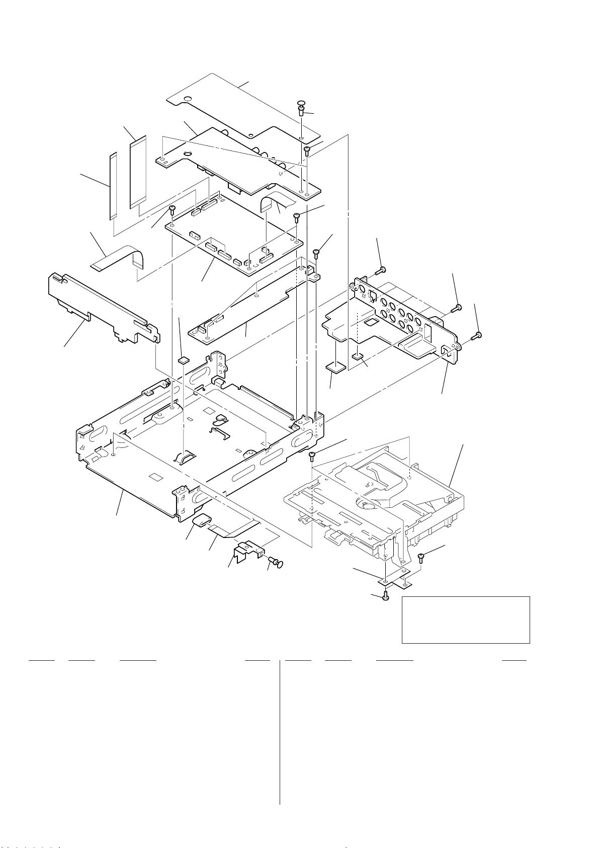
8-1-2. CHASSIS ASSEMBLY
k
64
51
54
52
55
53
56
60
not
supplied
61
59
65
53
53
53
not
supplied
62
62
62
not
supplied
63
not supplied
66
57
67
Ref. No. Part No. Description Remark
51 3-057-505-01 PLATE, HEAT INSULATING
52 1-791-670-11 CABLE, FLEXIBLE FLAT (FMT-27)
53 3-055-791-01 SUMITITE (B3) (RING), +BV
54 1-791-668-11 CABLE, FLEXIBLE FLAT (FMA-17)
55 1-791-669-11 CABLE, FLEXIBLE FLAT (FMA-18)
65
58
Mechanism dec
58
not supplied
58
The components identified by mark
0 or dotted line with mark 0 are
critical for safety.
Replace only with part number specified.
Ref. No. Part No. Description Remark
* 60 A-6065-384-A MB-85 BOARD, COMPLETE (HK, SP)
* 60 A-6065-385-A MB-85 BOARD, COMPLETE (AUS)
* 60 A-6065-390-A MB-85 BOARD, COMPLETE (E32)
* 60 A-6065-414-A MB-85 BOARD, COMPLETE (CN)
0 61 1-418-669-11 CONVERTER UNIT, DC-DC
* 56 A-6065-376-A AU-222 BOARD, COMPLETE
(EXCEPT HK, SP, AUS, CN)
* 56 A-6065-383-A AU-222 BOARD, COMPLETE (HK, SP, AUS, CN)
57 1-791-672-11 CABLE, FLEXIBLE FLAT (FMS-12)
58 3-970-608-01 SUMITITE (B3), +BV
59 1-791-671-11 CABLE, FLEXIBLE FLAT (FMF-38)
* 60 A-6065-375-A MB-85 BOARD, COMPLETE (CED, UK)
62 3-970-608-51 SUMITITE (B3), +BV
63 3-057-504-01 PANEL, REAR
64 3-058-362-01 COVER, AU
65 3-531-576-01 RIVET
66 1-543-950-11 CORE, FERRITE
67 3-058-026-01 HOLDER (SW)
8-2
Page 84

8-1-3. MECHANISM DECK ASSEMBLY-1
not
supplied
104
107
not
supplied
105
103
106
108
not
supplied
109
110
116
not
supplied
111
101
102
105
not
supplied
112
113
112
115
112
114
113
113
The components identified by mark
0 or dotted line with mark 0 are
critical for safety.
Replace only with part number specified.
101 A-6062-251-A CHASSIS (TOP) BLOCK ASSY
102 4-981-286-01 SCREW (M1.7X2) (IB LOCK)
103 4-989-134-01 SPRING (R), TORSION
104 4-989-135-01 SPRING (L), TORSION
105 4-989-987-01 BEARING (SLIDE)
106 3-059-234-01 SPRING (CENTERING), COIL
107 X-3950-387-1 LEVER (CENTERING R) ASSY
108 3-932-755-01 SCREW (M1.7X2.2)
Ref. No. Part No. Description RemarkRef. No. Part No. Description Remark
109 3-057-574-01 PLATE, YOKE
110 3-057-573-01 PLATE, CHUCK
111 X-3950-204-1 ARM ASSY, CHUCKING
112 3-057-023-01 INSULATOR (RB)
113 3-057-582-01 SCREW, INSULATOR
0 114 8-820-081-09 OPTICAL PICK-UP KHM-220AAA/J1RP
* 115 A-6065-381-A TK-55 BOARD, COMPLETE
116 7-621-759-45 PSW, 2.6X6
8-3
Page 85

8-1-4. MECHANISM DECK ASSEMBLY-2
155
not
supplied
153
not
supplied
160
154
164
161
not
supplied
M001
165
158
163
S001
170
166
167
not
supplied
168
169
154
153
not
supplied
152
156
151
151 4-989-170-01 SPRING (ROLLER), TENSION
152 A-6062-261-A ARM BLOCK ASSY, ROLLER
153 4-991-241-01 WASHER
154 4-989-163-01 GEAR (ROLLER A)
155 4-989-169-03 GEAR (ROLLER B)
159
157
162
158
158
Ref. No. Part No. Description RemarkRef. No. Part No. Description Remark
162 X-3949-966-1 CHASSIS (FRONT) ASSY
163 3-060-386-01 GEAR (LD B)
164 3-317-552-71 SCREW (M1.7)
165 3-057-568-01 SLIDER, CAM
166 4-993-986-01 SCREW (2) (P TITE), (+) P TAPPING
156 4-989-162-01 WHEEL (LD), WORM
157 4-989-164-02 GEAR (LD A)
158 3-377-719-11 WASHER, POLYETHYLENE
159 4-989-186-01 BELT, ROLLER
160 4-989-185-02 PULLEY, ROLLER
161 4-989-184-02 PULLEY, MOTOR
167 1-960-020-11 HARNESS (ST-117)
168 4-989-188-01 SPRING (CAM SLIDER), TENSION
169 X-3949-967-1 FRAME ASSY, MAIN
170 7-685-133-19 SCREW (DIA. 2.6) (IT3B)
M001 A-6062-252-A MOTOR ASSY, LD (LOADING)
S001 1-570-771-21 SWITCH (CHUCK SENSOR)
8-4
Page 86

8-2. ELECTRICAL PARTS LIST
AU-222
NOTE:
• Due to standardization, replacements in the
parts list may be different from the parts specified in the diagrams or the components used
on the set.
• -XX and -X mean standardized parts, so they
may have some difference from the original
one.
• RESISTORS
All resistors are in ohms.
METAL: Metal-film resistor.
METAL OXIDE: Metal oxide-film resistor.
F: nonflammable
• Abbreviation
AUS : Australian model
CN : Chinese model
HK : Hong Kong model
SP : Singapore model
Ref. No. Part No. Description Remark Ref. No. Part No. Description Remark
* A-6065-376-A AU-222 BOARD, COMPLETE
* A-6065-383-A AU-222 BOARD, COMPLETE (HK, SP, AUS, CN)
***********************
< CAPACITOR >
C301 1-163-233-11 CERAMIC CHIP 18PF 5% 50V
C302 1-163-233-11 CERAMIC CHIP 18PF 5% 50V
C304 1-126-926-11 ELECT 1000uF 20% 10V
C305 1-115-339-11 CERAMIC CHIP 0.1uF 10% 50V
C306 1-163-239-11 CERAMIC CHIP 33PF 5% 50V
C307 1-163-239-11 CERAMIC CHIP 33PF 5% 50V
C308 1-163-239-11 CERAMIC CHIP 33PF 5% 50V
C312 1-163-009-11 CERAMIC CHIP 0.001uF 10% 50V
C313 1-115-339-11 CERAMIC CHIP 0.1uF 10% 50V
C314 1-104-665-11 ELECT 100uF 20% 10V
• Items marked “*” are not stocked since they
are seldom required for routine service.
Some delay should be anticipated when ordering these items.
• SEMICONDUCTORS
In each case, u: µ, for example:
uA. . : µA. . uPA. . : µPA. .
uPB. . : µPB. . uPC. . : µPC. .
uPD. . : µPD. .
• CAPACITORS
uF: µF
• COILS
uH: µH
• Not all of the parts for DC-DC CONVERTER
UNIT (MPD0102) are listed.
C342 1-104-665-11 ELECT 100uF 20% 10V
(EXCEPT HK, SP, AUS, CN)
(Ref.No. 2,000 Series)
C345 1-104-665-11 ELECT 100uF 20% 10V
C346 1-104-665-11 ELECT 100uF 20% 10V
C347 1-104-665-11 ELECT 100uF 20% 10V
C348 1-164-004-11 CERAMIC CHIP 0.1uF 10% 25V
C350 1-126-935-11 ELECT 470uF 20% 6.3V
C351 1-126-935-11 ELECT 470uF 20% 6.3V
C352 1-104-664-11 ELECT 47uF 20% 16V
C353 1-163-021-91 CERAMIC CHIP 0.01uF 10% 50V
C355 1-163-259-91 CERAMIC CHIP 220PF 5% 50V
C356 1-126-960-11 ELECT 1uF 20% 50V
C357 1-163-133-00 CERAMIC CHIP 470PF 5% 50V
C357 1-163-251-11 CERAMIC CHIP 100PF 5% 50V
C358 1-163-133-00 CERAMIC CHIP 470PF 5% 50V
The components identified by
mark 0 or dotted line with mark
0 are critical for safety.
Replace only with part number
specified.
When indicating parts by reference
number, please include the board.
(EXCEPT HK, SP, AUS, CN)
(HK, SP, AUS, CN)
(EXCEPT HK, SP, AUS, CN)
C315 1-163-021-91 CERAMIC CHIP 0.01uF 10% 50V
C316 1-104-665-11 ELECT 100uF 20% 10V
C317 1-104-664-11 ELECT 47uF 20% 16V
C318 1-104-664-11 ELECT 47uF 20% 16V
C319 1-163-021-91 CERAMIC CHIP 0.01uF 10% 50V
C320 1-104-664-11 ELECT 47uF 20% 16V
C321 1-163-131-00 CERAMIC CHIP 390PF 5% 50V
C322 1-163-131-00 CERAMIC CHIP 390PF 5% 50V
C323 1-163-145-00 CERAMIC CHIP 0.0015uF 5% 50V
C324 1-163-021-91 CERAMIC CHIP 0.01uF 10% 50V
C325 1-163-021-91 CERAMIC CHIP 0.01uF 10% 50V
C326 1-163-133-00 CERAMIC CHIP 470PF 5% 50V
C327 1-163-020-00 CERAMIC CHIP 0.0082uF 10% 50V
C328 1-163-021-91 CERAMIC CHIP 0.01uF 10% 50V
C329 1-130-491-00 MYLAR 0.047uF 5% 50V
C330 1-163-133-00 CERAMIC CHIP 470PF 5% 50V
C331 1-163-021-91 CERAMIC CHIP 0.01uF 10% 50V
C332 1-163-021-91 CERAMIC CHIP 0.01uF 10% 50V
C334 1-136-170-00 MYLAR 0.27uF 5% 50V
C335 1-163-021-91 CERAMIC CHIP 0.01uF 10% 50V
C336 1-104-664-11 ELECT 47uF 20% 16V
C337 1-136-850-11 MYLAR 0.1uF 5% 63V
C338 1-104-664-11 ELECT 47uF 20% 16V
C339 1-104-664-11 ELECT 47uF 20% 16V
C340 1-136-850-11 MYLAR 0.1uF 5% 63V
C358 1-163-251-11 CERAMIC CHIP 100PF 5% 50V
(HK, SP, AUS, CN)
C359 1-163-133-00 CERAMIC CHIP 470PF 5% 50V
(EXCEPT HK, SP, AUS, CN)
C359 1-163-251-11 CERAMIC CHIP 100PF 5% 50V
(HK, SP, AUS, CN)
C360 1-163-133-00 CERAMIC CHIP 470PF 5% 50V
(EXCEPT HK, SP, AUS, CN)
C360 1-163-251-11 CERAMIC CHIP 100PF 5% 50V
(HK, SP, AUS, CN)
C361 1-163-021-91 CERAMIC CHIP 0.01uF 10% 50V
C362 1-163-251-11 CERAMIC CHIP 100PF 5% 50V
C365 1-163-021-91 CERAMIC CHIP 0.01uF 10% 50V
C366 1-163-021-91 CERAMIC CHIP 0.01uF 10% 50V
C367 1-164-346-11 CERAMIC CHIP 1uF 16V
C368 1-164-346-11 CERAMIC CHIP 1uF 16V
C369 1-164-346-11 CERAMIC CHIP 1uF 16V
C371 1-163-021-91 CERAMIC CHIP 0.01uF 10% 50V
C372 1-163-021-91 CERAMIC CHIP 0.01uF 10% 50V
C373 1-104-664-11 ELECT 47uF 20% 16V
< CONNECTOR >
CN301 1-785-698-11 CONNECTOR, FFC/FPC 28P
CN302 1-785-695-11 CONNECTOR, FFC/FPC 13P
CN303 1-573-733-11 PIN, CONNECTOR 6P
CN306 1-506-482-11 PIN, CONNECTOR 3P
C341 1-104-664-11 ELECT 47uF 20% 16V
8-5
Page 87

AU-222
Ref. No. Part No. Description Remark Ref. No. Part No. Description Remark
< DIODE >
D301 8-719-988-61 DIODE 1SS355TE-17
D302 8-719-988-61 DIODE 1SS355TE-17
D304 8-719-988-61 DIODE 1SS355TE-17
D305 8-719-988-61 DIODE 1SS355TE-17
D306 8-719-988-61 DIODE 1SS355TE-17
D308 8-719-071-15 DIODE HZM6.8ZWA1TL
D309 8-719-071-15 DIODE HZM6.8ZWA1TL
D310 8-719-071-15 DIODE HZM6.8ZWA1TL
D311 8-719-071-15 DIODE HZM6.8ZWA1TL
Q306 8-729-424-08 TRANSISTOR UN2111-TX
Q307 8-729-424-08 TRANSISTOR UN2111-TX
Q311 8-729-046-97 TRANSISTOR 2SD1938 (F)-T (TX).SO
Q314 8-729-046-97 TRANSISTOR 2SD1938 (F)-T (TX).SO
Q317 8-729-046-97 TRANSISTOR 2SD1938 (F)-T (TX).SO
Q318 8-729-046-97 TRANSISTOR 2SD1938 (F)-T (TX).SO
Q319 8-729-046-97 TRANSISTOR 2SD1938 (F)-T (TX).SO
Q320 8-729-046-97 TRANSISTOR 2SD1938 (F)-T (TX).SO
Q321 8-729-046-97 TRANSISTOR 2SD1938 (F)-T (TX).SO
Q322 8-729-046-97 TRANSISTOR 2SD1938 (F)-T (TX).SO
< FERRITE BEAD >
FB301 1-414-553-11 FERRITE 0uH
FB302 1-414-553-11 FERRITE 0uH
FB303 1-414-553-11 FERRITE 0uH
FB304 1-414-553-11 FERRITE 0uH
FB305 1-414-135-11 FERRITE 0uH
FB306 1-414-553-11 FERRITE 0uH
FB307 1-414-553-11 FERRITE 0uH
FB308 1-414-553-11 FERRITE 0uH
FB309 1-414-553-11 FERRITE 0uH
FB310 1-414-553-11 FERRITE 0uH
FB311 1-414-553-11 FERRITE 0uH
FB312 1-414-553-11 FERRITE 0uH
FB313 1-414-553-11 FERRITE 0uH
FB314 1-414-553-11 FERRITE 0uH
FB315 1-414-553-11 FERRITE 0uH
FB316 1-414-553-11 FERRITE 0uH
FB317 1-414-553-11 FERRITE 0uH
FB318 1-414-553-11 FERRITE 0uH
FB319 1-414-553-11 FERRITE 0uH
FB320 1-414-553-11 FERRITE 0uH
< IC >
IC301 8-759-288-53 IC LA5617
IC303 8-759-909-71 IC BA4558F-E2
IC304 8-759-909-71 IC BA4558F-E2
IC305 8-759-909-71 IC BA4558F-E2
IC306 8-759-525-25 IC BU4052BCF-E2
IC307 8-759-909-71 IC BA4558F-E2
IC308 8-759-563-79 IC BA7660F-E2
IC309 8-749-016-00 IC HVE0024 (OPTICAL)
IC310 8-759-242-64 IC TC4W53F (TE12R)
< JACK >
Q323 8-729-421-19 TRANSISTOR UN2213-TX
Q324 8-729-424-08 TRANSISTOR UN2111-TX
Q325 8-729-120-28 TRANSISTOR 2SC2412K-T-146-QR
Q326 8-729-421-19 TRANSISTOR UN2213-TX
Q327 8-729-421-19 TRANSISTOR UN2213-TX
Q330 8-729-046-97 TRANSISTOR 2SD1938 (F)-T (TX).SO
(EXCEPT HK, SP, AUS, CN)
Q331 8-729-046-97 TRANSISTOR 2SD1938 (F)-T (TX).SO
(EXCEPT HK, SP, AUS, CN)
Q332 8-729-046-97 TRANSISTOR 2SD1938 (F)-T (TX).SO
(EXCEPT HK, SP, AUS, CN)
Q333 8-729-046-97 TRANSISTOR 2SD1938 (F)-T (TX).SO
(EXCEPT HK, SP, AUS, CN)
< RESISTOR >
R302 1-216-042-00 METAL CHIP 510 5% 1/10W
R303 1-216-042-00 METAL CHIP 510 5% 1/10W
R304 1-216-042-00 METAL CHIP 510 5% 1/10W
R307 1-216-073-00 METAL CHIP 10K 5% 1/10W
R310 1-216-073-00 METAL CHIP 10K 5% 1/10W
R312 1-216-081-00 METAL CHIP 22K 5% 1/10W
R313 1-216-109-00 METAL CHIP 330K 5% 1/10W
R318 1-216-049-91 RES, CHIP 1K 5% 1/10W
R319 1-216-097-91 RES, CHIP 100K 5% 1/10W
R321 1-216-097-91 RES, CHIP 100K 5% 1/10W
R324 1-216-097-91 RES, CHIP 100K 5% 1/10W
R325 1-216-097-91 RES, CHIP 100K 5% 1/10W
R326 1-216-097-91 RES, CHIP 100K 5% 1/10W
R328 1-216-089-91 RES, CHIP 47K 5% 1/10W
R329 1-216-089-91 RES, CHIP 47K 5% 1/10W
R331 1-216-089-91 RES, CHIP 47K 5% 1/10W
R332 1-216-069-00 METAL CHIP 6.8K 5% 1/10W
R333 1-216-069-00 METAL CHIP 6.8K 5% 1/10W
R334 1-216-069-00 METAL CHIP 6.8K 5% 1/10W
R335 1-216-069-00 METAL CHIP 6.8K 5% 1/10W
J301 1-793-446-21 JACK, PIN 1P (COAXIAL)
J302 1-694-409-41 TERMINAL BOARD (LINE OUT)
J303 1-793-446-11 JACK, PIN 1P (WOOFER OUT)
< COIL >
L301 1-412-953-11 INDUCTOR 15uH
L302 1-412-953-11 INDUCTOR 15uH
L303 1-412-953-11 INDUCTOR 15uH
L304 1-412-963-11 INDUCTOR 100uH
< TRANSISTOR >
Q301 8-729-421-19 TRANSISTOR UN2213-TX
Q302 8-729-216-22 TRANSISTOR 2SB709A-QRS-TX
Q303 8-729-421-19 TRANSISTOR UN2213-TX
Q304 8-729-424-08 TRANSISTOR UN2111-TX
Q305 8-729-424-08 TRANSISTOR UN2111-TX
R336 1-216-077-91 RES, CHIP 15K 5% 1/10W
R337 1-216-077-91 RES, CHIP 15K 5% 1/10W
R338 1-216-071-00 METAL CHIP 8.2K 5% 1/10W
R339 1-216-061-00 METAL CHIP 3.3K 5% 1/10W
R340 1-216-071-00 METAL CHIP 8.2K 5% 1/10W
R341 1-216-057-00 METAL CHIP 2.2K 5% 1/10W
R342 1-216-069-00 METAL CHIP 6.8K 5% 1/10W
R343 1-216-079-00 METAL CHIP 18K 5% 1/10W
R344 1-216-295-91 SHORT 0
R346 1-216-069-00 METAL CHIP 6.8K 5% 1/10W
R347 1-216-057-00 METAL CHIP 2.2K 5% 1/10W
R348 1-216-069-00 METAL CHIP 6.8K 5% 1/10W
R349 1-216-295-91 SHORT 0
R350 1-216-009-91 RES, CHIP 22 5% 1/10W
R351 1-216-009-91 RES, CHIP 22 5% 1/10W
8-6
Page 88

AU-222 DC-DC CONVERTER UNIT
Ref. No. Part No. Description Remark Ref. No. Part No. Description Remark
R352 1-216-009-91 RES, CHIP 22 5% 1/10W
R353 1-216-041-00 METAL CHIP 470 5% 1/10W
R354 1-216-295-91 SHORT 0
R355 1-216-295-91 SHORT 0
R356 1-216-115-00 METAL CHIP 560K 5% 1/10W
R357 1-216-115-00 METAL CHIP 560K 5% 1/10W
R358 1-216-069-00 METAL CHIP 6.8K 5% 1/10W
R359 1-216-047-91 RES, CHIP 820 5% 1/10W
R360 1-216-095-00 METAL CHIP 82K 5% 1/10W
R362 1-216-047-91 RES, CHIP 820 5% 1/10W
R366 1-216-049-91 RES, CHIP 1K 5% 1/10W
R367 1-216-049-91 RES, CHIP 1K 5% 1/10W
R370 1-216-109-00 METAL CHIP 330K 5% 1/10W
R371 1-216-109-00 METAL CHIP 330K 5% 1/10W
R372 1-216-109-00 METAL CHIP 330K 5% 1/10W
R373 1-216-073-00 METAL CHIP 10K 5% 1/10W
R374 1-216-057-00 METAL CHIP 2.2K 5% 1/10W
R375 1-216-067-00 METAL CHIP 5.6K 5% 1/10W
R376 1-216-075-00 METAL CHIP 12K 5% 1/10W
R378 1-216-057-00 METAL CHIP 2.2K 5% 1/10W
R478 1-216-021-00 METAL CHIP 68 5% 1/10W
R479 1-216-021-00 METAL CHIP 68 5% 1/10W
R480 1-216-021-00 METAL CHIP 68 5% 1/10W
R481 1-216-021-00 METAL CHIP 68 5% 1/10W
R482 1-216-063-91 RES, CHIP 3.9K 5% 1/10W
R483 1-216-055-00 METAL CHIP 1.8K 5% 1/10W
R484 1-216-033-00 METAL CHIP 220 5% 1/10W
R485 1-216-021-00 METAL CHIP 68 5% 1/10W
R486 1-216-041-00 METAL CHIP 470 5% 1/10W
R487 1-216-041-00 METAL CHIP 470 5% 1/10W
R488 1-216-041-00 METAL CHIP 470 5% 1/10W
R489 1-216-041-00 METAL CHIP 470 5% 1/10W
R490 1-216-295-91 SHORT 0
R491 1-216-025-91 RES, CHIP 100 5% 1/10W
R492 1-216-097-91 RES, CHIP 100K 5% 1/10W
R495 1-216-073-00 METAL CHIP 10K 5% 1/10W
R496 1-216-073-00 METAL CHIP 10K 5% 1/10W
R497 1-216-057-00 METAL CHIP 2.2K 5% 1/10W
**************************************************************
R379 1-216-041-00 METAL CHIP 470 5% 1/10W
R380 1-216-075-00 METAL CHIP 12K 5% 1/10W
R381 1-216-073-00 METAL CHIP 10K 5% 1/10W
R382 1-216-041-00 METAL CHIP 470 5% 1/10W
R383 1-216-041-00 METAL CHIP 470 5% 1/10W
R384 1-216-067-00 METAL CHIP 5.6K 5% 1/10W
R387 1-216-049-91 RES, CHIP 1K 5% 1/10W
R388 1-216-049-91 RES, CHIP 1K 5% 1/10W
R390 1-216-049-91 RES, CHIP 1K 5% 1/10W
R391 1-216-049-91 RES, CHIP 1K 5% 1/10W
R392 1-216-025-91 RES, CHIP 100 5% 1/10W
R393 1-216-085-00 METAL CHIP 33K 5% 1/10W
R394 1-216-085-00 METAL CHIP 33K 5% 1/10W
R395 1-216-085-00 METAL CHIP 33K 5% 1/10W
R396 1-216-085-00 METAL CHIP 33K 5% 1/10W
R397 1-216-085-00 METAL CHIP 33K 5% 1/10W
R398 1-216-081-00 METAL CHIP 22K 5% 1/10W
R399 1-216-081-00 METAL CHIP 22K 5% 1/10W
R400 1-216-085-00 METAL CHIP 33K 5% 1/10W
R410 1-216-049-91 RES, CHIP 1K 5% 1/10W
(EXCEPT HK, SP, AUS, CN)
R411 1-216-049-91 RES, CHIP 1K 5% 1/10W
(EXCEPT HK, SP, AUS, CN)
R412 1-216-049-91 RES, CHIP 1K 5% 1/10W
(EXCEPT HK, SP, AUS, CN)
R413 1-216-049-91 RES, CHIP 1K 5% 1/10W
(EXCEPT HK, SP, AUS, CN)
R466 1-216-027-00 METAL CHIP 120 5% 1/10W
R467 1-216-027-00 METAL CHIP 120 5% 1/10W
R468 1-216-027-00 METAL CHIP 120 5% 1/10W
R469 1-216-027-00 METAL CHIP 120 5% 1/10W
R470 1-216-049-91 RES, CHIP 1K 5% 1/10W
R471 1-216-049-91 RES, CHIP 1K 5% 1/10W
R472 1-216-073-00 METAL CHIP 10K 5% 1/10W
0 1-418-669-11 DC-DC CONVERTER UNIT (MPD0102)
******************************
(Ref.No. 6,000 Series)
< DIODE >
D201 9-884-690-01 DIODE ERB83-006
D221 9-884-691-01 DIODE 1SS133
D251 9-884-690-01 DIODE ERB83-006
D261 9-884-692-01 DIODE 2FWJ42N
D262 9-884-693-01 DIODE HZS12
D272 9-884-694-01 DIODE HZ22
D292 9-884-695-01 DIODE ERA15-006
< IC >
IC251 9-884-696-01 IC PQ05RD11
IC271 9-884-697-01 IC TA76431S
IC281 9-884-698-01 IC uPC78L05
< TRANSISTOR >
Q201 9-884-699-01 TRANSISTOR 2SK2232
Q202 9-884-700-01 TRANSISTOR 2SC1741AS
Q221 9-884-701-01 TRANSISTOR 2SC1740S
Q261 9-884-702-01 TRANSISTOR 2SA933S
Q291 9-884-703-01 TRANSISTOR 2SJ378
Q292 9-884-701-01 TRANSISTOR 2SC1740S
Q293 9-884-701-01 TRANSISTOR 2SC1740S
Q294 9-884-701-01 TRANSISTOR 2SC1740S
< RESISTOR >
R265 9-884-704-01 CARBON 3.3K 0.5% 1/4W
R266 9-884-706-01 CARBON 10K 0.5% 1/4W
R281 9-884-705-01 CARBON 22 2W
R473 1-216-073-00 METAL CHIP 10K 5% 1/10W
R474 1-216-057-00 METAL CHIP 2.2K 5% 1/10W
R475 1-216-073-00 METAL CHIP 10K 5% 1/10W
R476 1-216-021-00 METAL CHIP 68 5% 1/10W
R477 1-216-021-00 METAL CHIP 68 5% 1/10W
< TRANSFORMER >
T201 9-884-707-01 TRANSFORMER
**************************************************************
The components identified by mark
0 or dotted line with mark 0 are
critical for safety.
Replace only with part number speci-
8-7
fied.
Page 89

FL-111
Ref. No. Part No. Description Remark Ref. No. Part No. Description Remark
* A-6065-377-A FL-111 BOARD, COMPLETE
**********************
(Ref.No. 2,000 Series)
3-057-521-01 HOLDER, FL
< CAPACITOR >
R603 1-216-069-00 METAL CHIP 6.8K 5% 1/10W
R604 1-216-073-00 METAL CHIP 10K 5% 1/10W
R606 1-216-073-00 METAL CHIP 10K 5% 1/10W
R607 1-216-073-00 METAL CHIP 10K 5% 1/10W
R610 1-216-027-00 RES, CHIP 120 5% 1/10W
< RESISTOR >
C601 1-126-395-11 ELECT 22uF 20% 16V
C603 1-115-339-11 CERAMIC CHIP 0.1uF 10% 50V
C605 1-126-400-11 ELECT 22uF 20% 35V
C606 1-126-603-11 ELECT CHIP 4.7uF 20% 35V
C608 1-164-004-11 CERAMIC CHIP 0.1uF 10% 25V
C609 1-164-004-11 CERAMIC CHIP 0.1uF 10% 25V
C610 1-163-001-11 CERAMIC CHIP 220PF 10% 50V
C611 1-163-001-11 CERAMIC CHIP 220PF 10% 50V
C612 1-163-001-11 CERAMIC CHIP 220PF 10% 50V
C614 1-163-001-11 CERAMIC CHIP 220PF 10% 50V
C615 1-163-001-11 CERAMIC CHIP 220PF 10% 50V
C617 1-115-339-11 CERAMIC CHIP 0.1uF 10% 50V
C619 1-163-021-91 CERAMIC CHIP 0.01uF 10% 50V
C620 1-163-001-11 CERAMIC CHIP 220PF 10% 50V
C622 1-163-001-11 CERAMIC CHIP 220PF 10% 50V
C623 1-163-001-11 CERAMIC CHIP 220PF 10% 50V
C624 1-164-004-11 CERAMIC CHIP 0.1uF 10% 25V
C625 1-164-004-11 CERAMIC CHIP 0.1uF 10% 25V
C626 1-163-001-11 CERAMIC CHIP 220PF 10% 50V
C630 1-131-746-11 CERAMIC CHIP 0.0027uF 5% 100V
< CONNECTOR >
CN602 1-774-767-11 CONNECTOR, FFC/FPC 15P
CN603 1-793-658-11 CONNECTOR BOARD TO BOARD 12P
CN604 1-784-650-21 CONNECTOR 2P
R611 1-216-013-00 RES, CHIP 33 5% 1/10W
R612 1-216-073-00 METAL CHIP 10K 5% 1/10W
R613 1-216-073-00 METAL CHIP 10K 5% 1/10W
R614 1-216-073-00 METAL CHIP 10K 5% 1/10W
R615 1-216-073-00 METAL CHIP 10K 5% 1/10W
R616 1-216-073-00 METAL CHIP 10K 5% 1/10W
R617 1-216-025-91 RES, CHIP 100 5% 1/10W
R618 1-216-025-91 RES, CHIP 100 5% 1/10W
R619 1-216-025-91 RES, CHIP 100 5% 1/10W
R620 1-216-025-91 RES, CHIP 100 5% 1/10W
R621 1-216-025-91 RES, CHIP 100 5% 1/10W
R626 1-216-073-00 METAL CHIP 10K 5% 1/10W
R627 1-216-073-00 METAL CHIP 10K 5% 1/10W
R628 1-216-025-91 RES, CHIP 100 5% 1/10W
R629 1-216-049-91 RES, CHIP 1K 5% 1/10W
R630 1-216-025-91 RES, CHIP 100 5% 1/10W
R631 1-216-073-00 METAL CHIP 10K 5% 1/10W
R633 1-216-073-00 METAL CHIP 10K 5% 1/10W
R634 1-216-073-00 METAL CHIP 10K 5% 1/10W
R635 1-216-073-00 METAL CHIP 10K 5% 1/10W
R636 1-216-073-00 METAL CHIP 10K 5% 1/10W
R637 1-216-065-91 RES, CHIP 4.7K 5% 1/10W
R638 1-216-025-91 RES, CHIP 100 5% 1/10W
R639 1-216-097-91 RES, CHIP 100K 5% 1/10W
R640 1-216-073-00 METAL CHIP 10K 5% 1/10W
< DIODE >
D601 8-719-041-97 DIODE MA113- (TX)
D602 8-719-041-97 DIODE MA113- (TX)
D603 8-719-041-97 DIODE MA113- (TX)
D604 8-719-041-97 DIODE MA113- (TX)
D606 8-719-421-85 DIODE MA8043-H (TX)
D607 8-719-988-61 DIODE 1SS355TE-17
< FERRITE BEAD >
FB601 1-414-135-11 FERRITE 0uH
FB602 1-414-135-11 FERRITE 0uH
FB603 1-469-324-21 FERRITE 0uH
< IC >
IC601 8-759-658-36 IC M38B57MCH-D233FP
IC602 8-759-326-78 IC PST9140NL
< COIL >
L601 1-412-031-11 INDUCTOR CHIP 47uH
< FLUORESCENT INDICATOR >
ND601 1-517-918-11 INDICATOR TUBE, FLUORESCENT
< TRANSISTOR >
Q604 8-729-808-01 TRANSISTOR 2SD1622-S-TD
Q605 8-729-808-01 TRANSISTOR 2SD1622-S-TD
R641 1-216-073-00 METAL CHIP 10K 5% 1/10W
R642 1-216-073-00 METAL CHIP 10K 5% 1/10W
R643 1-216-073-00 METAL CHIP 10K 5% 1/10W
R645 1-216-073-00 METAL CHIP 10K 5% 1/10W
R646 1-216-073-00 METAL CHIP 10K 5% 1/10W
R647 1-216-073-00 METAL CHIP 10K 5% 1/10W
R648 1-216-025-91 RES, CHIP 100 5% 1/10W
R650 1-216-073-00 METAL CHIP 10K 5% 1/10W
R651 1-216-073-00 METAL CHIP 10K 5% 1/10W
R652 1-216-073-00 METAL CHIP 10K 5% 1/10W
R653 1-216-093-91 RES, CHIP 68K 5% 1/10W
(CED)
R654 1-216-093-91 RES, CHIP 68K 5% 1/10W
(CED)
R655 1-216-073-00 METAL CHIP 10K 5% 1/10W
R659 1-216-089-91 RES, CHIP 47K 5% 1/10W
R660 1-216-073-00 METAL CHIP 10K 5% 1/10W
R661 1-216-073-00 METAL CHIP 10K 5% 1/10W
(CED)
R662 1-216-073-00 METAL CHIP 10K 5% 1/10W
(CED)
R663 1-216-073-00 METAL CHIP 10K 5% 1/10W
(CED)
R664 1-216-073-00 METAL CHIP 10K 5% 1/10W
(CED)
R665 1-216-025-91 RES, CHIP 100 5% 1/10W
R666 1-216-025-91 RES, CHIP 100 5% 1/10W
R667 1-216-025-91 RES, CHIP 100 5% 1/10W
R668 1-216-025-91 RES, CHIP 100 5% 1/10W
R669 1-216-025-91 RES, CHIP 100 5% 1/10W
8-8
Page 90

FL-111 FR-166 HP-122 MB-85
Ref. No. Part No. Description Remark Ref. No. Part No. Description Remark
R670 1-216-025-91 RES, CHIP 100 5% 1/10W
R671 1-216-025-91 RES, CHIP 100 5% 1/10W
R672 1-216-025-91 RES, CHIP 100 5% 1/10W
R673 1-216-025-91 RES, CHIP 100 5% 1/10W
R675 1-216-295-91 SHORT 0
S705 1-572-483-11 SWITCH, KEY BOARD (1 KEY) (S)
* A-6065-379-A HP-122 BOARD, COMPLETE
***********************
(Ref.No. 2,000 Series)
< TRANSFORMER >
T601 1-435-159-11 TRANSFORMER, DC-DC CONVERTER
< VIBRATOR >
X601 1-767-359-11 VIBRATOR, CERAMIC (4MHz)
**************************************************************
* A-6065-378-A FR-166 BOARD, COMPLETE
***********************
(Ref.No. 2,000 Series)
< CAPACITOR >
C701 1-164-004-11 CERAMIC CHIP 0.1uF 10% 25V
C702 1-131-651-21 TANTALUM CHIP 10uF 20% 16V
< CONNECTOR >
CN701 1-784-987-11 CONNECTOR 12P
< DIODE >
D701 8-719-064-11 DIODE SPR-325MVW (ON/STANDBY)
D702 8-719-056-06 DIODE SLR-342DCT31 (DVD)
D703 8-719-056-06 DIODE SLR-342DCT31 (VIDEO CD)
D704 8-719-056-06 DIODE SLR-342DCT31 (CD)
D705 8-719-056-06 DIODE SLR-342DCT31 (S)
D706 8-719-056-07 DIODE SLR-342MCT31 (H)
< IC >
IC701 8-749-011-22 IC GP1U27X
< COIL >
3-057-577-01 PLATE, HP GROUND
< CAPACITOR >
C501 1-163-017-00 CERAMIC CHIP 0.0047uF 10% 50V
C502 1-163-017-00 CERAMIC CHIP 0.0047uF 10% 50V
< CONNECTOR >
CN501 1-506-482-11 PIN, CONNECTOR 3P
< DIODE >
D501 8-719-071-15 DIODE HZM6.8ZWA1TL
D502 8-719-071-15 DIODE HZM6.8ZWA1TL
< FERRITE BEAD >
FB501 1-414-135-11 FERRITE 0uH
FB502 1-414-135-11 FERRITE 0uH
FB503 1-414-135-11 FERRITE 0uH
< JACK >
J501 1-573-798-11 JACK, MINIATURE (DIA. 3.5) (PHONES)
< RESISTOR >
R501 1-216-017-91 RES, CHIP 47 5% 1/10W
R502 1-216-017-91 RES, CHIP 47 5% 1/10W
R503 1-216-017-91 RES, CHIP 47 5% 1/10W
R504 1-216-017-91 RES, CHIP 47 5% 1/10W
< VARIABLE RESISTOR >
RV501 1-225-925-11 RES, VAR 500/500 (PHONES LEVEL)
**************************************************************
L701 1-412-030-11 INDUCTOR CHIP 22uH
< RESISTOR >
R701 1-216-073-00 METAL CHIP 10K 5% 1/10W
R702 1-216-061-00 METAL CHIP 3.3K 5% 1/10W
R703 1-216-065-91 RES, CHIP 4.7K 5% 1/10W
R704 1-216-075-00 METAL CHIP 12K 5% 1/10W
R705 1-216-089-91 RES, CHIP 47K 5% 1/10W
R706 1-216-025-91 RES, CHIP 100 5% 1/10W
R708 1-216-045-00 METAL CHIP 680 5% 1/10W
R709 1-216-033-00 METAL CHIP 220 5% 1/10W
R710 1-216-033-00 METAL CHIP 220 5% 1/10W
R711 1-216-033-00 METAL CHIP 220 5% 1/10W
R712 1-216-033-00 METAL CHIP 220 5% 1/10W
R713 1-216-033-00 METAL CHIP 220 5% 1/10W
R714 1-216-025-91 RES, CHIP 100 5% 1/10W
< SWITCH >
S701 1-572-483-11 SWITCH, KEY BOARD (1 KEY) (I/1)
S702 1-771-349-21 SWITCH, KEY BOARD (A)
S703 1-572-483-11 SWITCH, KEY BOARD (1 KEY) (H)
S704 1-572-483-11 SWITCH, KEY BOARD (1 KEY) (s)
* A-6065-375-A MB-85 BOARD, COMPLETE (CED, UK)
* A-6065-384-A MB-85 BOARD, COMPLETE (HK, SP)
* A-6065-385-A MB-85 BOARD, COMPLETE (AUS)
* A-6065-390-A MB-85 BOARD, COMPLETE (E32)
* A-6065-414-A MB-85 BOARD, COMPLETE (CN)
**********************
(Ref.No. 1,000 Series)
< CAPACITOR >
C001 1-162-970-11 CERAMIC CHIP 0.01uF 10% 25V
C002 1-162-968-11 CERAMIC CHIP 0.0047uF 10% 50V
C003 1-126-246-11 ELECT CHIP 220uF 20% 4V
C004 1-126-204-11 ELECT CHIP 47uF 20% 16V
C005 1-126-206-11 ELECT CHIP 100uF 20% 6.3V
C007 1-162-970-11 CERAMIC CHIP 0.01uF 10% 25V
C008 1-162-970-11 CERAMIC CHIP 0.01uF 10% 25V
C010 1-162-970-11 CERAMIC CHIP 0.01uF 10% 25V
C011 1-125-822-11 TANTALUM 10uF 20% 10V
C012 1-162-970-11 CERAMIC CHIP 0.01uF 10% 25V
C013 1-162-970-11 CERAMIC CHIP 0.01uF 10% 25V
C015 1-126-246-11 ELECT CHIP 220uF 20% 4V
C016 1-125-822-11 TANTALUM 10uF 20% 10V
C017 1-162-970-11 CERAMIC CHIP 0.01uF 10% 25V
C018 1-125-822-11 TANTALUM 10uF 20% 10V
8-9
Page 91

MB-85
Ref. No. Part No. Description Remark Ref. No. Part No. Description Remark
C019 1-162-970-11 CERAMIC CHIP 0.01uF 10% 25V
C201 1-162-919-11 CERAMIC CHIP 22PF 5% 50V
C202 1-162-919-11 CERAMIC CHIP 22PF 5% 50V
C203 1-125-822-11 TANTALUM 10uF 20% 10V
C204 1-162-970-11 CERAMIC CHIP 0.01uF 10% 25V
C206 1-162-970-11 CERAMIC CHIP 0.01uF 10% 25V
C209 1-162-970-11 CERAMIC CHIP 0.01uF 10% 25V
C210 1-162-970-11 CERAMIC CHIP 0.01uF 10% 25V
C211 1-162-970-11 CERAMIC CHIP 0.01uF 10% 25V
C212 1-162-970-11 CERAMIC CHIP 0.01uF 10% 25V
C213 1-162-970-11 CERAMIC CHIP 0.01uF 10% 25V
C304 1-110-563-11 CERAMIC CHIP 0.068uF 10% 16V
C307 1-125-822-11 TANTALUM 10uF 20% 10V
C309 1-107-826-91 CERAMIC CHIP 0.1uF 10% 16V
C310 1-162-970-11 CERAMIC CHIP 0.01uF 10% 25V
C312 1-162-970-11 CERAMIC CHIP 0.01uF 10% 25V
C313 1-162-970-11 CERAMIC CHIP 0.01uF 10% 25V
C314 1-162-970-11 CERAMIC CHIP 0.01uF 10% 25V
C315 1-162-970-11 CERAMIC CHIP 0.01uF 10% 25V
C316 1-162-970-11 CERAMIC CHIP 0.01uF 10% 25V
C317 1-162-970-11 CERAMIC CHIP 0.01uF 10% 25V
C318 1-162-970-11 CERAMIC CHIP 0.01uF 10% 25V
C319 1-125-822-11 TANTALUM 10uF 20% 10V
C320 1-162-970-11 CERAMIC CHIP 0.01uF 10% 25V
C321 1-126-206-11 ELECT CHIP 100uF 20% 6.3V
C431 1-162-970-11 CERAMIC CHIP 0.01uF 10% 25V
C432 1-162-970-11 CERAMIC CHIP 0.01uF 10% 25V
C433 1-162-970-11 CERAMIC CHIP 0.01uF 10% 25V
C434 1-162-970-11 CERAMIC CHIP 0.01uF 10% 25V
C436 1-162-970-11 CERAMIC CHIP 0.01uF 10% 25V
C438 1-162-970-11 CERAMIC CHIP 0.01uF 10% 25V
C439 1-125-822-11 TANTALUM 10uF 20% 10V
C440 1-125-822-11 TANTALUM 10uF 20% 10V
C441 1-126-209-11 ELECT CHIP 100uF 20% 4V
C443 1-162-970-11 CERAMIC CHIP 0.01uF 10% 25V
C505 1-162-970-11 CERAMIC CHIP 0.01uF 10% 25V
C506 1-162-970-11 CERAMIC CHIP 0.01uF 10% 25V
C508 1-162-970-11 CERAMIC CHIP 0.01uF 10% 25V
C510 1-162-970-11 CERAMIC CHIP 0.01uF 10% 25V
C512 1-162-970-11 CERAMIC CHIP 0.01uF 10% 25V
C601 1-125-822-11 TANTALUM 10uF 20% 10V
C602 1-162-970-11 CERAMIC CHIP 0.01uF 10% 25V
C603 1-162-970-11 CERAMIC CHIP 0.01uF 10% 25V
C604 1-162-970-11 CERAMIC CHIP 0.01uF 10% 25V
C605 1-162-970-11 CERAMIC CHIP 0.01uF 10% 25V
C606 1-162-970-11 CERAMIC CHIP 0.01uF 10% 25V
C607 1-162-970-11 CERAMIC CHIP 0.01uF 10% 25V
C608 1-162-970-11 CERAMIC CHIP 0.01uF 10% 25V
C701 1-162-970-11 CERAMIC CHIP 0.01uF 10% 25V
C702 1-162-970-11 CERAMIC CHIP 0.01uF 10% 25V
C322 1-162-970-11 CERAMIC CHIP 0.01uF 10% 25V
C323 1-162-970-11 CERAMIC CHIP 0.01uF 10% 25V
C324 1-162-970-11 CERAMIC CHIP 0.01uF 10% 25V
C325 1-107-826-91 CERAMIC CHIP 0.1uF 10% 16V
C327 1-162-970-11 CERAMIC CHIP 0.01uF 10% 25V
C328 1-162-970-11 CERAMIC CHIP 0.01uF 10% 25V
C329 1-162-970-11 CERAMIC CHIP 0.01uF 10% 25V
C331 1-162-970-11 CERAMIC CHIP 0.01uF 10% 25V
C333 1-162-970-11 CERAMIC CHIP 0.01uF 10% 25V
C334 1-162-970-11 CERAMIC CHIP 0.01uF 10% 25V
C337 1-162-970-11 CERAMIC CHIP 0.01uF 10% 25V
C338 1-162-970-11 CERAMIC CHIP 0.01uF 10% 25V
C339 1-162-970-11 CERAMIC CHIP 0.01uF 10% 25V
C341 1-162-970-11 CERAMIC CHIP 0.01uF 10% 25V
C343 1-162-970-11 CERAMIC CHIP 0.01uF 10% 25V
C344 1-162-927-11 CERAMIC CHIP 100PF 5% 50V
C401 1-125-822-11 TANTALUM 10uF 20% 10V
C402 1-126-209-11 ELECT CHIP 100uF 20% 4V
C403 1-107-826-91 CERAMIC CHIP 0.1uF 10% 16V
C404 1-107-826-91 CERAMIC CHIP 0.1uF 10% 16V
C405 1-162-970-11 CERAMIC CHIP 0.01uF 10% 25V
C406 1-162-970-11 CERAMIC CHIP 0.01uF 10% 25V
C408 1-162-970-11 CERAMIC CHIP 0.01uF 10% 25V
C410 1-162-970-11 CERAMIC CHIP 0.01uF 10% 25V
C411 1-162-970-11 CERAMIC CHIP 0.01uF 10% 25V
C703 1-107-826-91 CERAMIC CHIP 0.1uF 10% 16V
C704 1-107-826-91 CERAMIC CHIP 0.1uF 10% 16V
C705 1-165-176-11 CERAMIC CHIP 0.047uF 10% 16V
C706 1-165-176-11 CERAMIC CHIP 0.047uF 10% 16V
C707 1-162-970-11 CERAMIC CHIP 0.01uF 10% 25V
C708 1-107-826-91 CERAMIC CHIP 0.1uF 10% 16V
C709 1-115-467-11 CERAMIC CHIP 0.22uF 10% 10V
C710 1-162-970-11 CERAMIC CHIP 0.01uF 10% 25V
C711 1-107-826-91 CERAMIC CHIP 0.1uF 10% 16V
C712 1-162-968-11 CERAMIC CHIP 0.0047uF 10% 50V
C713 1-162-968-11 CERAMIC CHIP 0.0047uF 10% 50V
C714 1-162-968-11 CERAMIC CHIP 0.0047uF 10% 50V
C715 1-162-968-11 CERAMIC CHIP 0.0047uF 10% 50V
C717 1-162-970-11 CERAMIC CHIP 0.01uF 10% 25V
C801 1-126-204-11 ELECT CHIP 47uF 20% 16V
C802 1-107-826-91 CERAMIC CHIP 0.1uF 10% 16V
C803 1-107-826-91 CERAMIC CHIP 0.1uF 10% 16V
C805 1-162-923-11 CERAMIC CHIP 47PF 5% 50V
C806 1-162-923-11 CERAMIC CHIP 47PF 5% 50V
C807 1-162-927-11 CERAMIC CHIP 100PF 5% 50V
C808 1-162-927-11 CERAMIC CHIP 100PF 5% 50V
C809 1-110-563-11 CERAMIC CHIP 0.068uF 10% 16V
C810 1-110-563-11 CERAMIC CHIP 0.068uF 10% 16V
C811 1-165-176-11 CERAMIC CHIP 0.047uF 10% 16V
C812 1-162-967-11 CERAMIC CHIP 0.0033uF 10% 50V
C413 1-162-970-11 CERAMIC CHIP 0.01uF 10% 25V
C414 1-125-822-11 TANTALUM 10uF 20% 10V
C415 1-162-970-11 CERAMIC CHIP 0.01uF 10% 25V
C416 1-162-970-11 CERAMIC CHIP 0.01uF 10% 25V
C418 1-162-970-11 CERAMIC CHIP 0.01uF 10% 25V
C420 1-162-970-11 CERAMIC CHIP 0.01uF 10% 25V
C422 1-162-970-11 CERAMIC CHIP 0.01uF 10% 25V
C425 1-162-970-11 CERAMIC CHIP 0.01uF 10% 25V
C426 1-162-970-11 CERAMIC CHIP 0.01uF 10% 25V
C428 1-162-970-11 CERAMIC CHIP 0.01uF 10% 25V
C813 1-162-967-11 CERAMIC CHIP 0.0033uF 10% 50V
C814 1-165-176-11 CERAMIC CHIP 0.047uF 10% 16V
C815 1-110-666-11 ELECT CHIP 22uF 20% 6.3V
C816 1-104-601-11 ELECT CHIP 10uF 20% 10V
C817 1-115-467-11 CERAMIC CHIP 0.22uF 10% 10V
C818 1-107-826-91 CERAMIC CHIP 0.1uF 10% 16V
C819 1-107-826-91 CERAMIC CHIP 0.1uF 10% 16V
C820 1-164-230-11 CERAMIC CHIP 220PF 5% 50V
C821 1-164-230-11 CERAMIC CHIP 220PF 5% 50V
C822 1-126-204-11 ELECT CHIP 47uF 20% 16V
8-10
Page 92

MB-85
Ref. No. Part No. Description Remark Ref. No. Part No. Description Remark
C823 1-162-970-11 CERAMIC CHIP 0.01uF 10% 25V
C824 1-162-970-11 CERAMIC CHIP 0.01uF 10% 25V
C825 1-162-970-11 CERAMIC CHIP 0.01uF 10% 25V
C830 1-107-826-91 CERAMIC CHIP 0.1uF 10% 16V
C831 1-107-826-91 CERAMIC CHIP 0.1uF 10% 16V
C832 1-107-826-91 CERAMIC CHIP 0.1uF 10% 16V
C833 1-164-677-11 CERAMIC CHIP 0.033uF 10% 16V
C834 1-164-677-11 CERAMIC CHIP 0.033uF 10% 16V
C835 1-107-826-91 CERAMIC CHIP 0.1uF 10% 16V
C836 1-115-467-11 CERAMIC CHIP 0.22uF 10% 10V
C837 1-115-467-11 CERAMIC CHIP 0.22uF 10% 10V
C905 1-163-021-91 CERAMIC CHIP 0.01uF 10% 50V
C906 1-164-004-11 CERAMIC CHIP 0.1uF 10% 25V
C907 1-125-822-11 TANTALUM 10uF 20% 10V
C908 1-128-391-11 ELECT CHIP 330uF 20% 6.3V
C909 1-164-004-11 CERAMIC CHIP 0.1uF 10% 25V
C910 1-125-822-11 TANTALUM 10uF 20% 10V
C911 1-163-021-91 CERAMIC CHIP 0.01uF 10% 50V
C923 1-107-826-91 CERAMIC CHIP 0.1uF 10% 16V
C928 1-128-391-11 ELECT CHIP 330uF 20% 6.3V
C933 1-162-970-11 CERAMIC CHIP 0.01uF 10% 25V
C934 1-107-826-91 CERAMIC CHIP 0.1uF 10% 16V
C935 1-125-822-11 TANTALUM 10uF 20% 10V
C937 1-162-970-11 CERAMIC CHIP 0.01uF 10% 25V
C939 1-107-826-91 CERAMIC CHIP 0.1uF 10% 16V
FB016 1-216-801-11 METAL CHIP 22 5% 1/16W
FB017 1-469-116-21 FERRITE 0uH
FB018 1-469-116-21 FERRITE 0uH
FB019 1-469-116-21 FERRITE 0uH
FB020 1-469-116-21 FERRITE 0uH
FB021 1-469-116-21 FERRITE 0uH
FB022 1-216-829-11 METAL CHIP 4.7K 5% 1/16W
FB024 1-469-116-21 FERRITE 0uH
FB026 1-216-829-11 METAL CHIP 4.7K 5% 1/16W
FB028 1-469-116-21 FERRITE 0uH
FB029 1-469-324-21 FERRITE 0uH
FB030 1-469-116-21 FERRITE 0uH
FB031 1-469-116-21 FERRITE 0uH
FB032 1-469-116-21 FERRITE 0uH
FB033 1-469-116-21 FERRITE 0uH
FB035 1-216-829-11 METAL CHIP 4.7K 5% 1/16W
FB037 1-216-829-11 METAL CHIP 4.7K 5% 1/16W
FB040 1-469-116-21 FERRITE 0uH
FB043 1-500-283-11 INDUCTOR CHIP 0uH
FB047 1-469-116-21 FERRITE 0uH
FB049 1-469-116-21 FERRITE 0uH
FB051 1-469-116-21 FERRITE 0uH
FB053 1-500-283-11 INDUCTOR CHIP 0uH
FB054 1-500-283-11 INDUCTOR CHIP 0uH
FB055 1-500-283-11 INDUCTOR CHIP 0uH
C940 1-125-822-11 TANTALUM 10uF 20% 10V
< CONNECTOR >
CN001 1-785-728-21 PIN (PC BOARD), CONNECTOR 7P
CN002 1-779-936-11 CONNECTOR, FFC/FPC 18P
CN003 1-779-936-11 CONNECTOR, FFC/FPC 18P
CN005 1-784-327-11 CONNECTOR, FFC/FPC 28P
CN006 1-774-767-11 CONNECTOR, FFC/FPC 15P
CN007 1-778-274-11 CONNECTOR, FFC/FPC 13P
* CN009 1-778-283-11 CONNECTOR, FFC/FPC 4P
CN010 1-573-806-21 PIN, CONNECTOR (1.5mm) (SMD) 6P
CN011 1-573-806-21 PIN, CONNECTOR (1.5mm) (SMD) 6P
* CN012 1-573-768-21 PIN, CONNECTOR (1.5mm) (SMD) 5P
< DIODE >
D701 8-719-988-61 DIODE 1SS355TE-17
D801 8-719-941-09 DIODE DAP202UT106
D802 8-719-988-61 DIODE 1SS355TE-17
D803 8-719-941-09 DIODE DAP202UT106
D804 8-719-941-86 DIODE DAN202UT106
D805 8-719-941-86 DIODE DAN202UT106
D806 8-719-988-61 DIODE 1SS355TE-17
D807 8-719-988-61 DIODE 1SS355TE-17
< FERRITE BEAD >
FB056 1-500-283-11 INDUCTOR CHIP 0uH
FB058 1-500-283-11 INDUCTOR CHIP 0uH
FB060 1-500-283-11 INDUCTOR CHIP 0uH
FB061 1-469-116-21 FERRITE 0uH
FB063 1-216-829-11 METAL CHIP 4.7K 5% 1/16W
FB065 1-469-116-21 FERRITE 0uH
FB067 1-216-829-11 METAL CHIP 4.7K 5% 1/16W
FB069 1-469-116-21 FERRITE 0uH
FB071 1-216-829-11 METAL CHIP 4.7K 5% 1/16W
FB073 1-469-116-21 FERRITE 0uH
FB075 1-216-829-11 METAL CHIP 4.7K 5% 1/16W
FB077 1-469-116-21 FERRITE 0uH
FB078 1-216-801-11 METAL CHIP 22 5% 1/16W
FB080 1-216-801-11 METAL CHIP 22 5% 1/16W
FB081 1-216-801-11 METAL CHIP 22 5% 1/16W
FB083 1-216-801-11 METAL CHIP 22 5% 1/16W
FB084 1-216-801-11 METAL CHIP 22 5% 1/16W
FB085 1-216-801-11 METAL CHIP 22 5% 1/16W
FB087 1-216-801-11 METAL CHIP 22 5% 1/16W
FB088 1-216-801-11 METAL CHIP 22 5% 1/16W
FB090 1-469-116-21 FERRITE 0uH
FB105 1-469-324-21 FERRITE 0uH
FB106 1-469-324-21 FERRITE 0uH
< FILTER >
FB001 1-469-324-21 FERRITE 0uH
FB002 1-469-324-21 FERRITE 0uH
FB003 1-469-324-21 FERRITE 0uH
FB004 1-469-324-21 FERRITE 0uH
FB005 1-469-324-21 FERRITE 0uH
FB006 1-469-324-21 FERRITE 0uH
FB007 1-469-324-21 FERRITE 0uH
FB008 1-469-324-21 FERRITE 0uH
FB014 1-469-116-21 FERRITE 0uH
FB015 1-469-116-21 FERRITE 0uH
FL001 1-234-177-21 FILTER, CHIP EMI
FL002 1-234-177-21 FILTER, CHIP EMI
FL003 1-233-893-21 FILTER, CHIP EMI
FL004 1-233-893-21 FILTER, CHIP EMI
FL005 1-234-177-21 FILTER, CHIP EMI
FL006 1-234-177-21 FILTER, CHIP EMI
FL008 1-234-177-21 FILTER, CHIP EMI
FL009 1-234-177-21 FILTER, CHIP EMI
FL010 1-234-177-21 FILTER, CHIP EMI
FL014 1-234-177-21 FILTER, CHIP EMI
8-11
Page 93

MB-85
Ref. No. Part No. Description Remark Ref. No. Part No. Description Remark
< RESISTOR >
FL015 1-234-177-21 FILTER, CHIP EMI
FL016 1-234-177-21 FILTER, CHIP EMI
FL202 1-234-177-21 FILTER, CHIP EMI
FL203 1-234-177-21 FILTER, CHIP EMI
FL204 1-234-177-21 FILTER, CHIP EMI
FL205 1-234-177-21 FILTER, CHIP EMI
FL301 1-234-177-21 FILTER, CHIP EMI
FL302 1-234-177-21 FILTER, CHIP EMI
FL303 1-234-177-21 FILTER, CHIP EMI
FL401 1-234-177-21 FILTER, CHIP EMI
FL402 1-234-177-21 FILTER, CHIP EMI
FL403 1-234-177-21 FILTER, CHIP EMI
FL404 1-234-177-21 FILTER, CHIP EMI
FL405 1-234-177-21 FILTER, CHIP EMI
FL502 1-234-177-21 FILTER, CHIP EMI
FL601 1-234-177-21 FILTER, CHIP EMI
FL701 1-234-177-21 FILTER, CHIP EMI
FL904 1-234-177-21 FILTER, CHIP EMI
< IC >
IC001 8-759-594-91 IC SM8701AM-E2
IC003 8-759-531-92 IC TC7WH04FU (TE12R)
IC004 8-759-531-92 IC TC7WH04FU (TE12R)
IC005 8-759-486-55 IC NJM2370U33-TE2
IC201 8-759-469-25 IC AK6440AF-E2
IC202 8-759-599-39 IC MB91101APFV-G-BND
IC203 8-759-580-60 IC SN74AHCT08PWR
IC204 8-759-573-65 IC IDT71V016S20PHAU-TL
IC205 8-759-599-88 IC MBM29LV160B-290A-10 (HK, SP)
IC205 8-759-599-89 IC MBM29LV160B-290B-10 (AUS, E32)
IC206 8-759-644-27 IC MR27V1602D-27MAZ060 (CED, UK)
IC206 8-759-672-21 IC MR27V1602D-A1MAZ060 (CN)
IC207 8-759-427-92 IC PST9126NL
IC302 8-759-486-55 IC NJM2370U33-TE2
IC303 8-759-567-27 IC CXD8784R
IC304 8-759-567-35 IC KM416V1200CT-L6T
IC401 8-752-398-60 IC CXD1930BQ
IC402 8-759-567-34 IC KM416S1020CT-G10T
IC403 8-759-567-34 IC KM416S1020CT-G10T
IC404 8-759-486-55 IC NJM2370U33-TE2
IC501 8-752-400-43 IC CXD1901AR
IC601 8-759-567-30 IC CXD8788Q
IC701 8-759-598-87 IC CXD8791AQ
IC702 8-759-337-40 IC NJM2904V (TE2)
IC801 8-759-522-13 IC BA5981FP-E2
IC802 8-759-567-26 IC BA5983FP-E2
IC803 8-759-338-78 IC BA10324AFV-E2
IC902 8-759-572-26 IC CXD8799N-T2
IC904 8-759-052-52 IC BA178M05FP-E2
IC907 8-759-572-26 IC CXD8799N-T2
< COIL >
R001 1-216-833-91 RES, CHIP 10K 5% 1/16W
R002 1-216-833-91 RES, CHIP 10K 5% 1/16W
R003 1-216-833-91 RES, CHIP 10K 5% 1/16W
R004 1-216-821-11 METAL CHIP 1K 5% 1/16W
R005 1-216-821-11 METAL CHIP 1K 5% 1/16W
R006 1-216-821-11 METAL CHIP 1K 5% 1/16W
R007 1-216-864-11 METAL CHIP 0 5% 1/16W
R009 1-216-864-11 METAL CHIP 0 5% 1/16W
R010 1-216-801-11 METAL CHIP 22 5% 1/16W
R011 1-216-864-11 METAL CHIP 0 5% 1/16W
R014 1-216-801-11 METAL CHIP 22 5% 1/16W
R030 1-216-821-11 METAL CHIP 1K 5% 1/16W
R035 1-216-833-91 RES, CHIP 10K 5% 1/16W
R036 1-216-821-11 METAL CHIP 1K 5% 1/16W
R037 1-216-825-11 METAL CHIP 2.2K 5% 1/16W
R044 1-216-829-11 METAL CHIP 4.7K 5% 1/16W
R045 1-216-833-91 RES, CHIP 10K 5% 1/16W
R053 1-216-833-91 RES, CHIP 10K 5% 1/16W
R202 1-216-801-11 METAL CHIP 22 5% 1/16W
R203 1-216-833-91 RES, CHIP 10K 5% 1/16W
R204 1-216-833-91 RES, CHIP 10K 5% 1/16W
R205 1-216-845-11 METAL CHIP 100K 5% 1/16W
R206 1-216-845-11 METAL CHIP 100K 5% 1/16W
R207 1-216-833-91 RES, CHIP 10K 5% 1/16W
R212 1-216-864-11 METAL CHIP 0 5% 1/16W
R213 1-216-801-11 METAL CHIP 22 5% 1/16W
R217 1-216-833-91 RES, CHIP 10K 5% 1/16W
R222 1-216-833-91 RES, CHIP 10K 5% 1/16W
R223 1-216-833-91 RES, CHIP 10K 5% 1/16W
R225 1-216-833-91 RES, CHIP 10K 5% 1/16W
R227 1-216-813-11 METAL CHIP 220 5% 1/16W
R228 1-216-813-11 METAL CHIP 220 5% 1/16W
R229 1-216-813-11 METAL CHIP 220 5% 1/16W
R230 1-216-813-11 METAL CHIP 220 5% 1/16W
R231 1-216-813-11 METAL CHIP 220 5% 1/16W
R232 1-216-813-11 METAL CHIP 220 5% 1/16W
R235 1-216-864-11 METAL CHIP 0 5% 1/16W
R237 1-216-224-91 RES, CHIP 12K 5% 1/8W
(CN)
R237 1-216-230-00 RES, CHIP 22K 5% 1/8W
(AUS)
R237 1-216-238-91 RES, CHIP 47K 5% 1/8W
(EXCEPT HK, SP, AUS, CN)
R237 1-216-246-00 RES, CHIP 100K 5% 1/8W
(HK, SP)
R238 1-216-200-11 RES, CHIP 1.2K 5% 1/8W
R239 1-216-220-00 RES, CHIP 8.2K 5% 1/8W
(CN)
R239 1-216-230-00 RES, CHIP 22K 5% 1/8W
(AUS)
R239 1-216-238-91 RES, CHIP 47K 5% 1/8W
(HK, SP)
L001 1-414-754-11 INDUCTOR 10uH
L402 1-414-754-11 INDUCTOR 10uH
< TRANSISTOR >
Q801 8-729-015-74 TRANSISTOR UN5111-TX
Q802 8-729-230-63 TRANSISTOR 2SD1819A-QRS-TX
Q803 8-729-230-63 TRANSISTOR 2SD1819A-QRS-TX
R239 1-216-246-00 RES, CHIP 100K 5% 1/8W
(EXCEPT HK, SP, AUS, CN)
R240 1-216-224-91 RES, CHIP 12K 5% 1/8W
(CN)
R240 1-216-230-00 RES, CHIP 22K 5% 1/8W
(AUS)
R240 1-216-238-91 RES, CHIP 47K 5% 1/8W
(EXCEPT HK, SP, AUS, CN)
8-12
Page 94

MB-85
Ref. No. Part No. Description Remark Ref. No. Part No. Description Remark
R240 1-216-246-00 RES, CHIP 100K 5% 1/8W
(HK, SP)
R544 1-216-864-11 METAL CHIP 0 5% 1/16W
R605 1-216-833-91 RES, CHIP 10K 5% 1/16W
R241 1-216-200-11 RES, CHIP 1.2K 5% 1/8W
R305 1-218-879-11 METAL CHIP 22K 0.5% 1/16W
R306 1-218-831-11 METAL CHIP 220 0.5% 1/16W
R307 1-218-883-11 METAL CHIP 33K 0.5% 1/16W
R308 1-216-825-11 METAL CHIP 2.2K 5% 1/16W
R309 1-216-838-11 METAL CHIP 27K 5% 1/16W
R310 1-216-825-11 METAL CHIP 2.2K 5% 1/16W
R313 1-216-833-91 RES, CHIP 10K 5% 1/16W
R314 1-216-833-91 RES, CHIP 10K 5% 1/16W
R315 1-216-833-91 RES, CHIP 10K 5% 1/16W
R316 1-218-855-11 METAL CHIP 2.2K 0.5% 1/16W
R317 1-218-871-11 METAL CHIP 10K 0.5% 1/16W
R318 1-216-849-11 METAL CHIP 220K 5% 1/16W
R319 1-216-831-11 METAL CHIP 6.8K 5% 1/16W
R320 1-218-853-11 METAL CHIP 1.8K 0.5% 1/16W
R321 1-218-847-11 METAL CHIP 1K 0.5% 1/16W
R322 1-218-871-11 METAL CHIP 10K 0.5% 1/16W
R323 1-216-833-91 RES, CHIP 10K 5% 1/16W
R324 1-216-833-91 RES, CHIP 10K 5% 1/16W
R325 1-216-833-91 RES, CHIP 10K 5% 1/16W
R326 1-216-833-91 RES, CHIP 10K 5% 1/16W
R327 1-216-833-91 RES, CHIP 10K 5% 1/16W
R328 1-216-833-91 RES, CHIP 10K 5% 1/16W
R329 1-216-833-91 RES, CHIP 10K 5% 1/16W
R330 1-216-833-91 RES, CHIP 10K 5% 1/16W
R606 1-216-833-91 RES, CHIP 10K 5% 1/16W
R630 1-216-833-91 RES, CHIP 10K 5% 1/16W
R631 1-216-833-91 RES, CHIP 10K 5% 1/16W
R632 1-216-833-91 RES, CHIP 10K 5% 1/16W
R633 1-216-833-91 RES, CHIP 10K 5% 1/16W
R634 1-216-833-91 RES, CHIP 10K 5% 1/16W
R635 1-216-833-91 RES, CHIP 10K 5% 1/16W
R636 1-216-815-11 METAL CHIP 330 5% 1/16W
R637 1-216-809-11 METAL CHIP 100 5% 1/16W
R638 1-216-809-11 METAL CHIP 100 5% 1/16W
R639 1-216-809-11 METAL CHIP 100 5% 1/16W
R640 1-216-809-11 METAL CHIP 100 5% 1/16W
R641 1-216-809-11 METAL CHIP 100 5% 1/16W
R642 1-216-809-11 METAL CHIP 100 5% 1/16W
R643 1-216-815-11 METAL CHIP 330 5% 1/16W
R647 1-216-833-91 RES, CHIP 10K 5% 1/16W
R701 1-216-805-11 METAL CHIP 47 5% 1/16W
R702 1-216-817-11 METAL CHIP 470 5% 1/16W
R703 1-216-817-11 METAL CHIP 470 5% 1/16W
R704 1-216-817-11 METAL CHIP 470 5% 1/16W
R705 1-216-817-11 METAL CHIP 470 5% 1/16W
R706 1-216-821-11 METAL CHIP 1K 5% 1/16W
R707 1-216-844-11 METAL CHIP 82K 5% 1/16W
R708 1-216-844-11 METAL CHIP 82K 5% 1/16W
R709 1-216-844-11 METAL CHIP 82K 5% 1/16W
R331 1-216-833-91 RES, CHIP 10K 5% 1/16W
R332 1-216-833-91 RES, CHIP 10K 5% 1/16W
R337 1-216-809-11 METAL CHIP 100 5% 1/16W
R338 1-216-833-91 RES, CHIP 10K 5% 1/16W
R339 1-216-833-91 RES, CHIP 10K 5% 1/16W
R340 1-216-833-91 RES, CHIP 10K 5% 1/16W
R341 1-216-809-11 METAL CHIP 100 5% 1/16W
R403 1-216-833-91 RES, CHIP 10K 5% 1/16W
R404 1-216-864-11 METAL CHIP 0 5% 1/16W
R405 1-216-827-11 METAL CHIP 3.3K 5% 1/16W
R406 1-216-822-11 METAL CHIP 1.2K 5% 1/16W
R407 1-216-833-91 RES, CHIP 10K 5% 1/16W
R409 1-216-864-11 METAL CHIP 0 5% 1/16W
R410 1-216-821-11 METAL CHIP 1K 5% 1/16W
R411 1-216-833-91 RES, CHIP 10K 5% 1/16W
R426 1-216-813-11 METAL CHIP 220 5% 1/16W
R427 1-216-813-11 METAL CHIP 220 5% 1/16W
R428 1-216-813-11 METAL CHIP 220 5% 1/16W
R429 1-216-813-11 METAL CHIP 220 5% 1/16W
R430 1-216-813-11 METAL CHIP 220 5% 1/16W
R431 1-216-813-11 METAL CHIP 220 5% 1/16W
R519 1-216-809-11 METAL CHIP 100 5% 1/16W
R520 1-216-833-91 RES, CHIP 10K 5% 1/16W
R521 1-216-833-91 RES, CHIP 10K 5% 1/16W
R522 1-216-833-91 RES, CHIP 10K 5% 1/16W
R710 1-216-844-11 METAL CHIP 82K 5% 1/16W
R711 1-216-833-91 RES, CHIP 10K 5% 1/16W
R712 1-216-839-11 METAL CHIP 33K 5% 1/16W
R720 1-216-821-11 METAL CHIP 1K 5% 1/16W
R721 1-216-821-11 METAL CHIP 1K 5% 1/16W
R722 1-216-801-11 METAL CHIP 22 5% 1/16W
R748 1-216-833-91 RES, CHIP 10K 5% 1/16W
R751 1-216-821-11 METAL CHIP 1K 5% 1/16W
R752 1-216-821-11 METAL CHIP 1K 5% 1/16W
R755 1-216-833-91 RES, CHIP 10K 5% 1/16W
R757 1-216-864-11 METAL CHIP 0 5% 1/16W
R758 1-216-864-11 METAL CHIP 0 5% 1/16W
R801 1-216-841-11 METAL CHIP 47K 5% 1/16W
R802 1-216-841-11 METAL CHIP 47K 5% 1/16W
R803 1-216-841-11 METAL CHIP 47K 5% 1/16W
R804 1-216-841-11 METAL CHIP 47K 5% 1/16W
R805 1-216-840-11 METAL CHIP 39K 5% 1/16W
R806 1-216-840-11 METAL CHIP 39K 5% 1/16W
R807 1-216-835-11 METAL CHIP 15K 5% 1/16W
R808 1-216-835-11 METAL CHIP 15K 5% 1/16W
R809 1-216-844-11 METAL CHIP 82K 5% 1/16W
R810 1-216-844-11 METAL CHIP 82K 5% 1/16W
R811 1-218-907-11 METAL CHIP 330K 0.5% 1/16W
R812 1-218-899-11 METAL CHIP 150K 0.5% 1/16W
R813 1-218-899-11 METAL CHIP 150K 0.5% 1/16W
R527 1-216-833-91 RES, CHIP 10K 5% 1/16W
R528 1-216-833-91 RES, CHIP 10K 5% 1/16W
R530 1-216-864-11 METAL CHIP 0 5% 1/16W
R537 1-216-806-11 RES, CHIP 56 5% 1/16W
R539 1-216-864-11 METAL CHIP 0 5% 1/16W
R540 1-216-864-11 METAL CHIP 0 5% 1/16W
R541 1-216-864-11 METAL CHIP 0 5% 1/16W
R543 1-216-864-11 METAL CHIP 0 5% 1/16W
R814 1-218-907-11 METAL CHIP 330K 0.5% 1/16W
R815 1-216-836-11 METAL CHIP 18K 5% 1/16W
R816 1-216-845-11 METAL CHIP 100K 5% 1/16W
R817 1-216-852-11 METAL CHIP 390K 5% 1/16W
R818 1-216-852-11 METAL CHIP 390K 5% 1/16W
R819 1-216-849-11 METAL CHIP 220K 5% 1/16W
R820 1-216-851-11 METAL CHIP 330K 5% 1/16W
R821 1-216-840-11 METAL CHIP 39K 5% 1/16W
8-13
Page 95

MB-85 SW-332 TK-55
Ref. No. Part No. Description Remark Ref. No. Part No. Description Remark
R822 1-216-845-11 METAL CHIP 100K 5% 1/16W
R823 1-216-833-91 RES, CHIP 10K 5% 1/16W
R824 1-216-833-91 RES, CHIP 10K 5% 1/16W
R825 1-216-830-11 METAL CHIP 5.6K 5% 1/16W
R826 1-216-830-11 METAL CHIP 5.6K 5% 1/16W
R827 1-216-851-11 METAL CHIP 330K 5% 1/16W
R828 1-216-837-11 METAL CHIP 22K 5% 1/16W
R829 1-216-837-11 METAL CHIP 22K 5% 1/16W
R831 1-216-833-91 RES, CHIP 10K 5% 1/16W
R832 1-216-833-91 RES, CHIP 10K 5% 1/16W
R834 1-216-847-11 METAL CHIP 150K 5% 1/16W
R835 1-216-847-11 METAL CHIP 150K 5% 1/16W
X001 1-781-188-21 OSCILLATOR, CRYSTAL (27MHz)
X201 1-781-185-21 VIBRATOR, CERAMIC (12.5MHz)
**************************************************************
CN101 1-793-579-21 CONNECTOR, FPC
* CN102 1-770-619-11 PIN, CONNECTOR 2P
< VIBRATOR >
SW-332 BOARD
*************
(Ref.No. 2,000 Series)
< CONNECTOR >
R836 1-216-847-11 METAL CHIP 150K 5% 1/16W
R837 1-216-844-11 METAL CHIP 82K 5% 1/16W
R838 1-216-848-11 METAL CHIP 180K 5% 1/16W
R839 1-216-848-11 METAL CHIP 180K 5% 1/16W
R840 1-216-848-11 METAL CHIP 180K 5% 1/16W
R841 1-216-843-11 METAL CHIP 68K 5% 1/16W
R842 1-216-844-11 METAL CHIP 82K 5% 1/16W
R843 1-216-844-11 METAL CHIP 82K 5% 1/16W
R844 1-216-843-11 METAL CHIP 68K 5% 1/16W
R845 1-216-843-11 METAL CHIP 68K 5% 1/16W
R846 1-216-841-11 METAL CHIP 47K 5% 1/16W
R847 1-216-296-91 SHORT 0
R851 1-216-833-91 RES, CHIP 10K 5% 1/16W
R852 1-216-833-91 RES, CHIP 10K 5% 1/16W
R853 1-216-833-91 RES, CHIP 10K 5% 1/16W
R854 1-216-833-91 RES, CHIP 10K 5% 1/16W
R855 1-216-834-11 METAL CHIP 12K 5% 1/16W
R856 1-216-836-11 METAL CHIP 18K 5% 1/16W
R857 1-218-899-11 METAL CHIP 150K 0.5% 1/16W
R858 1-218-899-11 METAL CHIP 150K 0.5% 1/16W
R859 1-218-889-11 METAL CHIP 56K 0.5% 1/16W
R860 1-218-889-11 METAL CHIP 56K 0.5% 1/16W
R861 1-216-296-91 SHORT 0
R864 1-216-138-00 METAL CHIP 3.3 5% 1/8W
R865 1-216-833-91 RES, CHIP 10K 5% 1/16W
R866 1-216-833-91 RES, CHIP 10K 5% 1/16W
R867 1-216-833-91 RES, CHIP 10K 5% 1/16W
R868 1-216-833-91 RES, CHIP 10K 5% 1/16W
R869 1-216-833-91 RES, CHIP 10K 5% 1/16W
R870 1-216-815-11 METAL CHIP 330 5% 1/16W
R871 1-216-817-11 METAL CHIP 470 5% 1/16W
R872 1-216-815-11 METAL CHIP 330 5% 1/16W
R873 1-216-821-11 METAL CHIP 1K 5% 1/16W
R915 1-216-809-11 METAL CHIP 100 5% 1/16W
R918 1-216-809-11 METAL CHIP 100 5% 1/16W
< COMPOSITION CIRCUIT BLOCK >
* RB201 1-233-270-11 NETWORK, RES (8 GANG) 10K
* RB202 1-233-270-11 NETWORK, RES (8 GANG) 10K
* RB203 1-233-270-11 NETWORK, RES (8 GANG) 10K
* RB204 1-233-270-11 NETWORK, RES (8 GANG) 10K
* RB402 1-233-270-11 NETWORK, RES (8 GANG) 10K
* RB601 1-233-270-11 NETWORK, RES (8 GANG) 10K
< VARIABLE RESISTOR >
RV401 1-223-583-11 RES, ADJ, CARBON 1K
< DIODE >
D101 8-719-988-61 DIODE 1SS355TE-17
< SWITCH >
S101 1-762-594-61 SWITCH, PUSH (1 KEY) (CHUCK SENSOR)
S102 1-572-688-11 SWITCH, PUSH (1 KEY) (CHUCK SENSOR)
S103 1-572-688-11 SWITCH, PUSH (1 KEY) (CHUCK SENSOR)
**************************************************************
* A-6065-381-A TK-55 BOARD, COMPLETE
**********************
(Ref.No. 2,000 Series)
< CAPACITOR >
C001 1-107-826-91 CERAMIC CHIP 0.1uF 10% 16V
C002 1-107-826-91 CERAMIC CHIP 0.1uF 10% 16V
C004 1-107-826-91 CERAMIC CHIP 0.1uF 10% 16V
C005 1-162-966-11 CERAMIC CHIP 0.0022uF 10% 50V
C006 1-124-779-00 ELECT CHIP 10uF 20% 16V
C007 1-162-966-11 CERAMIC CHIP 0.0022uF 10% 50V
C008 1-162-966-11 CERAMIC CHIP 0.0022uF 10% 50V
C009 1-162-966-11 CERAMIC CHIP 0.0022uF 10% 50V
C010 1-107-826-91 CERAMIC CHIP 0.1uF 10% 16V
C011 1-162-919-11 CERAMIC CHIP 22PF 5% 50V
C012 1-124-779-00 ELECT CHIP 10uF 20% 16V
C013 1-162-919-11 CERAMIC CHIP 22PF 5% 50V
C014 1-162-919-11 CERAMIC CHIP 22PF 5% 50V
C015 1-162-919-11 CERAMIC CHIP 22PF 5% 50V
C016 1-162-970-11 CERAMIC CHIP 0.01uF 10% 25V
C017 1-164-172-11 CERAMIC CHIP 0.0056uF 10% 25V
C018 1-164-739-11 CERAMIC CHIP 560PF 5% 50V
C019 1-164-172-11 CERAMIC CHIP 0.0056uF 10% 25V
C020 1-107-826-91 CERAMIC CHIP 0.1uF 10% 16V
C021 1-107-826-91 CERAMIC CHIP 0.1uF 10% 16V
C022 1-107-826-91 CERAMIC CHIP 0.1uF 10% 16V
C023 1-165-176-11 CERAMIC CHIP 0.047uF 10% 16V
C024 1-164-730-11 CERAMIC CHIP 0.0012uF 10% 50V
C025 1-165-176-11 CERAMIC CHIP 0.047uF 10% 16V
C026 1-162-964-11 CERAMIC CHIP 0.001uF 10% 50V
C027 1-164-217-11 CERAMIC CHIP 150PF 5% 50V
C028 1-162-970-11 CERAMIC CHIP 0.01uF 10% 25V
C029 1-107-826-91 CERAMIC CHIP 0.1uF 10% 16V
C030 1-107-826-91 CERAMIC CHIP 0.1uF 10% 16V
C031 1-124-779-00 ELECT CHIP 10uF 20% 16V
C032 1-107-826-91 CERAMIC CHIP 0.1uF 10% 16V
C033 1-107-826-91 CERAMIC CHIP 0.1uF 10% 16V
C034 1-107-826-91 CERAMIC CHIP 0.1uF 10% 16V
C035 1-107-826-91 CERAMIC CHIP 0.1uF 10% 16V
8-14
Page 96

TK-55
Ref. No. Part No. Description Remark Ref. No. Part No. Description Remark
C036 1-165-176-11 CERAMIC CHIP 0.047uF 10% 16V
C037 1-164-739-11 CERAMIC CHIP 560PF 5% 50V
C038 1-107-826-91 CERAMIC CHIP 0.1uF 10% 16V
C039 1-107-826-91 CERAMIC CHIP 0.1uF 10% 16V
C040 1-162-969-11 CERAMIC CHIP 0.0068uF 10% 25V
C041 1-162-966-11 CERAMIC CHIP 0.0022uF 10% 50V
C044 1-107-826-91 CERAMIC CHIP 0.1uF 10% 16V
C045 1-107-826-91 CERAMIC CHIP 0.1uF 10% 16V
< CONNECTOR >
CN001 1-785-700-21 CONNECTOR, FPC (ZIF) 23P
CN002 1-566-529-11 CONNECTOR, FPC (ZIF) 13P
CN003 1-785-699-21 CONNECTOR, FFC/FPC 18P
CN004 1-785-699-21 CONNECTOR, FFC/FPC 18P
* CN005 1-580-789-21 PIN, CONNECTOR (SMD) 6P
* CN006 1-580-055-21 PIN, CONNECTOR (SMD) 2P
* CN007 1-580-055-21 PIN, CONNECTOR (SMD) 2P
< DIODE >
D003 8-719-988-61 DIODE 1SS355TE-17
< IC >
IC001 8-759-567-24 IC SSI33P3722
< COIL >
L001 1-412-031-11 INDUCTOR CHIP 47uH
< TRANSISTOR >
Q001 8-729-903-46 TRANSISTOR 2SB1132-T100-QR
Q002 8-729-015-76 TRANSISTOR UN5211-TX
< RESISTOR >
R001 1-216-815-11 METAL CHIP 330 5% 1/16W
R002 1-216-809-11 METAL CHIP 100 5% 1/16W
R003 1-216-809-11 METAL CHIP 100 5% 1/16W
R004 1-216-837-11 METAL CHIP 22K 5% 1/16W
R005 1-216-013-00 METAL CHIP 33 5% 1/10W
R006 1-216-013-00 METAL CHIP 33 5% 1/10W
R007 1-216-841-11 METAL CHIP 47K 5% 1/16W
R008 1-216-797-11 METAL CHIP 10 5% 1/16W
R009 1-216-834-11 METAL CHIP 12K 5% 1/16W
R010 1-216-833-91 RES, CHIP 10K 5% 1/16W
R012 1-216-864-11 METAL CHIP 0 5% 1/16W
R014 1-216-864-11 METAL CHIP 0 5% 1/16W
R015 1-216-833-91 RES, CHIP 10K 5% 1/16W
R016 1-216-833-91 RES, CHIP 10K 5% 1/16W
R017 1-216-829-11 METAL CHIP 4.7K 5% 1/16W
52 1-791-670-11 CABLE, FLEXIBLE FLAT (FMT-27)
54 1-791-668-11 CABLE, FLEXIBLE FLAT (FMA-17)
55 1-791-669-11 CABLE, FLEXIBLE FLAT (FMA-18)
57 1-791-672-11 CABLE, FLEXIBLE FLAT (FMS-12)
59 1-791-671-11 CABLE, FLEXIBLE FLAT (FMF-38)
66 1-543-950-11 CORE, FERRITE
167 1-960-020-11 HARNESS (ST-117)
M001 A-6062-252-A MOTOR ASSY, LD (LOADING)
S001 1-570-771-21 SWITCH (CHUCK SENSOR)
************************************************************
ACCESSORIES & PACKING MATERIALS
*******************************
1-418-508-21 COMMANDER, STANDARD (RMT-D109O/S)
1-418-508-31 COMMANDER, STANDARD (RMT-D109E/S)
0 1-418-676-11 ADAPTOR, AC
1-575-334-11 CORD, CONNECTION
1-575-335-21 CORD, CONNECTION (S-VIDEO CABLE 1.5m)
0 1-770-019-11 ADAPTOR, CONVERSION PLUG 3P (UK, HK)
0 1-791-638-11 CORD, POWER (EXCEPT AUS, CH)
0 1-791-667-11 CORD, POWER (AUS)
0 1-791-937-11 CORD, POWER (CH)
0 1-793-669-11 ADAPTOR, CONVERSION (CED, E32, UK)
3-053-633-01 COVER, BATTERY(for RMT-D109O/S, D109E/S)
3-058-025-01 SCREW, COIN
3-867-780-11 MANUAL, INSTRUCTION (ENGLISH)
3-867-780-21 MANUAL, INSTRUCTION (FRENCH, GERMAN)
3-867-780-31 MANUAL, INSTRUCTION (ITALIAN, DUTCH)
3-867-780-41 MANUAL, INSTRUCTION (SPANISH,
3-867-780-51 MANUAL, INSTRUCTION (DANISH, FINNISH)
3-867-780-61 MANUAL, INSTRUCTION (SWEDISH,
3-867-788-11 MANUAL, INSTRUCTION (ENGLISH)
3-867-788-21 MANUAL, INSTRUCTION (CHINESE) (HK)
3-867-788-31 MANUAL, INSTRUCTION (CHINESE) (SP, CN)
X-3949-959-2 STAND ASSY
MISCELLANEOUS
**************
(EXCEPT HK, SP, CN)
(HK, SP, CN)
(STEREO AV CABLE 1.5m)
(CED, E32, UK, AUS)
(CED, E32)
(CED, E32)
PORTUGUESE) (CED)
(CED)
NORWEGIAN) (CED)
(HK, SP, CN)
R018 1-216-833-91 RES, CHIP 10K 5% 1/16W
R022 1-216-811-11 METAL CHIP 150 5% 1/16W
R023 1-216-820-11 METAL CHIP 820 5% 1/16W
R025 1-216-813-11 METAL CHIP 220 5% 1/16W
R026 1-216-864-11 METAL CHIP 0 5% 1/16W
R029 1-216-861-11 METAL CHIP 2.2M 5% 1/16W
**************************************************************
8-15 E
8-15
The components identified by mark
0 or dotted line with mark 0 are
critical for safety.
Replace only with part number specified.
Page 97

DVP-F11
9-921-740-12
Sony Corporation
Home Video Division Company
– 142 –
2000A0530038-1F
Printed in Japan © 2000. 1
Published by Quality Assurance Dept.
 Loading...