


D-V8000
SERVICE MANUAL
Ver 1.2 1998. 12
With SUPPLEMENT 1
(9-923-273-81)
With SUPPLEMENT 2
(9-923-273-83)
SPECIFICATIONS
System
Compact disc digital audio/video system
Laser diode properties
Material: GaAlAs
Wavelength: λ=780 nm
Emission duration: Continuous
Laser output power: Less than 44.6 µW*
* This output is the value measured at a distance of 200 mm from
the objective lens surface on the optical pick-up block with 7 mm
aperture.
Error correction
Sony Super Strategy Cross Interleave Reed Solomon Code
D-A conversion
1-bit
Channel number
2 channels
Frequency response
20 - 20,000 Hz dB (measured by EIAJ CP-307)
Output (at 6 V input level)
Headphones (stereo minijack)
10 mW + 10 mW at 16 ohms
Line output (stereo minijack)
Output level 0.7 V rms at 47 kilohms
Recommended load impedance over 10 kilohms
Video output (minijack)
Output level 1 Vp-p at 75 ohms
Recommended load impedance over 75 ohms
+1
–2
E Model
Chinese Model
Tourist Model
Model Name Using Similar Mechanism D-223
CD Mechanism Type KSM-331CAN (S)
Optical Pick-Up Name KSS-331C
General
Power requirements
Player:
• Four LR6 (size AA) batteries: 6 V DC
• AC power adaptor (DC IN 6 V jack):
120 V, 60 Hz
220 - 230 V, 50/60 Hz
100 - 240 V, 50/60 Hz
(AC power required differs depending on where you purchased
the player.)
Remote control:
• Two LR6 (size AA) batteries 3 V DC
Dimensions (w/h/d) (incl. projecting parts and controls)
Approx. 140.5 × 30.5 × 144.2 mm
(7 × 13/8 × 53/4 in.)
Mass (excl. rechargeable batteries)
Approx. 330 g (14 oz)
Approx. 440 g (1 lb 2 oz) (incl. alkaline batteries and a CD)
Operating temperature
5˚C - 35˚C (41˚F - 95˚F)
Supplied accessories
AC power adaptor (1)
AV monitor cord (1)
Remote control (1)
Design and specifications are subject to change without notice.
MICROFILM
PORTABLE VIDEO CD PLAYER

TABLE OF CONTENTS
1. GENERAL ................................................................... 3
2. SERVICING NOTES ............................................... 16
3. DISASSEMBLY ......................................................... 18
Flexible Circuit Board Repairing
• Keep the temperature of the soldering iron around 270 ˚C during repairing.
• Do not touch the soldering iron on the same conductor of the
circuit board (within 3 times).
• Be careful not to apply force on the conductor when soldering
or unsoldering.
4. SERVICE MODE (TEST MODE)...................... 20
5. ELECTRICAL ADJUSTMENTS......................... 21
6. DIAGRAMS
6-1. IC Pin Function Description ........................................... 24
6-2. Block Diagram ................................................................ 33
6-3. Printed Wiring Board – MAIN Board – ........................ 38
6-4. Schematic Diagram – MAIN Board (1/2) – ................... 41
6-5. Schematic Diagram – MAIN Board (2/2) – ................... 46
6-6. Schematic Diagram – LCD Board –............................... 49
6-7. Printed Wiring Board – LCD Board –........................... 51
7. EXPLODED VIEWS ................................................ 62
8. ELECTRICAL PARTS LIST ............................... 65
Notes on chip component replacement
• Never reuse a disconnected chip component.
• Notice that the minus side of a tantalum capacitor may be damaged by heat.
CAUTION
Use of controls or adjustments or performance of procedures
other than those specified herein may result in hazardous radiation exposure.
SAFETY-RELATED COMPONENT WARNING!!
COMPONENTS IDENTIFIED BY MARK ! OR DOTTED
LINE WITH MARK ! ON THE SCHEMATIC DIAGRAMS
AND IN THE PARTS LIST ARE CRITICAL TO SAFE
OPERATION. REPLACE THESE COMPONENTS WITH
SONY PARTS WHOSE PART NUMBERS APPEAR AS
SHOWN IN THIS MANUAL OR IN SUPPLEMENTS PUBLISHED BY SONY.
– 2 –

SECTION 1
GENERAL
This section is extracted from
instruction manual.
– 3 –

– 4 –

– 5 –

– 6 –

– 7 –

– 8 –
– 9 –
– 10 –
– 11 –

– 12 –

– 13 –

– 14 –
– 15 –

SECTION 2
SERVICING NOTES
NOTES ON HANDLING THE OPTICAL PICK-UP
BLOCK OR BASE UNIT
The laser diode in the optical pick-up block may suffer electrostatic breakdown because of the potential difference generated by
the charged electrostatic load, etc. on clothing and the human body .
During repair, pay attention to electrostatic breakdown and also
use the procedure in the printed matter which is included in the
repair parts.
The flexible board is easily damaged and should be handled with
care.
NOTES ON LASER DIODE EMISSION CHECK
The laser beam on this model is concentrated so as to be focused
on the disc reflective surface by the objective lens in the optical
pick-up block. Therefore, when checking the laser diode emission, observe from more than 30 cm away from the objecti ve lens.
Before Replacing the Optical Pick-Up Block
Please be sure to check thoroughly the parameters as par the “Optical Pick-Up Block Checking Procedures” (Part No.: 9-960-027-
11) issued separately before replacing the optical pick-up block.
Note and specifications required to check are given below.
• FOK output: IC601 (£ pin (FOK)
When checking FOK, remove the lead wire to disc motor.
• S curve P-to-P value: 2.0 Vp-p IC501 !§ pin
When checking S curve P-to-P value, remove the lead wire to
disc motor.
• RF signal P-to-P value: 0.8-1.2 Vp-p
• Traverse signal P-to-P value: 0.7-1.7 Vp-p
• The repairing grating holder is impossible.
Precautions for Checking Emission of Laser Diode
Laser light of the equipment is focused by the object lens in the
optical pick-up so that the light focuses on the reflection surface
of the disc.
Therefore, be sure to keep your eyes more than 30 cm apart from
the object lens when you check the emission of laser diode.
Laser Diode Checking Methods
During normal operation of the equipment, emission of the laser
diode is prohibited unless the upper lid is closed while turning ON
the S401 (push switch type).
The following two checking methods for the laser diode are operable.
• Method-1 (In the service mode or normal operation):
Emission of the laser diode is visually checked.
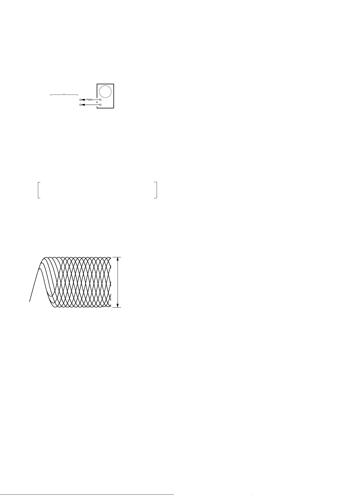
1. Open the upper lid.
2. Push the S401 as shown in Fig. 1.
3. Press the fl key
4. Check the object lens for confirming normal emission of the
laser diode. If not emitting, there is a trouble in the automatic
power control circuit or the optical pick-up.
During normal operation, the laser diode is turned ON about
2.5 seconds for focus searching.
S401
Fig. 1 Method to push the S401
– 16 –

• Method-2 (In service mode or normal operation):
Check the value of current flowing in the laser diode.
1. Remove the upper cabinet.
2. Read the current printed on the label attached on the rear side
of the optical pick-up.
(Label stuck outside of the
optical pick-up)
KSS-331C
24Y59
day
action number
year
month
SA350
Indicates current value.
(In this case, 35.0 mA)
A current value will vary depending on the set.
3. Connect a digital voltmeter as shown in Fig. 2.
4. Press the fl key.
5. Calculate current value by the reading of the digital voltmeter .
Reading of the digital voltmeter (V) ÷ 4.7 (Ω) = current value
(A) (Example) Reading of the digital voltmeter of 0.1645 V:
0.1645 V ÷ 4.7 Ω = 0.035 (A) = 35 mA
6. Check that the current value is within the following range.
• Current value of the label mA (25˚C)
Variation by temperature: 0.4 mA/˚C
Current increases with temperature increased.
Current decreases with temperature decreased.
If the current is more than the range above, there is a trouble
in the automatic power control circuit or the laser diode is in
deterioration.
If less than the range, a trouble exists in the automatic power
control circuit or the optical pick-up.
+5
–11
– MAIN Board – (Side B)
IC601
Q501
IC501
IC502
Fig. 2 Digital voltmeter connecting location
– 17 –
digital voltmeter
+
–

SECTION 3
DISASSEMBLY
Note: Follow the disassembly procedure in the numerical order given.
3-1. CABINET (UPPER) ASS’Y
2
two claws
2
claw
3
cabinet (upper) ass’y
2
claw
1
two screws
(2
1
three screws
×
8)
(2
×
8)
2
claw
– 18 –

3-2. UPPER LID BLOCK ASS’Y
d
y
1
spring (lock)
2
spring
(open)
5
4
Open the upper li
block ass’y.
shaft
3
Push the open button.
7
Pull up the upper lid block
ass’y to direction of arrow
A
B
.
8
Remove the upper lid block ass’
B
to direction of arrow C.
C
6
Close the upper lid block ass’y
to direction of arrow
A
.
– 19 –

SECTION 4
SERVICE MODE (TEST MODE)
• In this set, there are two test modes; CD-DA Test Mode and
VIDEO CD Test Mode.
4-1. How to Enter the Test Mode
1. Disconnect external power (no current is applied to the set).
2. Bridge the SOL701 (TEST) on the MAIN Board with a sol-
der. (IC701 (∞ (TEST) pin is shorted to the ground.)
3. Connect the external power.
4. The CD-DA Test Mode is activated. (LCD display v aries in 5-
ways, and its 5-way display is repeated.)
5. Before connecting external power in step 3, if π (POWER
OFF) key was pressed, the mode is switched to VIDEO CD
Test Mode.
(On the LCD, all segments are displayed, and the TV monitor
becomes 100% white.)
4-2. How to Release the Test Mode
1. Always disconnect external power , and break the solder bridge
of SOL701 (TEST) on the MAIN Board.
2. Thus, the set become ready for normal operation.
4-3. Each key Function in Test Mode
1. CD-DA Test Mode
Switches Description
π
(POWER OFF)
fl
(PLAY/PAUSE)
g Repeat once more the processing currently
SELECT selected with fl (PLAY/PAUSE) key.
±
(NEXT)
≠
(PREV)
ˆ
(RETURN)
ESP
REPEAT/
ENTER
+
MENU Raise K23** by one step after Tracking
–
MENU Lower K23** by one step after Tracking
* Coefficient of Focus Gain
** Coefficient of Tracking Gain
Stop processing
Press once: Initialize, Average Correct
Press twice: Auto Focus
Press 3 times: Focus Auto Gain
Press 4 times: Tracking Auto Gain
Press 5 times: All Servo ON, Mute OFF
Move optical pick-up toward outside track
Move optical pick-up toward inside track
Turn off the Mute
Turn on/off the ESP (f ast speed play, when
ON)
Tracking Gain up/normal switching
Raise K13* by one step after Focus Auto
Gain
Auto Gain
Lower K13* by one step after Focus Auto
Gain
Auto Gain
2. VIDEO CD Test Mode
Switches Description
π
(POWER OFF)
g
SELECT
– MAIN Board – (Side A)
TV monitor
Go to CD-DA Test Mode
Video system reset (return to 100% white
screen)
Monitor IN
Video OUT
J901
CN501
CN701
SOL701
(TEST)
Fig. 1 Test terminal location and connecting position
– 20 –

SECTION 5
A
B
0 V
A
B
0 V
1.2
±
0.5 Vp-p
A=B A=B
Note: Take long sweep time
for easy monitoring.
ELECTRICAL ADJUSTMENTS
5-1. Precautions for Adjustment
1. Before beginning adjustment, set the equipment to service
mode.
After the completion of adjustment, be sure to reset the service mode.
For more information, see “Service Mode (Test Mode)” on
page 20.
2. Perform adjustments in the order given.
3. Use YEDS-18 disc (Part No.: 3-702-101-01) unless otherwise
indi- cated.
4. Power supply voltage requirement: DC6 V
HOLD switch : OFF
VOLUME control : Minimum
RESUME switch : OFF
5-2. Before Beginning Adjustment
Set the equipment to service mode (See page 20) and check the
following. If there is an error, repair the equipment.
• Checking of the sled motor
1. Open the upper lid.
2. Press the fl key once.
3. Press the ± and ≠ keys and check that the optical pickup can move smoothly without sluggishness or abnormal noise
in innermost periphery → outermost periphery → innermost
periphery.
± : The optical pick-up moves outwardly.
≠ : The optical pick-up moves inwardly.
5-3. Tracking Balance Check
Condition:
• Hold the set in horizontal state.
Connection:
MAIN board
TP524 (TE)
TP534 (VC)
(see page 23)
oscilloscope
(DC range)
+
–
Checking Method:
1. Connect the oscilloscope to TP524 (TE) and TP534 (VC)
on the MAIN board.
2. Set the equipment to service mode stop state. (See page
20.)
3. Press the fl key once.
4. Move the optical pick-up to the center by pressing the ±
and ≠ keys.
5. Put the disc (YEDS-18).
6. Press the fl key twice.
From focus searching, focus is turned ON while entering CLV drawing-in mode. Tracking and sled are
turned OFF.
7. Confirm that a waveform on the oscilloscope is vertically
symmetric against 0 V.
• Checking of focus searching
1. Open the upper lid.
2. Press the fl key thrice. (Focus searching operation is activated continuously.)
3. Check the object lens of the optical pick-up for smooth up/
down motion without sluggishness or abnormal noise.
4. Press the π key.
Check that focus searching operation is deactivated. If not,
again press the π key slightly longer.
8. Stop removing of the disc motor by pressing the π key.
9. After the completion of check, reset service mode. (See
page 20.)
Connection Location: MAIN board (See page 23.)
– 21 –
5-4. Focus Bias Check
Condition:
• Hold the set in horizontal state.
Connection:
oscilloscope
(AC range)
MAIN board
TP535 (RFO)
TP534 (VC)
(see page 23)
2 k
Ω
+
–
Checking Method:
1. Connect the oscilloscope to TP535 (RFO) and TP534
(VC) on the MAIN board.
2. Set the equipment to service mode stop state. (See page
20.)
3. Press the fl key once.
4. Move the optical pick-up to the center by pressing the
± and ≠ keys.
5. Put the disc (YEDS-18).
6. Press the fl key four times.
From focus searching, focus is turned ON while entering CL V dra wing-in mode. Both tracking and sled
are turned ON.
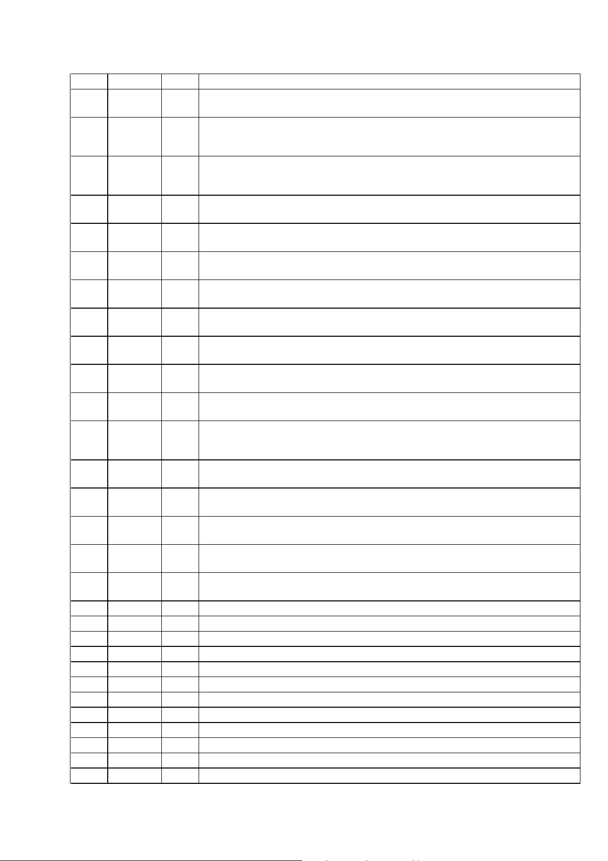
7. Check the oscilloscope waveform is as shown below.
A good eye pattern means that the diamond shape (≈) in
the center of the waveform can be clearly distinguished.
RF SIGNAL REFERENCE WAVEFORM (EYE PATTERN)
VOLT/DIV : 200 mV (With the 10:1 probe in use)
TIME/DIV: 500 ns
RF level
0.7 ± 0.2 Vp-p
To watch the eye pattern, set the oscilloscope to AC range
and increase the vertical sensitivity of the oscilloscope
for easy watching.
8. Stop revolving of the disc motor by pressing the π key.
9. After the completion of check, reset service mode. (See
page 20.)
Connection Location: MAIN board (See page 23.)
– 22 –

Connection Location
– MAIN Board – (Side A)
CN501
CN701
TP534
(VC)
TP524
(TE)
TP535
(RFO)
– 23 –
SECTION 6
DIAGRAMS
6-1. IC PIN FUNCTION DESCRIPTION
• MAIN BOARD (1/2) IC601 CXD2545Q
(DIGITAL SIGNAL PROCESSOR, FOCUS/TRACKING/SLED SERVO, EFM COMPARATOR)
Pin No. Pin Name I/O Function
1 SRON O Sled servo drive PWM signal output terminal Not used (open)
2 SRDR O
3 SFON O
4 TFDR O
5 TRON O
6 TRDR O
7 TFON O
8 FFDR O
9 FRON O
10 FRDR O Focus servo drive PWM signal (–) output to the MPC17A38ZVMEL (IC502)
11
12
13 VCOI I Oscillator circuit input terminal for analog PLL of the playback EFM
14 TEST I Input terminal for the test (fixed at “L”)
15 DVSS —
16 TES2 I Input terminal for the test (fixed at “L”)
17 TES3 I Input terminal for the test (fixed at “L”)
18 PDO O
19 VPCO O PLL charge-pump output terminal for the variable pitch Not used (open)
20 VCKI I Master clock signal (16.9344 MHz) input from the D/A converter (IC320) for the variable pitch
21
22
23
24
25
26
27 TE I
28 SE I Sled error signal input from the CXA1791N (IC501)
29
30
31
32
33
34
35
36
37
38
39
40 AVD1 — Power supply terminal (+3.3V) (analog system)
41 DVDD — Power supply terminal (+3.3V) (digital system)
42 ASYE I Playback EFM asymmetry circuit on/off selection input terminal (fixed at “H”)
43 PSSL I Audio data output mode selection input terminal (fixed at “L”)
44 WDCK O Word clock signal (88.2 kHz) output terminal Not used (open)
FFON O Focus servo drive PWM signal output terminal Not used (open)
VCOO O Oscillator circuit output terminal for analog PLL of the playback EFM
AVD2 — Power supply terminal (+3.3V) (analog system)
IGEN I Power supply terminal (+3.3V) (for operational amplifier)
AVS2 — Ground terminal (analog system)
ADIO I Input terminal for the A/D converter Not used (open)
RFC O Output terminal of the operational amplifier Not used (open)
RFDC I RF signal (DC level) input terminal for the digital servo process
FE I Focus error signal input from the CXA1791N (IC501)
VC I Middle point voltage (+1.65V) input from the CXA1791N (IC501)
FILO O Filter output terminal for master clock of the playback master PLL
FILI I Filter input terminal for master clock of the playback master PLL
PCO O Phase comparison output terminal for master clock of the playback EFM master PLL
CLTV I Internal VCO control voltage input of the playback master PLL
AVS1 — Ground terminal (analog system)
RFAC I RF signal (AC level) input terminal for the EFM demodulator
BIAS I Constant current input terminal of the playback EFM asymmetry circuit
ASYI I Playback EFM asymmetry comparator voltage input terminal
ASYO O
Sled servo drive PWM signal (–) output to the MPC17A38ZVMEL (IC502)
Sled servo drive PWM signal output terminal Not used (open)
Tracking servo drive PWM signal (–) output to the MPC17A38ZVMEL (IC502)
Tracking servo drive PWM signal output terminal Not used (open)
Tracking servo drive PWM signal (+) output to the MPC17A38ZVMEL (IC502)
Tracking servo drive PWM signal output terminal Not used (open)
Focus servo drive PWM signal (+) output to the MPC17A38ZVMEL (IC502)
Focus servo drive PWM signal output terminal Not used (open)
Ground terminal (digital system)
Charge-pump output terminal for analog PLL of the playback EFM Not used (open)
Tracking error signal input from the CXA1791N (IC501)
Playback EFM full-swing output terminal
– 24 –
Pin No. Pin Name I/O Function
45 LRCK O
L/R sampling clock signal (44.1 kHz) output to the D-RAM controller (IC680) and MPEG
46 DATA O
47 BCLK O
48 64 DATA O
49 64 BCLK O
50 64 LRCK O
51 GTOP O
52 XUGF O
53 XPLCK O
54 GFS O
55 RFCK O
56 C2PO O
57 XRAOF O
58 MNT3 O
59 MNT2 O
60 MNT1 O
61 MNT0 O
62 XTAI I Master clock signal (16.9344 MHz) input from the D/A converter (IC320)
63 XTAO O Master clock output terminal (16.9344 MHz) Not used (open)
64 XTSL I Master clock selection input terminal (fixed at “L”)
65 DVSS — Ground terminal (digital system)
66 FSTI I 2/3 divider input terminal of pins ^™ (XATI) and ^£ (XTAO)
67 FSTO O 2/3 divider output terminal of pins ^™ (XATI) and ^£ (XTAO)
68 C4M O 4.2336 MHz clock signal output terminal Not used (open)
69 C16M O 16.9344 MHz clock signal output terminal Not used (open)
70 MD2 I Digital out on/off control signal input terminal Fixed at “H” in this set
71 DOUT O Digital signal (for coaxial out and optical out) output terminal Not used (open)
72 EMPH O Emphasis control signal output terminal Not used (open)
73 WFCK O Write frame clock signal output terminal Not used (open)
audio/video decoder (IC901)
DA16 output when PSSL=“H”, 48-bit slot serial data output when PSSL=“L”
(PSSL (pin $£)=fixed at “L”) Serial data output to the D-RAM controller (IC680) and MPEG
audio/video decoder (IC901)
DA15 output when PSSL=“H”, 48-bit slot bit clock signal output when PSSL=“L”
(PSSL (pin $£)=fixed at “L”) Bit clock signal (2.8224 MHz) output to the D-RAM controller
(IC680) and MPEG audio/video decoder (IC901)
DA14 output when PSSL=“H”, 64-bit slot serial data output when PSSL=“L”
(PSSL (pin $£)=fixed at “L”) Not used (open)
DA13 output when PSSL=“H”, 64-bit slot bit clock signal output when PSSL=“L”
(PSSL (pin $£)=fixed at “L”) Not used (open)
DA12 output when PSSL=“H”, 64-bit slot L/R sampling clock signal output when PSSL=“L”
(PSSL (pin $£)=fixed at “L”) Not used (open)
DA11 output when PSSL=“H”, GTOP signal output when PSSL=“L”
(PSSL (pin $£)=fixed at “L”) Not used (open)
DA10 output when PSSL=“H”, XUGF signal output when PSSL=“L”
(PSSL (pin $£)=fixed at “L”) Not used (open)
DA09 output when PSSL=“H”, XPLCK signal output when PSSL=“L”
(PSSL (pin $£)=fixed at “L”) Not used (open)
DA08 output when PSSL=“H”, GFS (guard frame sync) signal output when PSSL=“L”
(PSSL (pin $£)=fixed at “L”) Not used (open)
DA07 output when PSSL=“H”, RFCK (read frame clock) signal output when PSSL=“L”
(PSSL (pin $£)=fixed at “L”) Read frame clock signal output to the D-RAM controller (IC680)
DA06 output when PSSL=“H”, C2PO signal output when PSSL=“L”
(PSSL (pin $£)=fixed at “L”) C2PO signal output to the D-RAM controller (IC680) and MPEG
audio/video decoder (IC901)
DA05 output when PSSL=“H”, XRAOF (RAM over flow) signal output when PSSL=“L”
(PSSL (pin $£)=fixed at “L”) Not used (open)
DA04 output when PSSL=“H”, MNT3 (monitor 3) signal output when PSSL=“L”
(PSSL (pin $£)=fixed at “L”) Not used (open)
DA03 output when PSSL=“H”, MNT2 (monitor 2) signal output when PSSL=“L”
(PSSL (pin $£)=fixed at “L”) Not used (open)
DA02 output when PSSL=“H”, MNT1 (monitor 1) signal output when PSSL=“L”
(PSSL (pin $£)=fixed at “L”) Not used (open)
DA01 output when PSSL=“H”, MNT0 (monitor 0) signal output when PSSL=“L”
(PSSL (pin $£)=fixed at “L”) Not used (open)
– 25 –
 Loading...