

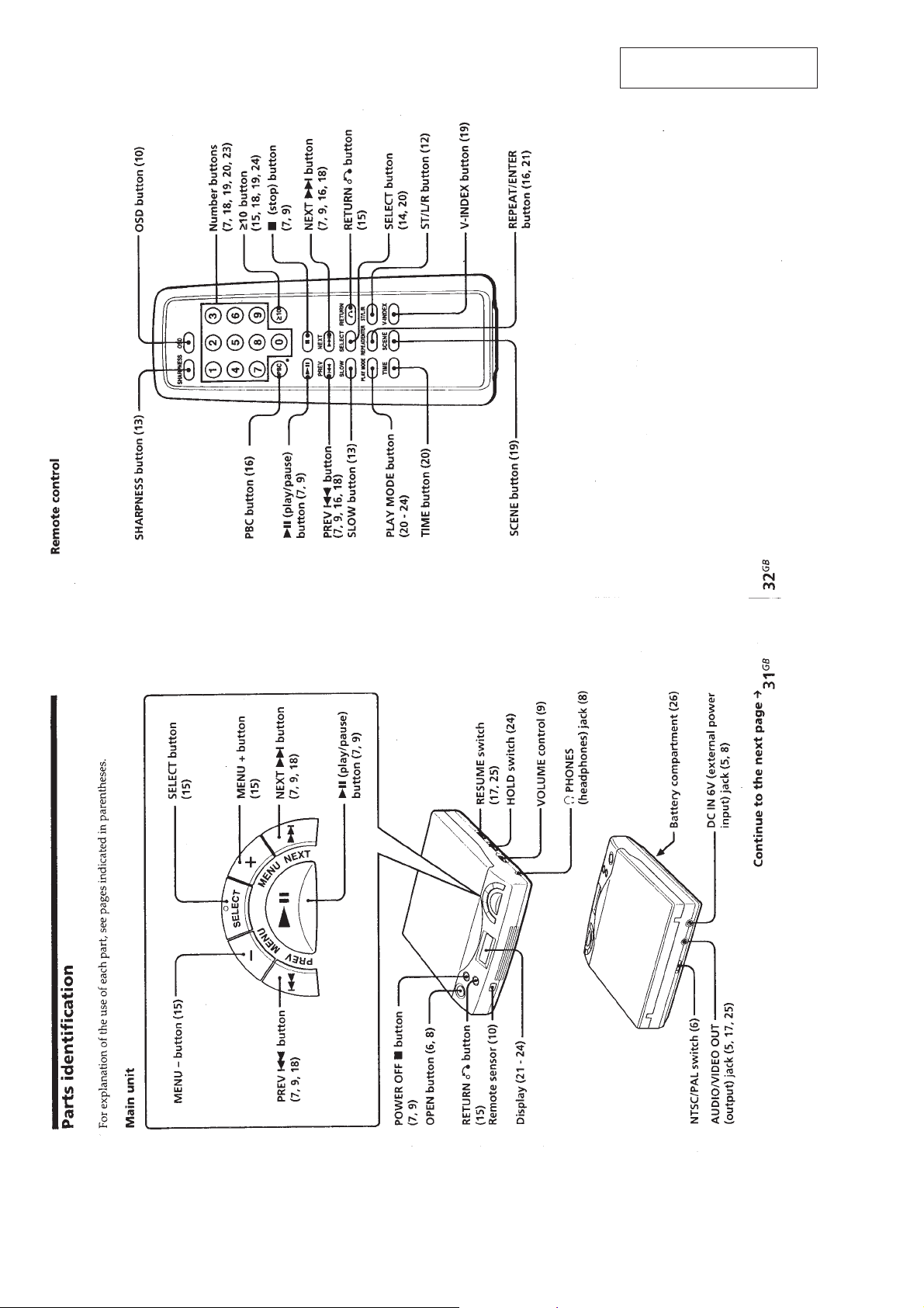
Page 1

D-V7000
SERVICE MANUAL
Ver 1.1 2000. 02
SPECIFICATIONS
E Model
Chinese Model
Model Name Using Similar Mechanism NEW
CD Mechanism Type CDM-2401AAA
Optical Pick-Up Name DAX-01A2
MICROFILM
PORTABLE VIDEO CD PLAYER
Page 2

TABLE OF CONTENTS
1. SERVICING NOTES ............................................... 3
2. GENERAL ................................................................... 4
3. DISASSEMBLY ......................................................... 5
4. SERVICE MODE (TEST MODE)..................... 7
5. ELECTRICAL ADJUSTMENTS......................... 8
Flexible Circuit Board Repairing
• Keep the temperature of the soldering iron around 270 ˚C during repairing.
• Do not touch the soldering iron on the same conductor of the
circuit board (within 3 times).
• Be careful not to apply force on the conductor when soldering
or unsoldering.
Notes on chip component replacement
• Never reuse a disconnected chip component.
• Notice that the minus side of a tantalum capacitor may be damaged by heat.
6. DIAGRAMS
6-1. Block Diagram ................................................................ 11
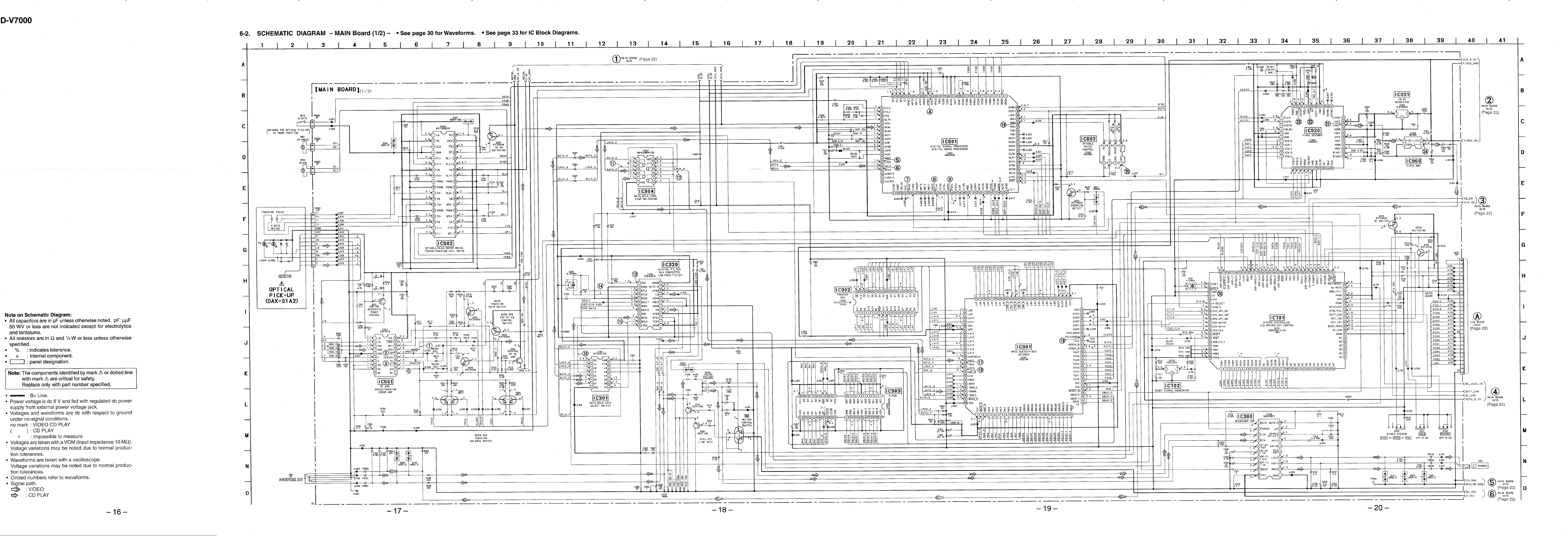
6-2. Schematic Diagram – MAIN Board (1/2) – ................... 17
6-3. Schematic Diagram – MAIN Board (2/2) – ................... 21
6-4. Printed Wiring Board – MAIN Board – ........................ 24
6-5. Printed Wiring Board – LCD Board –........................... 27
6-6. Schematic Diagram – LCD Board –.............................. 28
6-7. IC Pin Function Description ........................................... 38
7. EXPLODED VIEWS ................................................ 46
8. ELECTRICAL PARTS LIST ............................... 49
CAUTION
Use of controls or adjustments or performance of procedures
other than those specified herein may result in hazardous radiation exposure.
SAFETY-RELATED COMPONENT WARNING!!
COMPONENTS IDENTIFIED BY MARK ! OR DOTTED
LINE WITH MARK ! ON THE SCHEMA TIC DIAGRAMS
AND IN THE PARTS LIST ARE CRITICAL TO SAFE
OPERATION. REPLACE THESE COMPONENTS WITH
SONY PARTS WHOSE PART NUMBERS APPEAR AS
SHOWN IN THIS MANUAL OR IN SUPPLEMENTS PUBLISHED BY SONY.
– 2 –
Page 3
SECTION 1
current value
A: less than 48 mA
AC2211397
r
SERVICING NOTES
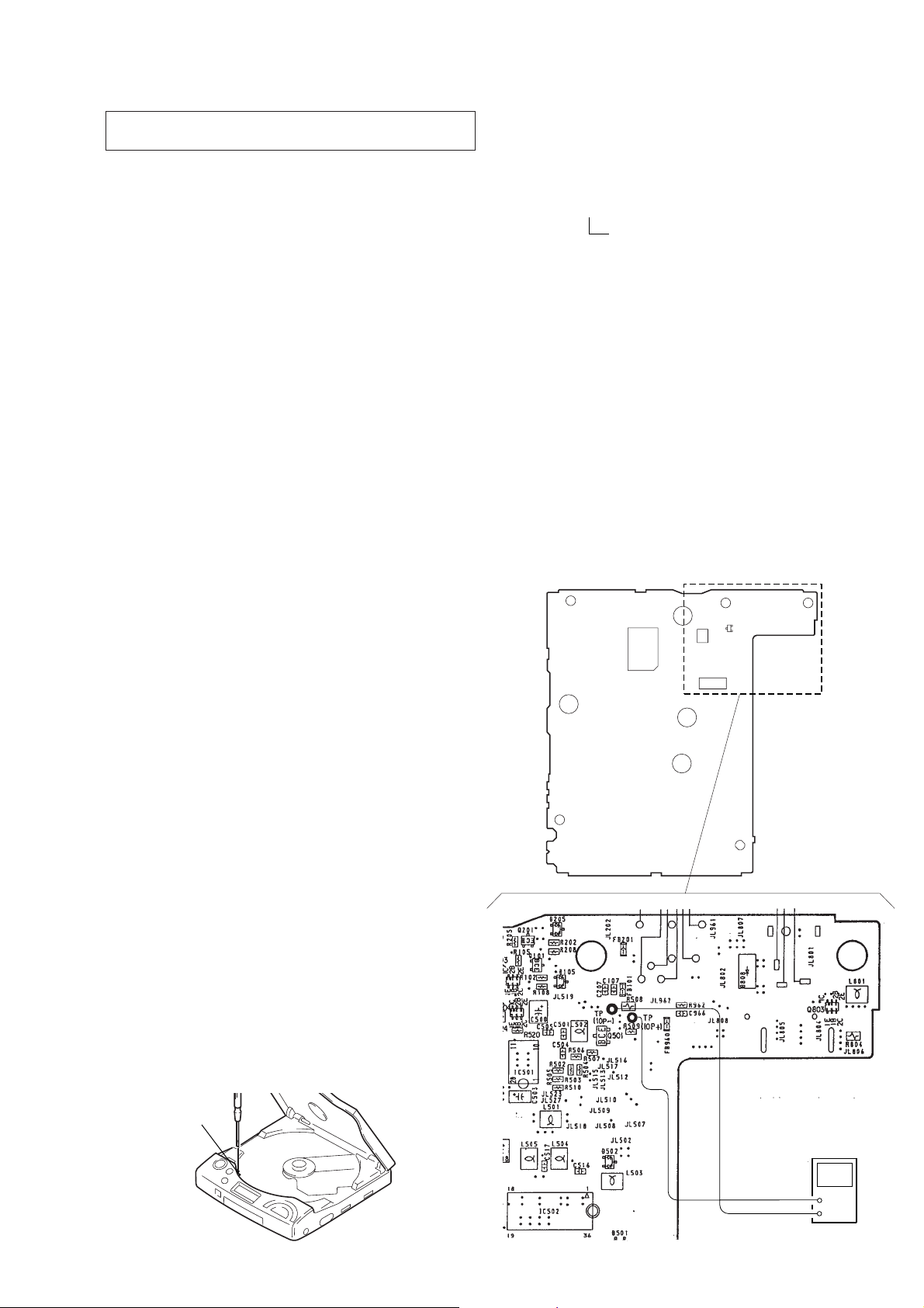
NOTES ON HANDLING THE OPTICAL PICK-UP
BLOCK OR BASE UNIT
The laser diode in the optical pick-up block may suffer electrostatic breakdown because of the potential difference generated by
the charged electrostatic load, etc. on clothing and the human body .
During repair, pay attention to electrostatic breakdown and also
use the procedure in the printed matter which is included in the
repair parts.
The flexible board is easily damaged and should be handled with
care.
NOTES ON LASER DIODE EMISSION CHECK
The laser beam on this model is concentrated so as to be focused
on the disc reflective surface by the objective lens in the optical
pick-up block. Therefore, when checking the laser diode emission, observe from more than 30 cm away from the objecti ve lens.
Before Replacing the Optical Pick-Up Block
Please be sure to check thoroughly the parameters as par the “Optical Pick-Up Block Checking Procedures” (Part No.: 9-960-027-
11) issued separately before replacing the optical pick-up block.
Note and specifications required to check are given below.
• FOK output: IC601 (£ pin (FOK)
When checking FOK, remove the lead wire to disc motor.
• S curve P-to-P value: 0.6-1.8 Vp-p IC501 !§ pin
When checking S curve P-to-P value, remove the lead wire to
disc motor.
• RF signal P-to-P value: 0.8-1.2 Vp-p
• Traverse signal P-to-P value: 1.2 Vp-p
• The repairing grating holder is impossible.
Precautions for Checking Emission of Laser Diode
Laser light of the equipment is focused by the object lens in the
optical pick-up so that the light focuses on the reflection surface
of the disc.
Therefore, be sure to keep your eyes more than 30 cm apart from
the object lens when you check the emission of laser diode.
• Method-2 (In the service mode or normal operation):
Check the value of current flowing in the laser diode.
1. Remove the upper cabinet.
2. Read the current printed on the rear side of the optical pick-
up. (Print on the rear side of the optical pick-up)
3. Connect a digital voltmeter as shown in Fig. 2.
4. Press the ^ key.
5. Calculate the current value by the r eading of the digital volt-
meter.
Reading of the digital voltmeter (V) ÷ 4.7 (Ω) = current value
(A) (Example) Reading of the digital voltmeter of 0.2256 V:
0.2256 V ÷ 4.7 Ω = 0.048 (A) = 48 mA
6. Check that the current value is within the following range.
• Current value of the label +5 mA (25˚C)
–11
Variation by temperature: 0.4 mA/˚C
Current increases with temperature increased.
Current decreases with temperature decreased.
If the current is more than the range above, there is a trouble
in the automatic power control circuit or the laser diode is in
deterioration.
If less than the range, a trouble exists in the automatic power
control circuit or the optical pick-up.
— MAIN Board — (Side B)
IC601
Q501
IC501
IC502
Laser Diode Checking Methods
During normal operation of the equipment, emission of the laser
diode is prohibited unless the upper lid is closed while turning ON
the S401 (push switch type).
The following two checking methods for the laser diode are operable.
• Method-1 (In the service mode or normal operation):
Emission of the laser diode is visually checked.
1. Open the upper lid.
2. Push the S401 as shown in Fig. 1.
3. Press the ^ key
4. Check the object lens for confirming normal emission of the
laser diode. If not emitting, there is a trouble in the automatic
power control circuit or the optical pick-up.
During normal operation, the laser diode is turned ON about
2.5 seconds for focus searching.
S401
TP (IOP +)
TP (IOP
digital voltmete
+
–
−
)
Fig. 1 Method to push the S401
– 3 –
Fig. 2 Digital voltmeter connecting location
Page 4
SECTION 2
GENERAL
This section is extracted from
instruction manual.
– 4 –
Page 5

SECTION 3
DISASSEMBLY
Note: Follow the disassembly procedure in the numerical order given.
3-1. CABINET (UPPER) ASSY
2
two claws
2
claw
3
cabinet (upper) assy
2
claw
1
two screws
(2
1
three screws
×
8)
(2
×
8)
2
claw
– 5 –
Page 6

3-2. LID BLOCK ASSY, UPPER
”
1
spring (lock)
2
spring
(open)
5
shaft
4
Open the “lid block assy, upper”.
3
Push the open button.
7
Pull up the “lid block assy, upper”
to direction of arrow
A
B
.
B
8
Remove the “lid block assy, upper
to direction of arrow C.
C
6
Close the “lid block assy, upper”
to direction of arrow
A
.
– 6 –
Page 7
SECTION 4
SERVICE MODE (TEST MODE)
• In this set, there are two test modes; CD-DA Test Mode and
VIDEO CD Test Mode.
How to Enter the Test Mode
1. Disconnect exter nal power (no current is applied to the set).
2. Bridge the SOL701 (TEST) on the MAIN Board with a sol-
der. (IC701 (∞ (TEST) pin is shorted to the ground)
3. Connect the external power.
4. The CD-DA Test Mode is activ ated. (LCD display v aries in 5-
ways, and its 5-way display is repeated)
5. Before connecting exter nal power in step 3, if p (POWER
OFF) key was pressed, the mode is switched to VIDEO CD
Test Mode.
(On the LCD, all segments are displayed, and the TV monitor
becomes 100% white)
How to Release the Test Mode
1. Alw ays disconnect external power , and break the solder bridge
of SOL701 (TEST) on the MAIN Board.
2. Thus, the set become ready for normal operation.
Each key Function in Test Mode
1. CD-DA Test Mode
Switches Description
p
(POWER OFF)
^
(PLAY/PAUSE)
g Repeat once more the processing currently
SELECT selected with ^ (PLAY/PAUSE) key.
+
(NEXT)
=
(PREV)
ˆ
(RETURN)
+
MENU Raise K23** by one step after Tracking
–
MENU Lower K23** by one step after Tracking
* Coefficient of Focus Gain
** Coefficient of Tracking Gain
Stop processing
Press once: Initialize, Average Correct
Press twice: Auto Focus
Press 3 times: Focus Auto Gain
Press 4 times: Tracking Auto Gain
Press 5 times: All Servo ON, Mute OFF
Move optical pick-up toward outside track
Move optical pick-up toward inside track
Turn off the Mute
Raise K13* by one step after Focus Auto
Gain
Auto Gain
Lower K13* by one step after Focus Auto
Gain
Auto Gain
2. VIDEO CD Test Mode
Switches Description
p
(POWER OFF)
g Video system reset (return to 100% white
SELECT screen)
– MAIN Board – (Side A)
TV monitor
Go to CD-DA Test Mode
Monitor IN
Video OUT
J901
CN501
CN701
SOL701
(TEST)
Fig. 1 Test terminal location and connecting position
– 7 –
Page 8

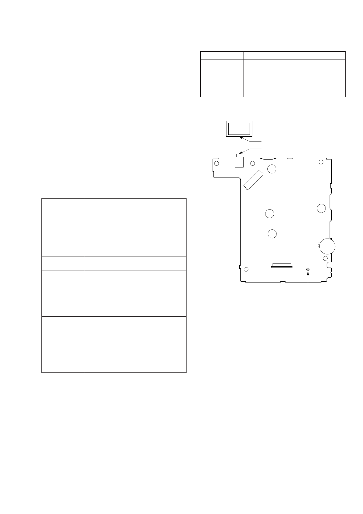
SECTION 5
MAIN board
TP524 (TE)
TP534 (VC)
(see page 10)
+
–
oscilloscope
(DC range)
2200 pF
10 k
Ω
A
ELECTRICAL ADJUSTMENTS
Precautions for Adjustment
1. Before beginning adjustment, set the equipment to service
mode.
After the completion of adjustment, be sure to reset the service mode.
For more information, see “Service Mode (Test Mode)” on
page 7.
2. Perform adjustments in the order given.
3. Use YEDS-18 disc (Part No.: 3-702-101-01) unless otherwise
indicated.
4. Power supply voltage requirement: DC6 V
HOLD switch : OFF
VOLUME control : Minimum
RESUME switch : OFF
Before Beginning Adjustment
Set the equipment to service mode (See page 7) and check the
following. If there is an error, repair the equipment.
• Checking of the sled motor
1. Open the upper lid.
2. Press the ^ key once.
3. Press the + and = keys and check that the optical pickup can move smoothly without sluggishness or abnormal noise
in innermost periphery → outermost periphery → innermost
periphery.
+ : The optical pick-up moves outwardly.
= : The optical pick-up moves inwardly.
• Checking of focus searching
1. Open the upper lid.
2. Press the ^ key thrice. (Focus searching operation is activated continuously.)
3. Check the object lens of the optical pick-up for smooth up/
down motion without sluggishness or abnormal noise.
4. Press the p key.
Check that focus searching operation is deactivated. If not,
again press the p key slightly longer.
Tracking Balance Check
Condition:
• Hold the set in horizontal state.
Connection:
Checking Method:
1. Connect the oscilloscope to TP524 (TE) and TP534 (VC)
on the MAIN board.
2. Set the equipment to service mode stop state. (See page 7)
3. Move the optical pick-up to the center by pressing the +
and = keys.
4. Put the disc (YEDS-18).
5. Press the ^ key.
From focus searching, focus is turned ON while entering CLV drawing-in mode. Tracking and sled are
turned OFF.
6. Confirm that a waveform on the oscilloscope is vertically
symmetric against 0 V.
Note: Take long sweep time
for easy monitoring.
A
0 V
0.7 – 1.1 Vp-p
B
A=B A=B
0 V
7. Stop removing of the disc motor by pressing the p key.
8. After the completion of check, reset service mode. (See
page 7)
B
Connection Location: MAIN board (See page 10)
– 8 –
Page 9

Focus Bias Check
Condition:
• Hold the set in horizontal state.
Connection:
oscilloscope
(AC range)
MAIN board
TP535 (RFO)
TP534 (VC)
(see page 10)
+
–
Checking Method:
1. Connect the oscilloscope to TP535 (RFO) and TP534
(VC) on the MAIN board.
2. Set the equipment to service mode stop state. (See page
7)
3. Press the ^ key once.
4. Move the optical pick-up to the center by pressing the
+ and = keys.
5. Put the disc (YEDS-18).
6. Press the ^ key four times.
From focus searching, focus is turned ON while entering CL V drawing-in mode. Both tracking and sled
are turned ON.
7. Check the oscilloscope waveform is as shown below.
A good eye pattern means that the diamond shape (≈) in
the center of the waveform can be clearly distinguished.
RF SIGNAL REFERENCE WAVEFORM (EYE PATTERN)
VOLT/DIV: 200 mV (With the 10:1 probe in use)
TIME/DIV: 500 ns
RF level
0.7 – 1.1 Vp-p
T o watch the ey e pattern, set the oscilloscope to AC range
and increase the vertical sensitivity of the oscilloscope
for easy watching.
8. Stop revolving of the disc motor by pressing the p key.
9. After the completion of check, reset service mode. (See
page 7)
Connection Location: MAIN board (See page 10)
– 9 –
Page 10
Connection Location
– MAIN Board – (Side A)
CN501
CN701
TP534
(VC)
TP524
(TE)
TP535
(RFO)
– 10 –
Page 11

6-1. BLOCK DIAGRAM
RF 3.3V
A
BC
F
E
DETECTOR
OPTICAL PICK-UP
(DAX-01A2)
LASER DIODE
AUTOMATIC
POWER CONTROL
PD
LD
SPO+
M901
(SPINDLE)
M902
(SLED)
2-AXIS
DEVICE
(FOCUS)
05
(TRACKING)
TRK+
TRK–
FCS+
FCS–
22
M
M
SPO–
24
SLO+
29
SLO–
26
TO+
13
TO–
15
FO+
8
FO–
11
FOCUS/TRACKING ERROR AMP
PD1
3
4
6
7
Q501
SPINDLE
MOTOR DRIVE
SPINDLE/SLED MOTOR DRIVE,
FOCUS/TRACKING COIL DRIVE
IC502
SLED
MOTOR DRIVE
TRACKING
COIL DRIVE
FOCUS
COIL DRIVE
OE
33
CD ON
SWITCHING
Q507
RF
I-V
PD2
AMP
F
F I-V AMP
E
E I-V AMP
13 12
LD
1
SPI
SLI+
SLI–
TI+
TI–
ON :
When the optical pick-up
is inner position.
RF AMP,
IC501
EO
EI
TRACKING
BALANCE SWITCH
Q503, 504
TRV0
TRV1
TRV2
APC LD
AMP
F/R
20
19
31
32
17
18
FI+
6
FI–
5
S910
(LIMIT)
SECTION 6
DIAGRAMS
RF
RFO
SUMMING
AMP
FOCUS
ERROR AMP
FE BIAS
15
TRACKING
ERROR AMP
TRV3
APC PD
AMP
DIGITAL SERVO PROCESSOR
100
2
4
6
8
10
99
17
RFI
18
FE
16
TE
14
LDON
19
PD
2
SPINDLE MOTOR CONTROL
IC602
BUFFER
OUT
1
IC601 (2/2)
SFDR
SRDR
TFDR
TRDR
FFDR
FRDR
SSTP
PWM GENERATOR
FOCUS/TRACKING/SLED
SERVO MICRO
PROGRAM
INTERFACE
ESP RF EQ
CONTROL
SWITCH
Q508, 509
TE
TRACKING
GAIN SWITCH
Q505
COMPARATOR
SERVO DSP
FOCUS/TRACKING/SLED
RF DC AMP
Q506
FE
RF DC
MDS
COUT
89
MDP
5
SW
MIRR, DFCT,
FOK DETECTOR
SERVO AUTO
SEQUENCER
CPU
INTERFACE
DIGITAL SIGNAL PROCESSOR
IC601 (1/2)
RFAC
36
ASYMMETRY
CORRECTOR
ASYI
38
ASYO
39
OVERSAMPLING
NOISE
SHAPER
PROCESSOR
FSW
94
CONT
2
RFDC
26
FE
29
TE
A/D
CONVERTER
FOK
MIRR
DFCT
SENS
DATA
CLOK
XLAT
27
SE
28
93
91
92
80
86
88
87
MIX
18-TIMES
FILTER
CLV
MON
95 96 97
TRV0
TRV1
TRV2
TRV3
MDP
MDS
FILTER
34
31
33
PCO
FILO
DIGITAL PLL
VARI-PITCH
DOUBLE SPEED
SYNC
PROTECTOR
TIMING
GENERATOR 1
DSP-SCOR
ESP-POWER
58
59
TRVCTL
TRV0
63
TRV1
62
TRV2
61
TRV3
60
XLASERCTL
79
DSP-SENS
69 68 70 54 55 57
32
FILI
CLTV
EFM
DEMODULATOR
TIMING
GENERATOR 2
SUBCODE Q
PROCESSOR
SCOR
WFCK
748073 78 77 76 75
DSP-SBQCLK
DSP-SUBQ
DSP-SNSCLK
XAU-RESET
ESS-DATAO
ESS-DATAI
ESS-CLK
SYS XMT RQ
SYS RCV RDY
MPG XMT RQ
DSP-DATA
XDSPLT
XDACLT
DSP-CLK
SQCK
66
65
71
50
91
92
93
88
89
90
XLAT
DATA
CLK
REGISTER
32K
RAM
ADDRESS
GENERATOR
SUBQ
DATAO
DATAI
CLK
CTL0
CTL1
CTL2
PRIORITY
ENCODER
SUBCODE P – W
PROCESSOR
EXCK
SBSO
DATA
BCLK
LRCK
C16M
AU-POWER
CLOCK
GENERATOR
D/A DIGITAL
CORRECTOR
PEAK
6
3
11
8
OFF
ON
HOLD c
PROCESSOR
MUTE
TDMDR
97
TDMCLK
96
98
TDMFS
AUDIOCLK
88
46
AUX1
AUX2
47
66
LCS1 B
AUX7
54
AUX5
53
AUX6
52
HOLD
52
S701
DIGITAL
OUT
SCLK
SWITCHING
IC904
4
1/4
5
1
2/4
2
12
3/4
13
9
4/4
10
ERROR
DETECTOR
DATAO
DATAI
CLK
CTL0
CTL1
CTL2
INTERNAL BUS
EMPH
72 83 79 81
DATA, BCLK, LRCK, C16M
XTAI
VCKI
DATA
BCLK
LRCK
GFS
RFCK
PROCESSOR
C2PO
SERIAL/PARALLEL
DOUT
XRST
RESUME
53
OFF
ON
S702
RESUME
62
20
46
47
45
54
55
BCLK
DATA
56
71
LRCK
C16M
13 – 28 55 – 62
2 – 5, 7 – 10, 31 – 34, 36 – 39
DQ0 – DQ15
S703
(VIDEO SYSTEM)
D-RAM
IC903
NTSC/PAL
43
NTSC
AUTO
MA0 – MA8DBUS0 – DBUS15
16 – 19, 22 – 26
PAL
DATA
BCLK
LRCK
4 – 12
A0 – A8
DATA, BCLK, LRCK
SELECT SWITCH
IC301
IC301
2A
5 7 22
6
11
10
2
3
MPEG AUDIO/VIDEO
DECODER
IC901
29WE13OE27
KEY IN1, KEY IN2
S421, 422,
S441 – 446
2B
3A
3B
1A
1B
99
28
LCAS
40, 41
SEL
1
DCAS B
DRAS B2DWE B3DOE B
14
RAS
UCAS
2Y
3Y
9 23
1Y
4
92
CKO
13
DATA
BCLK
LRCK
24
LD0 – LD7
21 – 23, 25 – 29
O0 – O7
DOOR OPEN
39
SWITCHING
16 15
XTLO
OSC & TIMING
GENERATOR
INPUT
INTERFACE
CIRCUIT
MUTE-O
11
D340
LA0 – LA16
68 – 79, 82 – 86
20 – 13, 3, 2, 31, 1,
12, 4, 5, 11, 10
PROGRAM ROM
IC902
SYSTEM CONTROLLER,
LCD DRIVER, KEY CONTROL
IC701
Q702
SOL702
(DOOR)
(ON: When the CD lid is closed.)
X320
16.9344MHz
XTLI
DIGITAL
FILTER
CIRCUIT
A0 – A16
S401
OPEN
CPU
INTERFACE
SDATA
SHCK
20 19 18
CLK
DATA
S401
∆Σ
MODULATOR
CIRCUIT
DACLT
XLAT
LOE B64LCS3 B
65
32CE30
OE
TEST
95
DIGITAL FILTER,
D/A CONVERTER,
LOW-PASS FILTER
SOL701
(TEST MODE)
LOW-PASS
FILTER
LOW-PASS
FILTER
IC320
RESET B
29
51
XV-RESET
LO
9
RO
5
LINE MUTE
Q101, 201
CONTROL SWITCH
89
AOUT
TBCK
90
ATFS
91
YUV0 – YUV7
HSSCN B
41
40
VSSCN B
AUX3
48
PCLK2XSCN
43
COM1 – COM4
1 – 4
LIQUID CRYSTAL DISPLAY
MUTING
Q340
32 – 39
LCD401
VIDEO
DATA
SEG0 – SEG12
5 – 11, 13 – 18
∑ VOLUME
DATA
BCLK
LRCK
7 – 14
MIFH
1
MIFFL
2
MODE
15
RV301
-1
-2
COLOR BAR
GENERATOR
YDI0 – YCDI7
SEPARATOR
GENERATOR
Y/C
SYNC
CIRCUIT
TMS1
HEADPHONE AMP
LIN
13
RIN
14
MUTE
11
TMS0
44
SOL921
(COLOR BAR)
IC360
PWRSW
12
LOUT
ROUT
REF
BEEP
19
VIDEO ENCODER
Y LEVEL
ALIGNMENT
C LEVEL
ALIGNMENT
OSC1
82
X701
4.19MHz
4
2
3
IC920
VCD 3.3V
OSC0
C SYNC
ADD
C SIGNAL
GENERATOR
ROM
2 PHONES
AUDIO/VIDEO OUT
+
CK27O
42 38 3943
J301
J901
OSC
CIRCUIT
CK27I
X920
27MHz
RESET SIGNAL
GENERATOR
DAC
DAC
DAC
XO
RESET
9481
IC702
VCPU 3.3V
OUT
YOUT
COUT
D-V7000
• SIGNAL PATH
: CD PLAY
: VIDEO
VCPU 3.3V
+3.2V
VIDEO ENCODER
(IC920) B+
COMPARATOR
OSC
B+ SWITCH
Q882
SWITCHING
REGULATOR
Q881
SWITCHING
REGULATOR
Q822
COMPARATOR
COMPARATOR
OSC
D890
PWM
PWM
PWM
VCD 5V
IN
ERROR
4
AMP
Q810-2
VCD 3.3V
CV
VIDEO AMP
31
IC960
27
29
86
49
A-SELECT
AU-MUTE
REMOTE
CONTROL
RECEIVER
IC401
73
67
BEEP
V-POWER56DCINJACK44DC CHK
38
VCC
REMOTE
XIRCTL
B+ SWITCH
87
VIDEO CD ON
CD ON
Q703
VCPU 3.3V
ACD 3.3V,
RF 3.3V
MOTOR 2.8V
IN2
ERROR
3
AMP
IN1
ERROR
14
AMP
+3.2V
REGULATOR
IC801
+3.2V
REGULATOR
IC921
DC/DC
CONVERTER
Q891, T891
OUTPUT
CIRCUIT
POWER CONTROL
IC820
Q810-1
OUTPUT
CIRCUIT
OUTPUT
CIRCUIT
POWER CONTROL
IC861
DC/DC CONVERTER
CONTROL SWITCH
IC862 (1/2)
4
OUT
1
2
VCC
VOLTAGE
DETECT
IC810
SWITCHING REGULATOR
CONTROL SWITCH
15
14
OUT2
7
OUT1
10
9
VDD
H VCC
9
B+ SWITCH
IC862 (2/2)
11
10
B+ SWITCH
B+ SWITCH
Q801, 802
Q820
Q861
5
3
VCD 5V
DRY BATTERY
1
2
13
12
DC VOLTAGE
DETECT
Q803-2
DC IN
DETECT
Q803-1
D805
SIZE “AA”
(IEC DESIGNATION R6)
4PCS. 6V
J801
DC IN 6V
+
–
– 11 –
– 12 –
– 13 –
– 14 –
– 15 –
Page 12
Page 13

Page 14

Page 15

Page 16

• Wavef orms
12.8 Vp-p
5.2 µs
5.8 Vp-p
4.5 µs
– MAIN Board (1/2) –
1 IC501 !¶ (RFO)
200 mV/DIV, 500 ns/DIV
6 IC601 $¶ (BCLK)
1 V/DIV, 200 ns/DIV
!¡ IC904 3
2 V/DIV, 200 ns/DIV
!§ IC320 @¢ (LRCK)
1 V/DIV, 10 µs/DIV
@¡ IC920 #¡ (CVOUT)
500 mV/DIV, 20 µs/DIV
– MAIN Board (2/2) –
@§ IC820 1 (OUT)
2 V/DIV, 2 µs/DIV
#¡ T891 4
5 V/DIV, 2 µs/DIV
2 IC501 !§ (FE)
50 mV/DIV, 5 ms/DIV
3 IC501 !¢ (TE)
200 mV/DIV, 5 ms/DIV
0.9 ± 0.2 Vp-p
Approx.
50 mVp-p
Approx.
570 mVp-p
472 ns
7 IC601 %∞ (RFCK)
1 V/DIV, 50 µs/DIV
136 µs
8 IC601 ^™ (XTAI)
1 V/DIV, 20 ns/DIV
3.1 Vp-p
3.2 Vp-p
2.3 Vp-p
472 ns
!™ IC904 !¡
2 V/DIV, 5 µs/DIV
!£ IC320 !£ (CKO)
2 V/DIV, 20 ns/DIV
22.7 µs
4.1 Vp-p
3.3 Vp-p
0.84 Vp-p
22.7 µs
!¶ IC901 (º (TBCK)
1 V/DIV, 200 ns/DIV
472 ns
!• IC901 (¡ (ATFS)
1 V/DIV, 10 µs/DIV
3.3 Vp-p
3.2 Vp-p
3.2 Vp-p
H
@™ IC920 #ª (XO)
2 V/DIV, 20 ns/DIV
27 MHz
@£ IC920 $™ (CK270)
2 V/DIV, 20 ns/DIV
1.0 Vp-p
4.2 Vp-p
3.9 Vp-p
5.24 µs
@¶ IC861 1 (CT)
200 mV/DIV, 2 µs/DIV
µ
s
4.9
@• IC861 7 (OUT1)
2 V/DIV, 2 µs/DIV
5.27 Vp-p
680 mVp-p
5.5 Vp-p
#™ Q881 G
2 V/DIV, 2 µs/DIV
4.5
#£ Q881 D
2 V/DIV, 2 µs/DIV
5.4 Vp-p
µ
s
4 IC601 @º (VCKI)
1 V/DIV, 20 ns/DIV
16.9344 MHz
5 IC601 $∞ (LRCK)
1 V/DIV, 10 µs/DIV
22.7 µs
2.5 Vp-p
3.2 Vp-p
16.9344 MHz
9 IC601 ^§ (FSTI)
2 V/DIV, 50 ns/DIV
87 ns
0 IC601 (§ (MDP)
2 V/DIV, 2 µs/DIV
7.6 µs
3.8 Vp-p
3.7 Vp-p
59 ns
!¢ IC320 !§ (XTLO)
2 V/DIV, 20 ns/DIV
16.9344 MHz
!∞ IC320 @£ (BCLK)
2 V/DIV, 200 ns/DIV
472 ns
3.7 Vp-p
3.3 Vp-p
22.7 µs
!ª IC901 $£ (PCLK2XSCN)
2 V/DIV, 1 ms/DIV
27 MHz
@º IC701 *™ (OSC0)
1 V/DIV, 100 ns/DIV
4.19 MHz
5.2 Vp-p
2.72 Vp-p
27 MHz
@¢ IC960 1 (OUT)
500 mV/DIV, 20 µs/DIV
H
@∞ IC602 1 (OUT)
1 V/DIV, 2 µs/DIV
7.5
µ
s
2.0 Vp-p
3.1 Vp-p
4.6 µs
@ª IC861 0 (OUT2)
2 V/DIV, 2 µs/DIV
4.5 µs
#º Q891 G
2 V/DIV, 2 µs/DIV
5.2
µ
s
5.5 Vp-p
5.6 Vp-p
– 30 –
– 31 –
– 32 –
Page 17

• IC Block Diagrams
– MAIN Board (1/2) –
IC301 TC74VHC157F
IC320 TC9434AFNEL
INPUT
OUTPUT
INPUT
OUTPUT
SELECT
GND
111
2
1A
1A
3
1B
1B
4
1Y
1Y
5
2A
2A
6
2B
2B
7
2Y
2Y
8
16
V
S
3Y
CC
15
STROBE
G
4A
14
4A
4B
4Y
3A
3B
INPUT
4B
13
12
11
4Y
OUTPUT
3A
11
INPUT
3B
10
3Y
OUTPUT
9
TEST
CIRCUIT
VDD
INPUT INTERFACE
21 3
T1
LRCK
BCK
DATA
CIRCUIT
DIGITAL FILTER CIRCUIT,
DIGITAL BASS BOOST CIRCUIT,
ATTENUATOR OPERATIONAL CIRCUIT,
DE-EMPHASIS FILTER CIRCUIT
∆Σ MODULATOR CIRCUIT
OUTPUT
CIRCUIT
ANALOG
FILTER
5 6 7 9 10
4
VDA
RO
P/S
ATT (LB1)
LB2
GNDAVRGNDA
SH (EMP)
20 16 15
CPU INTERFACE
CIRCUIT
OUTPUT
CIRCUIT
ANALOG
FILTER
8
LA (SM)
LO
VDX
17212224 23
TIMING GENERATOR
VDA
XO
XI
14
OSCILLATOR
11
12
ZD
GNDX
1319 18
GNDD
MCKO
IC360 BA3574BFS
11
MUTE SW
12
IN 1
IN 2
P.SW
13
14
15
16
17
RIPPLE
FILTER
18
19
20
V
CC
PW SW
BIAS OUT
BIAS IN
RF OUT
RF IN
BEEP IN
BEEP
MUTE
BB SW
AVC DET
10
9
8
7
6
5
4
3
2
1
MUTE
LP
MUTE SW
AVC
AVC IN
MIX OUT
OUT 1
VREF
OUT 2
GND
– 33 –
Page 18

IC501 CXA1791N
1
LD
APC
PD AMP
+
–
–
+
VC
RF
IV AMP1
–
+
VC
RF
IV AMP2
–
+
VC
VC
VC
F
IV AMP
–
+
E
IV AMP
PD1
PD2
GND
2
PD
3
4
5
6
F
7
E
8
VR
9
VC
10
NC
VREF
1.25V
APC
LD AMP
+
–
VC
VC
VC BUFFER
VC
VCC
–
+
VC
SUMMING AMP
–
+
FOCUS
ERROR AMP
VC
VC
–
VC
+
–
+
VCC
TRACKING
ERROR AMP
20
VCC
19
APC ON
18
RFI
17
16
15
14
13
12
11
RFO
FE
FE BIAS
TE
EI
EO
NC
RF
IC502 MPC17A38ZVMEL
VG
GNDPSOE
36 35 34 33 32 31 30 29 28 27 26 25 24 23 22 21 20 19
DC/DC
CONVERTER
VC
CLOCK
VC VC
CLK
DETECTOR
VC
2 3
1
LG
5 6 7 8 9 10 14
4
VC
CLK
GND
RI1
VD
FI1
FO1
PGND
FI3
RI3
DRIVER
PRE-DRIVER
CONTROL
PGND
PGND
PGND
FO3
VD
DRIVER
PRE-DRIVER
VC
CONTROL
RO1
VCVC
VD
RO2
PGND
VC
15131211
VD
FI2
FO2
RO3VDRO4
DRIVER
PRE-DRIVER
CONTROL
181716
RI2
VC
VC
PGND
FO4VDF/R4
DRIVER
PRE-DRIVER
CONTROL
PI4
– 34 –
Page 19

IC601 CXD2545Q
SBSO
EXCK
SQSO
SQCK
MUTE
SENS
XRST
DIRC
SCLK
DFSW
ATSK
DATA
XLAT
CLOK
COUT
ADD
MIRR
DFCT
FOK
FSW
MON
MDP
MDS
LOCK
SSTP
76
77
78
79
80
81
82
83
84
85
86
87
88
89
90
91
92
93
94
95
96
97
98
99
P-W
SUBCODE
PROCESSOR
Q
SUBCODE
PROCESSOR
CPU
CPU
INTERFACE
INTERFACE
AUTO
SERVO
SEQUENCER
SERVO
SCOR
WFCK
EMPH
TIMING
GENERATOR 1
32K RAM
INTERFACE
MICRO PROGRAM
CPU
ADDRESS
CLV
PROCESSOR
SYNC
PROTECTOR
D/A
DIGITAL
CPU
PRIORITY
INTERFACE
GENERATOR
NOISE
SHAPER
PROCESSOR
ENCODER
INTERFACE
FILTER
18-TIMES
OVER SAMPLING
D OUT
MD2
OUT
DIGITAL
PEAK
DETECTOR
RESISTER
CPU
ERROR
INTERFACE
CORRECTOR
FSTO
C16M
C4M
CPU
TIMING
INTERFACE
GENERATOR 2
3
DVSS
FSTI
CLOCK
GENERATOR
XTAI
XTAO
XTSL
6263646566676869707172737475
EFM
CPU
INTERFACE
DEMODULATOR
PLL
DIGITAL
VARI-PITCH
DA01|DA11
61 – 51
SERIAL
PARALLEL
MUX
CPU
ASYMMETRY
DOUBLE SPEED
46
|
50
45
44
43
PROCESSOR
42
41
40
39
38
INTERFACE
37
CORRECTION
36
35
34
33
32
31
DA16
|
DA12
LRCK
WDCK
PSSL
ASYE
ADD
AVDD
ASYO
ASYI
BIAS
RFAC
AVSS
CLTV
PCO
FILI
FILO
SFDR
SLED
SERVO
TRACKING
SLED PWM
GENERATOR
TRACKING PWM
100
2 345 6 7 8 9 10 11 201918171615141312
1
TFDR
SFON
SRDR
TRON
SRON
SERVO
GENERATOR
FFDR
TFON
TRDR
FOCUS
SERVO
GENERATOR
FOCUS PWM
FFON
FRON
FRDR
SERVO DSP
PWM GENERATOR
VCO0
VCO1
TEST
MIRR
DVSS
DFCT
TES2
FOK DETECTOR
PDO
TES3
VPCO
VCKI
4
A/D
SWITCH
CONVERTER
21 22 23 24 25
IGEN
ADIO
AVSS
AVDD
&
BUFFER
RFC
VC
30
FE
29
SE
28
TE
27
26
RFDC
– 35 –
Page 20

IC602 BA3890F
1OUT
2CONT
3CT
4GND
0.25V
BUFFBUFF
+
COMP
–
IC920 TC90A07U
33
HSYNC
34
VSYNC
35
TMS3
VDD
CK27I
GND
TMS2
CK27O
TMS1
TMS0
36
37
38
XO
39
40
41
42
43
44
SYNC
GENERATOR
CSYNC
8
7
6
5
AVCC
GENERATOR
CVOUT
3132
ALIGNMENT
DAC
CY
+
C SIGNAL
AGND
C LEVEL
INTERPOLATE
+
INTERPOLATE
ROM
21 3 54 6
MIFH
MIFFL
MIFFR
VBLNKI
Vcc
IN
2
V
IN
1
V
SW
COUT
AVCC
YOUT
28 23
DAC
DAC
C SYNC
ADD
BURST FLAG
BLANKING
Cb LEVEL
ALIGNMENT
VDD
GND
AGND
Y LEVEL
ALIGNMENT
LOW-PASS
FILTER
LOW-PASS
FILTER
VREF
2425262730 29
BIAS1
Y
Cr
BIAS2
Cb
CLK
GENERATOR
Y/Cb/Cr
SEPARATOR
COLOR BAR
GENERATOR
YCDI0
987 1110
YCDI1
YCDI2
YCDI3
YCDI4
22
21
20
19
18
17
16
15
14
13
12
FLD
BLK
BF
CLPF
GND
VDD
VBLNKO
MODE
YCDI7
YCDI6
YCDI5
– 36 –
Page 21

– MAIN Board (2/2) –
IC820 TL5001CD
OUT
1234
8
GND
ERROR
AMP
INPUTSCP
+
–
5
FEED BACK
REFERENCE
VOLTAGE
+
–
S.C.P.
COMPARATOR 1
SWITCH
'ON'
AT
'H'
COMPARATOR
COMPARATOR 2
6 7
CONTROL
DEAD-TIME
U.V.L.O
OSC
–
+
PWM
–
+
S.C.P.
VCC
RT
DEAD-TIME
COMPARATOR
–
+
S.C.P.
LATCH
IC861 TL1453CPW-E20 IC862 MC14053BDTR2
1
B1
REF OUT
UVK
REFERENCE
VOLTAGE
VREF
R
U. V. L. O.
NON INV
INPUT2
VREF
INV
INPUT212FEED
13141516
–
+
ERROR AMP 2
BACK211DEAD TIME
CONTROL2
COMPARATOR
PWM
2
VREF
OUTPUT 2
OUT29VCC
10
C.COM
INH
VEE
VSS
B0
C1
CO
2
3
4
5
6
7
8
OPEN
OPEN
OPEN
VDD
16
B.COM
15
14
A.COM
13
A1
A0
12
11
A
10
B
C
9
OUTPUT 1
OUT1
GND
INPUT1
NON INV
ERROR AMP 1
+
–
INV
INPUT1
FEED
BACK1
DEAD TIME
PWM
COMPARATOR 1
CONTROL1
TRIANGLE
OSCILLATOR
1234 56 78
CT
RT
– 37 –
Page 22

6-7. IC PIN FUNCTION DESCRIPTION
•
MAIN BOARD IC601 CXD2545Q
(DIGITAL SIGNAL PROCESSOR, DIGITAL SERVO PROCESSOR)
Pin No. Pin Name I/O Function
1 SRON O Sled servo drive PWM signal output terminal Not used (open)
2 SRDR O
3 SFON O
4 TFDR O
5 TRON O
6 TRDR O
7 TFON O
8 FFDR O
9 FRON O
10 FRDR O Focus servo drive PWM signal (–) output to the MPC17A38ZVMEL (IC502)
11
12
13 VCOI I Oscillator circuit input terminal for analog PLL of the playback EFM
14 TEST I Input terminal for the test (fixed at “L”)
15 DVSS —
16 TES2 I Input terminal for the test (fixed at “L”)
17 TES3 I Input terminal for the test (fixed at “L”)
18 PDO O
19 VPCO O PLL charge-pump output terminal for the variable pitch Not used (open)
20 VCKI I Master clock signal (16.9344 MHz) input from the D/A converter (IC320) for the variable pitch
21
22
23
24
25
26
27 TE I
28 SE I Sled error signal input from the CXA1791N (IC501)
29
30
31
32
33
34
35
36
37
38
39
40 AVD1 — Power supply terminal (+3.3V) (analog system)
41 DVDD — Power supply terminal (+3.3V) (digital system)
42 ASYE I Playback EFM asymmetry circuit on/off selection input terminal (fixed at “H”)
43 PSSL I Audio data output mode selection input terminal (fixed at “L”)
44 WDCK O Word clock signal (88.2 kHz) output terminal Not used (open)
45 LRCK O
FFON O Focus servo drive PWM signal output terminal Not used (open)
VCOO O Oscillator circuit output terminal for analog PLL of the playback EFM
AVD2 — Power supply terminal (+3.3V) (analog system)
IGEN I Power supply terminal (+3.3V) (for operational amplifier)
AVS2 — Ground terminal (analog system)
ADII I Input terminal for the A/D converter Not used (open)
ADIO O Output terminal of the operational amplifier Not used (open)
RFDC I RF signal (DC level) input terminal for the digital servo process
FE I Focus error signal input from the CXA1791N (IC501)
VC I Middle point voltage (+1.65V) input from the CXA1791N (IC501)
FILO O Filter output terminal for master clock of the playback master PLL
FILI I Filter input terminal for master clock of the playback master PLL
PCO O Phase comparison output terminal for master clock of the playback EFM master PLL
CLTV I Internal VCO control voltage input of the playback master PLL
AVS1 — Ground terminal (analog system)
RFAC I RF signal (AC level) input terminal for the EFM demodulator
BIAS I Constant current input terminal of the playback EFM asymmetry circuit
ASYI I Playback EFM asymmetry comparator voltage input terminal
ASYO O
Sled servo drive PWM signal (–) output to the MPC17A38ZVMEL (IC502)
Sled servo drive PWM signal output terminal Not used (open)
Tracking servo drive PWM signal (+) output to the MPC17A38ZVMEL (IC502)
Tracking servo drive PWM signal output terminal Not used (open)
Tracking servo drive PWM signal (–) output to the MPC17A38ZVMEL (IC502)
Tracking servo drive PWM signal output terminal Not used (open)
Focus servo drive PWM signal (+) output to the MPC17A38ZVMEL (IC502)
Focus servo drive PWM signal output terminal Not used (open)
Ground terminal (digital system)
Charge-pump output terminal for analog PLL of the playback EFM Not used (open)
Tracking error signal input from the CXA1791N (IC501)
Playback EFM full-swing output terminal
L/R sampling clock signal (44.1 kHz) output to the D/A converter (IC320) and MPEG
audio/video decoder (IC901)
– 38 –
Page 23

Pin No. Pin Name I/O Function
DA16 output when PSSL=“H”, 48-bit slot serial data output when PSSL=“L”
46 DATA O
47 BCLK O
(PSSL (pin $£)=fixed at “L”) Serial data output to the D/A converter (IC320) and MPEG
audio/video decoder (IC901)
DA15 output when PSSL=“H”, 48-bit slot bit clock signal output when PSSL=“L”
(PSSL (pin $£)=fixed at “L”) Bit clock signal (2.8224 MHz) output to the D/A converter
(IC320) and MPEG audio/video decoder (IC901)
48 64 DATA O
49 64 BCLK O
50 64 LRCK O
51 GTOP O
52 XUGF O
53 XPLCK O
54 GFS O
55 RFCK O
56 C2PO O
57 XRAOF O
58 MNT3 O
DA14 output when PSSL=“H”, 64-bit slot serial data output when PSSL=“L”
(PSSL (pin $£)=fixed at “L”) Not used (open)
DA13 output when PSSL=“H”, 64-bit slot bit clock signal output when PSSL=“L”
(PSSL (pin $£)=fixed at “L”) Not used (open)
DA12 output when PSSL=“H”, 64-bit slot L/R sampling clock signal output when PSSL=“L”
(PSSL (pin $£)=fixed at “L”) Not used (open)
DA11 output when PSSL=“H”, GTOP signal output when PSSL=“L”
(PSSL (pin $£)=fixed at “L”) Not used (open)
DA10 output when PSSL=“H”, XUGF signal output when PSSL=“L”
(PSSL (pin $£)=fixed at “L”) Not used (open)
DA09 output when PSSL=“H”, XPLCK signal output when PSSL=“L”
(PSSL (pin $£)=fixed at “L”) Not used (open)
DA08 output when PSSL=“H”, GFS (guard frame sync) signal output when PSSL=“L”
(PSSL (pin $£)=fixed at “L”) Not used (open)
DA07 output when PSSL=“H”, RFCK (read frame clock) signal output when PSSL=“L”
(PSSL (pin $£)=fixed at “L”) Not used (open)
DA06 output when PSSL=“H”, C2PO signal output when PSSL=“L”
(PSSL (pin $£)=fixed at “L”) Not used
DA05 output when PSSL=“H”, XRAOF (RAM over flow) signal output when PSSL=“L”
(PSSL (pin $£)=fixed at “L”) Not used (open)
DA04 output when PSSL=“H”, MNT3 (monitor 3) signal output when PSSL=“L”
(PSSL (pin $£)=fixed at “L”) Not used (open)
59 MNT2 O
60 MNT1 O
61 MNT0 O
62 XTAI I Master clock signal (16.9344 MHz) input from the D/A converter (IC320)
63 XTAO O Master clock output terminal (16.9344 MHz) Not used (open)
64 XTSL I Master clock selection input terminal (fixed at “L”)
65 DVSS — Ground terminal (digital system)
66 FSTI I 2/3 divider input terminal of pins ^™ (XATI) and ^£ (XTAO)
67 FSTO O 2/3 divider output terminal of pins ^™ (XATI) and ^£ (XTAO)
68 C4M O 4.2336 MHz clock signal output terminal Not used (open)
69 C16M O 16.9344 MHz clock signal output terminal Not used (open)
70 MD2 I Digital out on/off control signal input terminal Fixed at “H” in this set
71 DOUT O Digital signal (for coaxial out and optical out) output terminal Not used (open)
72 EMPH O Emphasis control signal output terminal Not used (open)
73 WFCK O Write frame clock signal output terminal Not used (open)
74 SCOR O Sub-code sync (S0+S1) detection signal output to the system controller (IC701)
75 SBSO O Sub-code P-W serial data output terminal Not used (open)
76 EXCK I Sub-code P-W serial data reading clock signal input terminal Not used (fixed at “L”)
77 SUBQ O Sub-code Q data signal output to the system controller (IC701)
78 SQCK I Sub-code Q data reading clock signal input from the system controller (IC701)
DA03 output when PSSL=“H”, MNT2 (monitor 2) signal output when PSSL=“L”
(PSSL (pin $£)=fixed at “L”) Not used (open)
DA02 output when PSSL=“H”, MNT1 (monitor 1) signal output when PSSL=“L”
(PSSL (pin $£)=fixed at “L”) Not used (open)
DA01 output when PSSL=“H”, MNT0 (monitor 0) signal output when PSSL=“L”
(PSSL (pin $£)=fixed at “L”) Not used (open)
– 39 –
Page 24

Pin No. Pin Name I/O Function
79 MUTE I Mute signal input terminal Fixed at “L” in this set
80 SENS O Internal status (SENSE) signal output to the system controller (IC701)
81 XRST I
82 DIRC I 1-track jump mode input terminal Not used (fixed at “H”)
83 SCLK I Sense serial data reading clock signal input from the system controller (IC701)
84 DFSW I Defect on/off select signal input terminal Not used (fixed at “L”)
85 ATSK I Input terminal for the anti-shock Not used (fixed at “L”)
86 DATA I Serial data input from the system controller (IC701)
87 XLAT I Serial data latch pulse signal input from the system controller (IC701)
88 CLOK I Serial data transfer clock signal input from the system controller (IC701)
89 COUT O Track number count signal output terminal Not used (open)
90 DVDD — Power supply terminal (+3.3V) (digital system)
91 MIRR O Mirror detection signal output terminal Not used (open)
92 DFCT O Defect signal output terminal Not used (open)
93 FOK O Focus OK signal output terminal Not used (open)
94 FSW O Selection signal output terminal of the output filter for spindle motor Not used (open)
95
96
97
98
99 SSTP I
100 SFDR O Sled servo drive PWM signal (+) output to the MPC17A38ZVMEL (IC502)
MON O Spindle motor on/off control signal output terminal Not used (open)
MDP O Spindle servo control signal output to the BA3890F (IC602)
MDS O Spindle servo control signal output to the BA3890F (IC602)
LOCK O
Reset signal input from the system controller (IC701) “L”: reset
For several hundreds msec. after the power supply rises, “L” is input, then it changes to “H”
GFS is sampled by 460 Hz “H” output when GFS is “H” Not used (open)
Detection input from the sled limit-in detect switch (S910)
The optical pick-up is inner position when “H”
– 40 –
Page 25

• MAIN BOARD IC701 MSM65354-412GS-BK4 (SYSTEM CONTROLLER, LCD DRIVER, KEY CONTROL)
Pin No. Pin Name I/O Function
1 to 4 COM1 to COM4 O
5 to 11 SEG0 to SEG6 O
12 NC O
13 to 18 SEG7 to SEG12 O
19 to 36 NC O
37 AGND —
38 DC CHK I
39 DOOR OPEN I
40 KEY IN1 I
41 KEY IN2 I
42 BATT CHK I
43 NTSC/PAL I
44 DCINJACK I
45 MODE I
46 VRH I
47 AVDD —
48 DBB CTL1 O
49 AU-MUTE O
50 XAU-RESET O
51 XV-RESET O
52 HOLD I
53 RESUME I
54 XDSPLT O
55 XDACLT O
56 V-POWER O
57 AU-POWER O
58 ESP-POWER O
59 TRVCTL O
60 to 63 TRV3 to TRV0 O
64 XSOE O
65 DSP-SUBQ I
66 DSP-SBQCLK O
67 REMOTE I
68 DSP-DATA O
69 DSP-SENS I
70 DSP-CLK O
71 DSP-SNSCLK O
72 VDD —
73 BEEP O
74 C2PO O
75 ESP-CLK O
Common drive signal output to the liquid crystal display (LCD401)
Segment drive signal output to the liquid crystal display (LCD401)
Not used (open)
Segment drive signal output to the liquid crystal display (LCD401)
Not used (open)
Ground terminal (analog system)
DC in voltage detection input terminal (A/D input) Also used for DC IN detection
CD lid open/close detection switch (S401) input terminal
The stop status is reset with the falling edge of input signal
“H”: CD lid open, “L”: CD lid close
Key input terminal (A/D input)
RETURN, MENU –, PREV =, ^, NEXT +, MENU + keys input (S441 to S446)
Key input terminal (A/D input) p POWER OFF, SELECT keys input (S421 and S422)
Battery voltage detection input terminal
Video system select switch (S703) input terminal “L”: NTSC, “H”: AUTO
DC IN 6V jack (J801) detection input terminal “L”: plug in
Fixed at “L” in this set
Reference voltage input terminal (+3.3V) (for A/D converter)
Power supply terminal (+3.3V) (analog system)
MEGA BASS on/off control signal output terminal
“L”: MEGA BASS on (level-1 and level-2) Not used (open)
Analog line mute control signal output terminal “H”: mute on
Reset signal output to the CXD2545Q (IC601) and headphone amplifier (IC360) “L”: reset
Reset signal output to the MPEG audio/video decoder (IC901) and video encoder (IC920)
“L”: reset
HOLD switch (S701) input terminal “L”: hold off, “H”: hold on
RESUME switch (S702) input terminal “L”: resume off, “H”: resume on
Serial data latch pulse signal output to the CXD2545Q (IC601)
Serial data latch pulse signal output to the D/A converter (IC320)
Video CD system power supply on/off control signal output terminal “L”: power on
Audio CD system power supply on/off control signal output terminal “L”: power on
Control signal output to the ESP (Electronic Shock Protection) circuit
Tracking gain control signal output terminal
Tracking balance control signal output terminal
Serial data output enable signal output terminal Not used (open)
Sub-code Q data signal input from the CXD2545Q (IC601)
Sub-code Q data reading clock signal output to the CXD2545Q (IC601)
Sircs remote control signal input from the remote control receiver (IC401)
Serial data output to the CXD2545Q (IC601) and D/A converter (IC320)
Internal status (SENSE) signal input from the CXD2545Q (IC601)
Serial data transfer clock signal output to the CXD2545Q (IC601) and D/A converter (IC320)
Sense serial data reading clock signal output to the CXD2545Q (IC601)
Power supply terminal (+3.3V) (digital system)
Beep sound drive signal output terminal
C2PO signal control output terminal “L”: stop mode, “H”: searching Not used
Serial data transfer clock signal output terminal Not used (open)
– 41 –
Page 26

Pin No. Pin Name I/O Function
76 ESP-DATA O
77 ESP-LT O
78 ESP-SENSE I
79 XLASERCTL O
80 DSP-SCOR I
81 OSC1 O
82 OSC0 I
83 GND —
84 XT I
85 XTO O
86 A-SELECT O
87 XIRCTL O
88 SYS XMT RQ O
89 SYS RCV RDY O
90 MPG XMT RQ I
91 ESS-DATAO O
92 ESS-DATAI I
93 ESS-CLK O
94 RESET I
Serial data output terminal Not used (open)
Serial data latch pulse signal output terminal Not used (open)
Sense serial data input terminal Not used (open)
Laser diode on/off control signal output to the CXA1791N (IC501) “L”: laser on
Sub-code sync (S0+S1) detection signal input from the CXD2545Q (IC601)
Main system clock output terminal (4.19 MHz)
Main system clock input terminal (4.19 MHz)
Ground terminal (digital system)
Sub system clock input terminal Not used (fixed at “L”)
Sub system clock output terminal Not used (open)
Selection signal output to the DATA, BCLK, LRCK signal select switch (IC301)
“L”: CD play, “H”: video CD play
Power supply on/off control signal for the remote control receiver (IC401) “L”: power on
Communication request signal output to the MPEG audio/video decoder (IC901)
Ready signal output to the MPEG audio/video decoder (IC901)
Communication request signal input from the MPEG audio/video decoder (IC901)
Serial data output to the MPEG audio/video decoder (IC901)
Serial data input from the MPEG audio/video decoder (IC901)
Serial data transfer clock signal output to the MPEG audio/video decoder (IC901)
System reset signal input from the reset signal generator (IC702) “L”: reset
For several hundreds msec. after the power supply rises, “L” is input, then it changes to “H”
95 TEST I
96 DBB CTL2 O
97
98 to 100
VDDL —
VDD1 to VDD3 —
Service mode setting terminal The stop status is reset with the falling edge of input signal
“L”: service mode, Normally: “H”
MEGA BASS level control signal output terminal
“L”: MEGA BASS level-1, “H”: MEGA BASS level-2 Not used (open)
Power supply output for the liquid crystal display bias
Power supply output for the liquid crystal display bias
– 42 –
Page 27

• MAIN BOARD IC901 ES3210 (MPEG AUDIO/VIDEO DECODER)
Pin No. Pin Name I/O Function
1 VCC —
2 DRAS B O
3 DWE B O
4 to 12 MA0 to MA8 O
13 to 28
29 RESET B I
30 VSS —
31 VCC —
32 to 39 YUV0 to YUV7 O
40 VSSCN B O
41 HSSCN B O
42 CLK I
43 PCLK2XSCN I
44 PCKLQSCN O
45 AUX0 O
46 AUX1 I
47 AUX2 O
48 AUX3 O
49 AUX4 O
50 VSS —
51 VCC —
52 AUX6 O
53 AUX5 I
54 AUX7 I
55 to 62 LD0 to LD7 I
63 LWR B O
64 LOE B O
65 LCS3 B O
66 LCS1 B I
67 LCS0 B O
68 to 79 LA0 to LA11 O
80 VSS —
81 VPP —
82 to 86 LA12 to LA16 O
87 LA17 O
88 AUDIOCLK I
89 AOUT O
90 TBCK O
91 ATFS O
92 DOE B O
93 AIN I
94 RBCK I
95 ARFS I
DBUS0 to
DBUS15
Power supply terminal (+3.3V)
Row address strobe signal output to the D-RAM (IC903) “L” active
Write enable signal output to the D-RAM (IC903) “L” active
Address signal output to the D-RAM (IC903)
I/O
Two-way data bus with the D-RAM (IC903)
Reset signal input from the system controller (IC701) “L”: reset
Ground terminal
Power supply terminal (+3.3V)
Video data output to the video encoder (IC920)
(YUV; Y: luminance signal, UV: Screen video interface chrominance data bus)
Vertical synchronous signal output to the video encoder (IC920)
Horizontal synchronous signal output to the video encoder (IC920)
System clock signal input terminal Not used (open)
System clock signal (27 MHz) input from the video encoder (IC920)
Pixel clock qualifier output for the screen video interface Not used (open)
Sub control signal output terminal Not used (open)
Serial data input from the system controller (IC701)
Serial data output to the system controller (IC701)
NTSC/PAL mode selection signal output to the video encoder (IC920)
“L”: NTSC, “H”: PAL
Sub control signal output terminal Not used (open)
Ground terminal
Power supply terminal (+3.3V)
Communication request signal output to the system controller (IC701)
Ready signal input from the system controller (IC701)
Communication request signal input from the system controller (IC701)
Data input from the program ROM (IC902)
Write enable signal output terminal “L” active Not used (open)
Output enable signal output to the program ROM (IC902) “L” active
Chip select signal output to the program ROM (IC902) “L” active
Serial data transfer clock signal input from the system controller (IC701) “L” active
Chip select signal output terminal “L” active Not used (open)
Address signal output to the program ROM (IC902)
Ground terminal
Power supply terminal (+5V) (digital system)
Address signal output to the program ROM (IC902)
Address signal output terminal Not used (open)
Audio master clock signal (16.9344 MHz) input from the D/A converter (IC320)
Audio interface serial data output to the D/A converter (IC320)
Bit clock signal (2.8224 MHz) output to the D/A converter (IC320)
L/R sampling clock signal (44.1 kHz) output to the D/A converter (IC320)
Output enable signal output to the D-RAM (IC903) “L” active
Audio interface serial data input terminal Not used (open)
Audio interface bit clock signal (2.8224 MHz) input terminal Not used (open)
Audio interface L/R sampling clock signal (44.1 kHz) input terminal Not used (open)
– 43 –
Page 28

Pin No. Pin Name I/O Function
96 TDMCLK I
97
98
99 DCAS B O
100 VSS —
TDMDR I
TDMFS I
Bit clock signal (2.8224 MHz) input from the CXD2545Q (IC601)
Serial data input from the CXD2545Q (IC601)
L/R sampling clock signal (44.1 kHz) input from the CXD2545Q (IC601)
Column address strobe signal output to the D-RAM (IC903) “L” active
Ground terminal
– 44 –
Page 29

• MAIN BOARD IC920 TC90A07U (VIDEO ENCODER)
Pin No. Pin Name I/O Function
1 MIFH I
2 MIFFL I
3 MIFFR O
4 VBLNKI I
5 VDD —
6 GND —
7 YCDI0 I
8 to 13
14
15
16
17
18
19
20
21
22
23
24
25
26
27
28
29 COUT O
30 AGND —
31 CVOUT O
32 AVCC —
33 CSYNC O
34 HSYNC O
35 VSYNC O
36 TMS3 I
37 VDD —
38 CK27I I
39 XO O
40 GND —
41 TMS2 I
42 CK27O O
43 TMS1 I
44 TMS0 I
YCDI1 to
YCDI6
YCDI7
MODE
VBLNKO
VDD
GND
CLPF
BF
BLK
FLD
BIAS2
BIAS1
VREF
AGND
YOUT
AVCC
Horizontal synchronous signal input from the MPEG audio/video decoder (IC901)
Vertical synchronous signal input from the MPEG audio/video decoder (IC901)
Frame synchronous signal output terminal Not used (open)
Video blanking signal input terminal “L”: blanking
Power supply terminal (+3.3V) (digital system)
Ground terminal (digital system)
8 bit pixel data (LSB) input from the MPEG audio/video decoder (IC901)
I
8 bit pixel data input from the MPEG audio/video decoder (IC901)
I
8 bit pixel data (MSB) input from the MPEG audio/video decoder (IC901)
NTSC/PAL mode selection signal input from the MPEG audio/video decoder (IC901)
I
“L”: NTSC, “H”: PAL
O
Video blanking signal output terminal
—
Power supply terminal (+3.3V) (digital system)
—
Ground terminal (digital system)
Low-pass filter on/off control signal input for the internal CbCr “L”: on, “H”: off
I
Fixed at “L” in this set
O
Burst flag pulse output terminal Not used (open)
O
Blanking signal output terminal Not used (open)
Field discrimination signal output terminal “L”: odd number field, “H”: even number field
O
Not used (open)
—
Connect a capacitor for the D/A converter bias
—
Connect a capacitor for the D/A converter bias
I
Reference voltage input terminal (for D/A converter)
—
Ground terminal (analog system for D/A converter)
O
Analog Y signal (luminance signal) output terminal Not used (open)
—
Power supply terminal (+3.3V) (analog system for D/A converter)
Analog C signal (chroma signal) output terminal Not used (open)
Ground terminal (analog system for D/A converter)
Analog composite video signal output terminal
Power supply terminal (+3.3V) (analog system for D/A converter)
Composite synchronous signal output terminal Not used (open)
Horizontal synchronous signal output terminal Not used (open)
Vertical synchronous signal output terminal Not used (open)
Mode setting terminal Normally fixed at “H”
Power supply terminal (+3.3V) (digital system)
System clock input terminal (27 MHz)
System clock output terminal (27 MHz)
Ground terminal (digital system)
Mode setting terminal Normally fixed at “H”
System clock signal (27 MHz) output to the MPEG audio/video decoder (IC901)
Reset signal input from the system controller (IC701) “L”: reset
Video output mode setting terminal “L”: normal output mode, “H”: color bar output mode
– 45 –
Page 30

SECTION 7
EXPLODED VIEWS
NOTE:
• -XX and -X mean standardized parts, so they
may have some difference from the original
one.
• Color Indication of Appearance Parts
Example:
KNOB, BALANCE (WHITE) . . . (RED)
↑↑
Parts Color Cabinet's Color
(1) CABINET SECTION-1
4
• Items marked “*” are not stocked since they
are seldom required for routine service. Some
delay should be anticipated when ordering
these items.
• The mechanical parts with no reference number in the exploded views are not supplied.
• Accessories and packing materials are given
in the last of the electrical parts list.
The components identified by
mark ! or dotted line with mark
! are critical for safety.
Replace only with part number
specified.
not
supplied
5
8
7
3
2
6
6
1
Ref. No. Part No. Description Remark Ref. No. Part No. Description Remark
1 4-996-341-01 BUTTON (CONTROL)
2 X-4950-497-1 CABINET (UPPER) ASSY
3 4-982-475-01 WINDOW, RAY CATCHER
4 A-3320-682-A LID BLOCK ASSY, UPPER
5 4-996-352-01 SHAFT (FULCRUM)
6 3-336-395-01 SCREW (B2X10) (G), TAPPING
7 4-996-347-01 SPRING (LOCK)
* 8 4-996-344-02 SPRING (OPEN)
– 46 –
Page 31

(2) CABINET SECTION-2
A
58
60
54
57
LCD401
56
55
62
59
63
61
64
CDM-2401AA
64
64
65
66
67
68
53
52
52
51
Ref. No. Part No. Description Remark Ref. No. Part No. Description Remark
51 X-4950-496-1 CABINET (LOWER) ASSY
52 4-962-025-21 FOOT, RUBBER
53 4-996-333-01 LID, BATTERY CASE
54 3-485-343-11 SHEET
55 4-996-339-01 TERMINAL (RELAY), BATTERY
56 4-213-585-01 SPACER (LCD)
57 1-694-374-11 CONDUCTIVE BOARD, CONNECTION
58 4-996-338-01 HOLDER, LCD
59 4-996-337-01 BASE, BUTTON
60 A-3323-071-A LCD BOARD, COMPLETE
61 1-776-149-11 CABLE, FLEXIBLE FLAT 30P
62 3-336-395-01 SCREW (B2X10) (G), TAPPING
63 4-918-544-11 SPACER (T)
64 4-975-811-01 INSULATOR
65 4-996-335-01 TERMINAL (+), BATTERY
66 4-996-336-01 TERMINAL (-), BATTERY
67 A-3323-070-A MAIN BOARD, COMPLETE
68 4-975-765-01 KNOB (DBB/ESP)
LCD401 1-801-975-11 DISPLAY PANEL, LIQUID CRYSTAL
– 47 –
Page 32

(3) MECHANISM DECK SECTION
(CDM-2401AAA)
M901
Ver 1.1 2000. 02
not supplied
106
107
104
S901
101
103
102
M902
108
105
109
110
111
112
Ref. No. Part No. Description Remark
101 A-3320-684-A SCREW ASSY, FEED
102 3-318-203-11 SCREW (B1.7X6), TAPPING
103 4-972-163-04 SPRING, SLED
104 1-690-530-81 LEAD (WITH CONNECTOR)
105 7-627-850-17 SCREW, PRECISION +P 1.4X2.5
106 3-719-401-11 SCREW (B1.7), TAPPING
107 4-972-162-01 CHASSIS
108 4-974-003-01 GEAR (B)
The components identified by mark ! or dotted
line with mark ! are critical for safety.
Replace only with part number specified.
Ref. No. Part No. Description Remark
109 1-660-965-11 SLIDE FLEXIBLE BOARD
! 110 X-4950-060-1 OPTICAL PICK-UP (DAX-01A2)
111 4-972-165-01 RACK
112 4-973-631-01 SCREW
M901 A-3303-458-A MOTOR ASSY, TURNTABLE (SPINDLE)
M902 A-3303-403-A MOTOR ASSY, SLED
S910 1-571-099-21 SWITCH (1 KEY) (LIMIT)
– 48 –
Page 33

SECTION 8
ELECTRICAL PARTS LIST
LCD MAIN
NOTE:
• Due to standardization, replacements in the
parts list may be different from the parts specified in the diagrams or the components used
on the set.
• -XX and -X mean standardized parts, so they
may have some difference from the original
one.
• RESISTORS
All resistors are in ohms.
METAL: Metal-film resistor.
METAL OXIDE: Metal oxide-film resistor.
F: nonflammable
Ref. No. Part No. Description Remark Ref. No. Part No. Description Remark
A-3323-071-A LCD BOARD, COMPLETE
********************
1-694-374-11 CONDUCTIVE BOARD, CONNECTION
4-213-585-01 SPACER (LCD)
4-996-338-01 HOLDER, LCD
< CAPACITOR >
C401 1-115-156-11 CERAMIC CHIP 1uF 10V
C402 1-164-156-11 CERAMIC CHIP 0.1uF 25V
C403 1-124-778-00 ELECT CHIP 22uF 20% 6.3V
C404 1-162-964-11 CERAMIC CHIP 0.001uF 10% 50V
< CONNECTOR >
CN401 1-573-370-21 CONNECTOR, FFC/FPC 30P
• Items marked “*” are not stocked since they
are seldom required for routine service.
Some delay should be anticipated when ordering these items.
• SEMICONDUCTORS
In each case, u: µ, for example:
uA. . : µA. . uPA. . : µPA. .
uPB. . : µPB. . uPC. . : µPC. .
uPD. . : µPD. .
• CAPACITORS
uF: µF
• COILS
uH: µH
S443 1-762-366-11 SWITCH, TACTILE (= PREV)
S444 1-762-366-11 SWITCH, TACTILE (^)
S445 1-762-366-11 SWITCH, TACTILE (+ NEXT)
S446 1-762-366-11 SWITCH, TACTILE (+ MENU)
************************************************************
A-3323-070-A MAIN BOARD, COMPLETE
C101 1-107-686-11 TANTALUM CHIP 4.7uF 20% 16V
C102 1-115-467-11 CERAMIC CHIP 0.22uF 10% 10V
C103 1-109-982-11 CERAMIC CHIP 1uF 10% 10V
C104 1-162-927-11 CERAMIC CHIP 100PF 5% 50V
C105 1-162-964-11 CERAMIC CHIP 0.001uF 10% 50V
The components identified by
mark ! or dotted line with mark
! are critical for safety.
Replace only with part number
specified.
When indicating parts by reference
number, please include the board.
*********************
< CAPACITOR >
< FERRITE BEAD >
FB401 1-500-444-11 FERRITE 0uH
FB402 1-500-444-11 FERRITE 0uH
FB404 1-500-444-11 FERRITE 0uH
< IC >
IC401 8-749-014-29 IC RS-350
< LIQUID CRYSTAL DISPLAY >
LCD401 1-801-975-11 DISPLAY PANEL, LIQUID CRYSTAL
< RESISTOR >
R401 1-216-813-11 METAL CHIP 220 5% 1/16W
R403 1-216-813-11 METAL CHIP 220 5% 1/16W
R404 1-216-821-11 METAL CHIP 1K 5% 1/16W
R421 1-218-847-11 RES, CHIP 1K 0.5% 1/16W
R441 1-218-847-11 RES, CHIP 1K 0.5% 1/16W
R442 1-218-851-11 RES, CHIP 1.5K 0.5% 1/16W
R443 1-218-855-11 RES, CHIP 2.2K 0.5% 1/16W
R444 1-218-859-11 RES, CHIP 3.3K 0.5% 1/16W
R445 1-218-863-11 RES, CHIP 4.7K 0.5% 1/16W
< SWITCH >
S401 1-692-366-11 SWITCH, PUSH (1 KEY) (OPEN)
S421 1-762-366-11 SWITCH, TACTILE (p POWER OFF)
S422 1-762-366-11 SWITCH, TACTILE (® SELECT)
S441 1-762-366-11 SWITCH, TACTILE (ˆ RETURN)
S442 1-762-366-11 SWITCH, TACTILE (– MENU)
C106 1-162-964-11 CERAMIC CHIP 0.001uF 10% 50V
C107 1-162-964-11 CERAMIC CHIP 0.001uF 10% 50V
C201 1-107-686-11 TANTALUM CHIP 4.7uF 20% 16V
C202 1-115-467-11 CERAMIC CHIP 0.22uF 10% 10V
C203 1-109-982-11 CERAMIC CHIP 1uF 10% 10V
C204 1-162-927-11 CERAMIC CHIP 100PF 5% 50V
C205 1-162-964-11 CERAMIC CHIP 0.001uF 10% 50V
C206 1-162-964-11 CERAMIC CHIP 0.001uF 10% 50V
C207 1-162-964-11 CERAMIC CHIP 0.001uF 10% 50V
C301 1-115-156-11 CERAMIC CHIP 1uF 10V
C321 1-115-156-11 CERAMIC CHIP 1uF 10V
C322 1-126-209-11 ELECT CHIP 100uF 20% 4V
C323 1-109-982-11 CERAMIC CHIP 1uF 10% 10V
C324 1-126-246-11 ELECT CHIP 220uF 20% 4V
C325 1-162-922-11 CERAMIC CHIP 39PF 5% 50V
C326 1-115-156-11 CERAMIC CHIP 1uF 10V
C332 1-109-982-11 CERAMIC CHIP 1uF 10% 10V
C360 1-104-915-11 TANTALUM CHIP 2.2uF 20% 20V
C362 1-126-602-11 ELECT CHIP 3.3uF 20% 50V
C363 1-115-156-11 CERAMIC CHIP 1uF 10V
C364 1-115-156-11 CERAMIC CHIP 1uF 10V
C366 1-164-156-11 CERAMIC CHIP 0.1uF 25V
C367 1-104-847-11 TANTALUM CHIP 22uF 20% 4V
C368 1-124-779-00 ELECT CHIP 10uF 20% 16V
C369 1-165-112-11 CERAMIC CHIP 0.33uF 16V
C370 1-126-395-11 ELECT 22uF 20% 16V
C371 1-115-156-11 CERAMIC CHIP 1uF 10V
C372 1-164-156-11 CERAMIC CHIP 0.1uF 25V
C373 1-164-677-11 CERAMIC CHIP 0.033uF 10% 16V
– 49 –
Page 34

MAIN
Ref. No. Part No. Description Remark
C374 1-107-826-11 CERAMIC CHIP 0.1uF 10% 16V
C500 1-110-569-11 TANTALUM CHIP 47uF 20% 6.3V
C501 1-164-156-11 CERAMIC CHIP 0.1uF 25V
C502 1-110-569-11 TANTALUM CHIP 47uF 20% 6.3V
C503 1-104-851-11 TANTALUM CHIP 10uF 20% 10V
C504 1-162-915-11 CERAMIC CHIP 10PF 0.5PF 50V
C505 1-164-156-11 CERAMIC CHIP 0.1uF 25V
C507 1-162-919-11 CERAMIC CHIP 22PF 5% 50V
C508 1-104-852-11 TANTALUM CHIP 22uF 20% 10V
C509 1-162-966-11 CERAMIC CHIP 0.0022uF 10% 50V
C510 1-110-563-11 CERAMIC CHIP 0.068uF 10% 16V
C511 1-104-852-11 TANTALUM CHIP 22uF 20% 10V
C512 1-162-970-11 CERAMIC CHIP 0.01uF 10% 25V
C513 1-164-677-11 CERAMIC CHIP 0.033uF 10% 16V
C515 1-162-970-11 CERAMIC CHIP 0.01uF 10% 25V
C516 1-164-156-11 CERAMIC CHIP 0.1uF 25V
C517 1-164-156-11 CERAMIC CHIP 0.1uF 25V
C518 1-104-915-11 TANTALUM CHIP 2.2uF 20% 20V
C519 1-115-156-11 CERAMIC CHIP 1uF 10V
C520 1-115-156-11 CERAMIC CHIP 1uF 10V
C523 1-126-246-11 ELECT CHIP 220uF 20% 4V
C524 1-162-921-11 CERAMIC CHIP 33PF 5% 50V
C601 1-164-156-11 CERAMIC CHIP 0.1uF 25V
C602 1-164-315-11 CERAMIC CHIP 470PF 5% 50V
C603 1-165-176-11 CERAMIC CHIP 0.047uF 10% 16V
C604 1-162-964-11 CERAMIC CHIP 0.001uF 10% 50V
C605 1-165-176-11 CERAMIC CHIP 0.047uF 10% 16V
C606 1-162-965-11 CERAMIC CHIP 0.0015uF 10% 50V
C607 1-162-927-11 CERAMIC CHIP 100PF 5% 50V
C608 1-164-156-11 CERAMIC CHIP 0.1uF 25V
C609 1-107-823-11 CERAMIC CHIP 0.47uF 10% 16V
C610 1-104-852-11 TANTALUM CHIP 22uF 20% 10V
C611 1-104-852-11 TANTALUM CHIP 22uF 20% 10V
C614 1-164-156-11 CERAMIC CHIP 0.1uF 25V
C615 1-162-927-11 CERAMIC CHIP 100PF 5% 50V
C616 1-162-964-11 CERAMIC CHIP 0.001uF 10% 50V
C617 1-162-970-11 CERAMIC CHIP 0.01uF 10% 25V
C618 1-164-156-11 CERAMIC CHIP 0.1uF 25V
C619 1-162-970-11 CERAMIC CHIP 0.01uF 10% 25V
C682 1-162-964-11 CERAMIC CHIP 0.001uF 10% 50V
C701 1-104-851-11 TANTALUM CHIP 10uF 20% 10V
C702 1-104-851-11 TANTALUM CHIP 10uF 20% 10V
C703 1-162-964-11 CERAMIC CHIP 0.001uF 10% 50V
C708 1-164-156-11 CERAMIC CHIP 0.1uF 25V
C711 1-135-208-11 TANTALUM CHIP 1uF 20% 10V
C802 1-126-193-11 ELECT 1uF 20% 50V
C803 1-164-156-11 CERAMIC CHIP 0.1uF 25V
C804 1-109-982-11 CERAMIC CHIP 1uF 10% 10V
C810 1-164-156-11 CERAMIC CHIP 0.1uF 25V
C811 1-104-851-11 TANTALUM CHIP 10uF 20% 10V
C812 1-164-156-11 CERAMIC CHIP 0.1uF 25V
C820 1-164-156-11 CERAMIC CHIP 0.1uF 25V
C821 1-115-156-11 CERAMIC CHIP 1uF 10V
C822 1-124-779-00 ELECT CHIP 10uF 20% 16V
C823 1-162-927-11 CERAMIC CHIP 100PF 5% 50V
C826 1-119-764-11 ELECT 47uF 20% 4V
Ref. No. Part No. Description Remark
C828 1-115-416-11 CERAMIC CHIP 1000PF 5% 25V
C860 1-128-416-11 ELECT CHIP 100uF 20% 16V
C861 1-164-156-11 CERAMIC CHIP 0.1uF 25V
C862 1-164-505-11 CERAMIC CHIP 2.2uF 16V
C863 1-164-156-11 CERAMIC CHIP 0.1uF 25V
C864 1-164-505-11 CERAMIC CHIP 2.2uF 16V
C865 1-104-915-11 TANTALUM CHIP 2.2uF 20% 20V
C867 1-162-966-11 CERAMIC CHIP 0.0022uF 10% 50V
C869 1-164-217-11 CERAMIC CHIP 150PF 5% 50V
C870 1-115-416-11 CERAMIC CHIP 1000PF 5% 25V
C872 1-164-227-11 CERAMIC CHIP 0.022uF 10% 25V
C873 1-164-156-11 CERAMIC CHIP 0.1uF 25V
C881 1-119-764-11 ELECT 47uF 20% 4V
C882 1-164-156-11 CERAMIC CHIP 0.1uF 25V
C883 1-162-966-11 CERAMIC CHIP 0.0022uF 10% 50V
C884 1-164-156-11 CERAMIC CHIP 0.1uF 25V
C890 1-107-826-11 CERAMIC CHIP 0.1uF 10% 16V
C891 1-128-416-11 ELECT CHIP 100uF 20% 16V
C892 1-119-765-11 ELECT 47uF 20% 6.3V
C895 1-164-156-11 CERAMIC CHIP 0.1uF 25V
C901 1-104-852-11 TANTALUM CHIP 22uF 20% 10V
C904 1-115-156-11 CERAMIC CHIP 1uF 10V
C905 1-104-851-11 TANTALUM CHIP 10uF 20% 10V
C907 1-104-852-11 TANTALUM CHIP 22uF 20% 10V
C908 1-119-944-11 ELECT 470uF 20% 4V
C910 1-115-156-11 CERAMIC CHIP 1uF 10V
C911 1-115-156-11 CERAMIC CHIP 1uF 10V
C915 1-164-156-11 CERAMIC CHIP 0.1uF 25V
C917 1-164-156-11 CERAMIC CHIP 0.1uF 25V
C920 1-164-156-11 CERAMIC CHIP 0.1uF 25V
C921 1-164-156-11 CERAMIC CHIP 0.1uF 25V
C922 1-164-156-11 CERAMIC CHIP 0.1uF 25V
C923 1-162-964-11 CERAMIC CHIP 0.001uF 10% 50V
C924 1-162-964-11 CERAMIC CHIP 0.001uF 10% 50V
C925 1-162-964-11 CERAMIC CHIP 0.001uF 10% 50V
C926 1-162-922-11 CERAMIC CHIP 39PF 5% 50V
C927 1-162-922-11 CERAMIC CHIP 39PF 5% 50V
C928 1-162-911-11 CERAMIC CHIP 6PF 0.5PF 50V
C929 1-162-911-11 CERAMIC CHIP 6PF 0.5PF 50V
C931 1-164-156-11 CERAMIC CHIP 0.1uF 25V
C932 1-104-852-11 TANTALUM CHIP 22uF 20% 10V
C933 1-104-852-11 TANTALUM CHIP 22uF 20% 10V
C936 1-162-964-11 CERAMIC CHIP 0.001uF 10% 50V
C960 1-162-927-11 CERAMIC CHIP 100PF 5% 50V
C961 1-115-156-11 CERAMIC CHIP 1uF 10V
C962 1-104-852-11 TANTALUM CHIP 22uF 20% 10V
C963 1-119-944-11 ELECT 470uF 20% 4V
C966 1-162-919-11 CERAMIC CHIP 22PF 5% 50V
< CONNECTOR >
CN501 1-566-530-11 CONNECTOR, FPC (ZIF) 14P
* CN502 1-695-320-31 PIN, CONNECTOR (1.5MM) (SMD) 2P
* CN503 1-695-320-21 PIN, CONNECTOR (1.5MM) (SMD) 2P
* CN504 1-695-320-51 PIN, CONNECTOR (1.5MM) (SMD) 2P
* CN701 1-573-939-11 CONNECTOR, FFC/FPC (ZIF) 30P
< DIODE >
C827 1-164-156-11 CERAMIC CHIP 0.1uF 25V
D101 8-719-039-99 DIODE UMZ8.2T
– 50 –
Page 35

MAIN
Ref. No. Part No. Description Remark
D105 8-719-039-99 DIODE UMZ8.2T
D201 8-719-039-99 DIODE UMZ8.2T
D205 8-719-039-99 DIODE UMZ8.2T
D302 8-719-039-99 DIODE UMZ8.2T
D340 8-719-404-35 DIODE MA141WK
D501 8-719-031-17 DIODE 1SS322-TE85L
D502 8-719-039-99 DIODE UMZ8.2T
D504 8-719-404-49 DIODE MA111
D601 8-719-024-81 DIODE 1SS300-TE85L
D805 8-719-048-98 DIODE RB160L-40TE25
D808 8-719-048-98 DIODE RB160L-40TE25
D820 8-719-048-98 DIODE RB160L-40TE25
D880 8-719-048-98 DIODE RB160L-40TE25
D890 8-719-048-98 DIODE RB160L-40TE25
D891 8-719-049-09 DIODE 1SS367-T3SONY
< FERRITE BEAD >
FB101 1-500-444-11 FERRITE 0uH
FB102 1-500-444-11 FERRITE 0uH
FB201 1-500-444-11 FERRITE 0uH
FB202 1-500-444-11 FERRITE 0uH
FB301 1-414-656-11 FERRITE 0uH
FB306 1-500-444-11 FERRITE 0uH
FB701 1-500-444-11 FERRITE 0uH
FB703 1-414-656-11 FERRITE 0uH
FB801 1-414-633-22 INDUCTOR CHIP 0uH
FB903 1-414-656-11 FERRITE 0uH
Ref. No. Part No. Description Remark
< COIL >
L320 1-412-002-41 INDUCTOR CHIP 4.7uH
L321 1-412-002-41 INDUCTOR CHIP 4.7uH
L322 1-412-002-41 INDUCTOR CHIP 4.7uH
L323 1-412-979-21 INDUCTOR 1uH
L501 1-414-398-11 INDUCTOR 10uH
L502 1-414-398-11 INDUCTOR 10uH
L503 1-414-854-11 INDUCTOR 1mH
L504 1-414-402-11 INDUCTOR 47uH
L505 1-414-402-11 INDUCTOR 47uH
L506 1-414-402-11 INDUCTOR 47uH
L507 1-414-402-11 INDUCTOR 47uH
L601 1-410-997-22 INDUCTOR CHIP 2.2uH
L602 1-410-997-22 INDUCTOR CHIP 2.2uH
L801 1-414-392-21 INDUCTOR 1uH
L820 1-414-526-11 INDUCTOR CHIP 47uH
L880 1-414-526-11 INDUCTOR CHIP 47uH
L901 1-414-392-21 INDUCTOR 1uH
L902 1-410-997-22 INDUCTOR CHIP 2.2uH
L921 1-412-979-21 INDUCTOR 1uH
L923 1-414-398-11 INDUCTOR 10uH
L924 1-410-997-22 INDUCTOR CHIP 2.2uH
L960 1-410-993-42 INDUCTOR CHIP 1uH
L961 1-412-002-41 INDUCTOR CHIP 4.7uH
< TRANSISTOR >
FB960 1-414-656-11 FERRITE 0uH
< IC >
IC301 8-759-186-51 IC TC74VHC157F
IC320 8-759-459-18 IC TC9434AFNEL
IC360 8-759-386-50 IC BA3574BFS
IC501 8-752-069-29 IC CXA1791N
IC502 8-759-442-80 IC MPC17A38ZVMEL
IC601 8-752-369-78 IC CXD2545Q
IC602 8-759-179-64 IC BA3890F
IC701 8-759-571-15 IC MSM65354-412GS-BK4
IC702 8-759-442-79 IC RH5VL27AA-T1
IC801 8-759-085-76 IC S-81332HG-KC-T1
IC810 8-759-530-69 IC XC61AC4502PR
IC820 8-759-521-35 IC TL5001CD
IC861 8-759-360-66 IC TL1453CPW-E20
IC862 8-759-441-31 IC MC14053BDTR2
IC901 8-759-493-57 IC ES3210
IC902 8-759-548-16 IC MX23C1010TI-90-54816
IC903 8-759-498-43 IC MSM54V16258ASL-45TSK
IC904 8-759-396-26 IC SN74LV08PW-E20
IC920 8-759-493-55 IC TC90A07U
IC921 8-759-085-76 IC S-81332HG-KC-T1
IC960 8-759-433-44 IC MM1031XML
< JACK >
J301 1-580-709-21 JACK (2 PHONES)
J801 1-778-153-11 JACK, DC (POLARITY UNIFIED TYPE)
(DC IN 6V)
J901 1-778-040-11 JACK, SMALL TYPE (AUDIO/VIDEO OUT)
Q101 8-729-231-74 TRANSISTOR 2SC4116-GL
Q201 8-729-231-74 TRANSISTOR 2SC4116-GL
Q340 8-729-907-39 TRANSISTOR IMD2
Q501 8-729-904-86 TRANSISTOR 2SB1197K-Q
Q503 8-729-930-32 TRANSISTOR UMH11
Q504 8-729-930-32 TRANSISTOR UMH11
Q505 8-729-029-14 TRANSISTOR DTC144EUA-T106
Q506 8-729-231-74 TRANSISTOR 2SC4116-GL
Q507 8-729-029-14 TRANSISTOR DTC144EUA-T106
Q508 8-729-029-14 TRANSISTOR DTC144EUA-T106
Q509 8-729-028-91 TRANSISTOR DTA144EUA-T106
Q601 8-729-029-14 TRANSISTOR DTC144EUA-T106
Q702 8-729-027-60 TRANSISTOR DTC144TKA-T146
Q703 8-729-028-91 TRANSISTOR DTA144EUA-T106
Q801 8-729-904-86 TRANSISTOR 2SB1197K-Q
Q802 8-729-903-10 TRANSISTOR FMW1
Q803 8-729-930-32 TRANSISTOR UMH11
Q810 8-729-930-32 TRANSISTOR UMH11
Q820 8-729-028-91 TRANSISTOR DTA144EUA-T106
Q822 8-729-043-79 FET 2SJ517TL
Q861 8-729-921-05 TRANSISTOR FMC3-T148
Q881 8-729-043-79 FET 2SJ517TL
Q882 8-729-043-79 FET 2SJ517TL
Q891 8-729-024-44 FET 2SK2315TYTR
< RESISTOR >
R101 1-216-821-11 METAL CHIP 1K 5% 1/16W
R102 1-216-845-11 METAL CHIP 100K 5% 1/16W
R103 1-216-833-11 METAL CHIP 10K 5% 1/16W
R105 1-216-821-11 METAL CHIP 1K 5% 1/16W
R106 1-216-825-11 METAL CHIP 2.2K 5% 1/16W
– 51 –
Page 36

MAIN
Ref. No. Part No. Description Remark
R107 1-216-789-11 METAL CHIP 2.2 5% 1/16W
R108 1-216-813-11 METAL CHIP 220 5% 1/16W
R201 1-216-821-11 METAL CHIP 1K 5% 1/16W
R202 1-216-845-11 METAL CHIP 100K 5% 1/16W
R203 1-216-833-11 METAL CHIP 10K 5% 1/16W
R205 1-216-821-11 METAL CHIP 1K 5% 1/16W
R206 1-216-825-11 METAL CHIP 2.2K 5% 1/16W
R207 1-216-789-11 METAL CHIP 2.2 5% 1/16W
R208 1-216-813-11 METAL CHIP 220 5% 1/16W
R312 1-216-845-11 METAL CHIP 100K 5% 1/16W
R314 1-216-857-11 METAL CHIP 1M 5% 1/16W
R320 1-216-803-11 METAL CHIP 33 5% 1/16W
R323 1-216-857-11 METAL CHIP 1M 5% 1/16W
R327 1-216-823-11 METAL CHIP 1.5K 5% 1/16W
R502 1-216-847-11 METAL CHIP 150K 5% 1/16W
R503 1-216-847-11 METAL CHIP 150K 5% 1/16W
R504 1-216-847-11 METAL CHIP 150K 5% 1/16W
R505 1-216-847-11 METAL CHIP 150K 5% 1/16W
R506 1-216-850-11 METAL CHIP 270K 5% 1/16W
R507 1-216-850-11 METAL CHIP 270K 5% 1/16W
R508 1-216-308-00 METAL CHIP 4.7 5% 1/10W
R509 1-216-845-11 METAL CHIP 100K 5% 1/16W
R510 1-216-821-11 METAL CHIP 1K 5% 1/16W
R511 1-216-845-11 METAL CHIP 100K 5% 1/16W
R513 1-216-833-11 METAL CHIP 10K 5% 1/16W
R514 1-216-827-11 METAL CHIP 3.3K 5% 1/16W
R515 1-216-827-11 METAL CHIP 3.3K 5% 1/16W
R516 1-216-826-11 METAL CHIP 2.7K 5% 1/16W
R517 1-216-835-11 METAL CHIP 15K 5% 1/16W
R519 1-216-833-11 METAL CHIP 10K 5% 1/16W
R520 1-216-841-11 METAL CHIP 47K 5% 1/16W
R521 1-216-839-11 METAL CHIP 33K 5% 1/16W
R522 1-216-843-11 METAL CHIP 68K 5% 1/16W
R523 1-218-898-11 RES, CHIP 130K 0.5% 1/16W
R524 1-216-850-11 METAL CHIP 270K 5% 1/16W
R525 1-216-836-11 METAL CHIP 18K 5% 1/16W
R526 1-216-864-11 METAL CHIP 0 5% 1/16W
R527 1-216-845-11 METAL CHIP 100K 5% 1/16W
R528 1-216-857-11 METAL CHIP 1M 5% 1/16W
R529 1-216-837-11 METAL CHIP 22K 5% 1/16W
R530 1-216-821-11 METAL CHIP 1K 5% 1/16W
R531 1-216-845-11 METAL CHIP 100K 5% 1/16W
R532 1-216-861-11 METAL CHIP 2.2M 5% 1/16W
R533 1-216-829-11 METAL CHIP 4.7K 5% 1/16W
R534 1-216-809-11 METAL CHIP 100 5% 1/16W
R541 1-216-841-11 METAL CHIP 47K 5% 1/16W
R542 1-216-821-11 METAL CHIP 1K 5% 1/16W
R543 1-216-821-11 METAL CHIP 1K 5% 1/16W
R559 1-216-864-11 METAL CHIP 0 5% 1/16W
R601 1-216-845-11 METAL CHIP 100K 5% 1/16W
R602 1-216-839-11 METAL CHIP 33K 5% 1/16W
R603 1-216-827-11 METAL CHIP 3.3K 5% 1/16W
R604 1-216-831-11 METAL CHIP 6.8K 5% 1/16W
R605 1-216-827-11 METAL CHIP 3.3K 5% 1/16W
R606 1-216-857-11 METAL CHIP 1M 5% 1/16W
R607 1-216-833-11 METAL CHIP 10K 5% 1/16W
R611 1-216-841-11 METAL CHIP 47K 5% 1/16W
Ref. No. Part No. Description Remark
R612 1-218-895-11 RES, CHIP 100K 0.5% 1/16W
R614 1-218-871-11 RES, CHIP 10K 0.5% 1/16W
R619 1-216-833-11 METAL CHIP 10K 5% 1/16W
R620 1-216-833-11 METAL CHIP 10K 5% 1/16W
R681 1-216-833-11 METAL CHIP 10K 5% 1/16W
R685 1-216-864-11 METAL CHIP 0 5% 1/16W
R686 1-216-864-11 METAL CHIP 0 5% 1/16W
R687 1-216-864-11 METAL CHIP 0 5% 1/16W
R700 1-216-853-11 METAL CHIP 470K 5% 1/16W
R701 1-216-845-11 METAL CHIP 100K 5% 1/16W
R702 1-216-845-11 METAL CHIP 100K 5% 1/16W
R703 1-216-853-11 METAL CHIP 470K 5% 1/16W
R704 1-216-853-11 METAL CHIP 470K 5% 1/16W
R705 1-216-833-11 METAL CHIP 10K 5% 1/16W
R706 1-216-833-11 METAL CHIP 10K 5% 1/16W
R707 1-216-845-11 METAL CHIP 100K 5% 1/16W
R708 1-216-853-11 METAL CHIP 470K 5% 1/16W
R709 1-216-845-11 METAL CHIP 100K 5% 1/16W
R710 1-216-853-11 METAL CHIP 470K 5% 1/16W
R712 1-216-845-11 METAL CHIP 100K 5% 1/16W
R713 1-216-853-11 METAL CHIP 470K 5% 1/16W
R714 1-216-813-11 METAL CHIP 220 5% 1/16W
R715 1-216-845-11 METAL CHIP 100K 5% 1/16W
R716 1-216-851-11 METAL CHIP 330K 5% 1/16W
R801 1-218-896-11 RES, CHIP 110K 0.5% 1/16W
R802 1-218-894-11 RES, CHIP 91K 0.5% 1/16W
R803 1-218-907-11 RES, CHIP 330K 0.5% 1/16W
R804 1-216-295-00 SHORT 0
R806 1-218-903-11 RES, CHIP 220K 0.5% 1/16W
R810 1-216-833-11 METAL CHIP 10K 5% 1/16W
R811 1-216-847-11 METAL CHIP 150K 5% 1/16W
R812 1-216-821-11 METAL CHIP 1K 5% 1/16W
R813 1-216-817-11 METAL CHIP 470 5% 1/16W
R815 1-216-809-11 METAL CHIP 100 5% 1/16W
R820 1-218-886-11 RES, CHIP 43K 0.5% 1/16W
R821 1-218-888-11 RES, CHIP 51K 0.5% 1/16W
R822 1-216-833-11 METAL CHIP 10K 5% 1/16W
R824 1-216-801-11 METAL CHIP 22 5% 1/16W
R826 1-216-857-11 METAL CHIP 1M 5% 1/16W
R827 1-218-877-11 RES, CHIP 18K 0.5% 1/16W
R828 1-218-879-11 RES, CHIP 22K 0.5% 1/16W
R860 1-218-883-11 RES, CHIP 33K 0.5% 1/16W
R861 1-218-887-11 RES, CHIP 47K 0.5% 1/16W
R862 1-218-885-11 RES, CHIP 39K 0.5% 1/16W
R863 1-218-885-11 RES, CHIP 39K 0.5% 1/16W
R864 1-218-883-11 RES, CHIP 33K 0.5% 1/16W
R865 1-218-887-11 RES, CHIP 47K 0.5% 1/16W
R866 1-218-885-11 RES, CHIP 39K 0.5% 1/16W
R867 1-218-885-11 RES, CHIP 39K 0.5% 1/16W
R869 1-216-833-11 METAL CHIP 10K 5% 1/16W
R870 1-218-878-11 RES, CHIP 20K 0.5% 1/16W
R871 1-216-833-11 METAL CHIP 10K 5% 1/16W
R872 1-216-833-11 METAL CHIP 10K 5% 1/16W
R873 1-218-871-11 RES, CHIP 10K 0.5% 1/16W
R874 1-218-847-11 RES, CHIP 1K 0.5% 1/16W
R880 1-216-801-11 METAL CHIP 22 5% 1/16W
R881 1-216-857-11 METAL CHIP 1M 5% 1/16W
R883 1-218-882-11 RES, CHIP 30K 0.5% 1/16W
– 52 –
Page 37

MAIN
Ref. No. Part No. Description Remark
R884 1-218-877-11 RES, CHIP 18K 0.5% 1/16W
R885 1-216-857-11 METAL CHIP 1M 5% 1/16W
R886 1-216-809-11 METAL CHIP 100 5% 1/16W
R888 1-216-295-00 SHORT 0
R892 1-216-857-11 METAL CHIP 1M 5% 1/16W
R896 1-218-883-11 RES, CHIP 33K 0.5% 1/16W
R897 1-218-869-11 RES, CHIP 8.2K 0.5% 1/16W
R901 1-216-833-11 METAL CHIP 10K 5% 1/16W
R904 1-216-845-11 METAL CHIP 100K 5% 1/16W
R921 1-218-887-11 RES, CHIP 47K 0.5% 1/16W
R922 1-218-883-11 RES, CHIP 33K 0.5% 1/16W
R924 1-216-857-11 METAL CHIP 1M 5% 1/16W
R926 1-216-845-11 METAL CHIP 100K 5% 1/16W
R927 1-216-845-11 METAL CHIP 100K 5% 1/16W
R960 1-216-809-11 METAL CHIP 100 5% 1/16W
R961 1-216-022-00 METAL CHIP 75 5% 1/10W
R962 1-216-833-11 METAL CHIP 10K 5% 1/16W
< VARIABLE RESISTOR >
RV301 1-225-570-11 RES, VAR, CARBON 10K/10K (∑ VOLUME)
< SWITCH >
Ref. No. Part No. Description Remark
ACCESSORIES & PACKING MATERIALS
********************************
! 1-467-570-31 ADAPTOR, AC (E)
! 1-475-712-11 ADAPTOR, AC (AC-E67A) (Chinese)
! 1-475-754-11 ADAPTOR, AC (AC-E67) (Hong Kong)
1-783-028-11 CORD, CONNECTION (AV MONITOR CORD)
3-865-070-11 MANUAL, INSTRUCTION (ENGLISH, CHINESE)
(E, Hong Kong)
3-865-070-21 MANUAL, INSTRUCTION (ENGLISH, CHINESE)
(Chinese)
4-991-047-01 LID, BATTERY CASE (for RMT-DV10)
8-917-658-90 REMOTE COMMANDER RMT-DV10
S701 1-572-922-11 SWITCH, SLIDE (HOLD c)
S702 1-572-922-11 SWITCH, SLIDE (RESUME)
S703 1-692-605-31 SWITCH, SLIDE
(PAL, AUTO, NTSC (VIDEO SYSTEM))
< TRANSFORMER >
T891 1-431-652-21 TRANSFORMER, DC-DC CONVERTER
< VIBRATOR >
X320 1-767-366-21 VIBRATOR, CERAMIC (16.9344MHz)
X701 1-579-063-41 VIBRATOR, CERAMIC (4.19MHz)
X920 1-767-519-11 VIBRATOR, CRYSTAL (27MHz)
************************************************************
MISCELLANEOUS
**************
61 1-776-149-11 CABLE, FLEXIBLE FLAT 30P
104 1-690-530-81 LEAD (WITH CONNECTOR)
109 1-660-965-11 SLIDE FLEXIBLE BOARD
! 110 X-4950-060-1 OPTICAL PICK-UP (DAX-01A2)
M901 A-3303-458-A MOTOR ASSY, TURNTABLE (SPINDLE)
M902 A-3303-403-A MOTOR ASSY, SLED
S910 1-571-099-21 SWITCH (1 KEY) (LIMIT)
************************************************************
– 53 –
The components identified by mark ! or dotted
line with mark ! are critical for safety.
Replace only with part number specified.
Page 38

D-V7000
9-924-962-11
Sony Corporation
Personal A&V Products Company
– 54 –
Printed in Singapore © 1998. 9
98I057016-1
Published by Quality Engineering Dept.
(Shibaura)
 Loading...