

Page 1
DSC-W90
SERVICE MANUAL
Ver. 1.0 2007.02
Revision History
Revision History
How to use
How to use
Acrobat Reader
Acrobat Reader
Internal memory
Internal memory
ON BOARD
ON BOARD
Photo: Silver
Link
Link
SPECIFICATIONS
BLOCK DIAGRAMS
LEVEL 2
US Model
Canadian Model
AEP Model
UK Model
E Model
Australian Model
Hong Kong Model
Chinese Model
Korea Model
Argentine Model
Brazilian Model
PRINTED WIRING BOARDS
SERVICE NOTE
DISASSEMBLY
• Precaution on Replacing the SY-169 Board
The components identified by
mark 0 or dotted line with
mark 0 are critical for safety.
Replace only with part number specified.
Les composants identifiés par une
marque 0 sont critiques pour la
sécurité.
Ne les remplacer que par une pièce
portant le numéro spécifié.
FRAME SCHEMATIC DIAGRAM
SCHEMATIC DIAGRAMS
REPAIR PARTS LIST
DIGITAL STILL CAMERA
DSC-W90_L2
Sony EMCS Co.
2007B0500-1
© 2007.2
Published by Kohda TEC9-852-192-31
Page 2

SPECIFICATIONS
Camera
[System]
Image device:
7.18 mm (1/2.5 type) color CCD,
Primary color filter
Total pixel number of camera:
Approx. 8 286 000 pixels
Effective pixel number of camera:
Approx. 8 083 000 pixels
Lens: Carl Zeiss Vario-Tessar 3× zoom lens f =
5.8 – 17.4 mm (35 – 105 mm when converted
to a 35 mm still camera) F2.8 – 5.2
Exposure control: Automatic exposure, Scene
Selection (7 modes)
White balance: Automatic, Daylight, Cloudy,
Fluorescent 1,2,3, Incandescent, Flash
File format (DCF compliant):
Still images: Exif Ver. 2.21 JPEG compliant,
DPOF compatible
Movies: MPEG1 compliant (Monaural)
Recording media: Internal Memory (approx.
31 MB), “Memory Stick Duo”
Flash:Flash range (ISO sensitivity
(Recommended exposure Index) set to Auto):
approx. 0.2 to 3.3 m (7 7/8 inches to 10 feet
10 inches) (W)/approx. 0.4 to 1.8 m (1 feet
33/4 inches to 5 feet 10 7/8 inches) (T)
[Input and Output connectors]
Multi connector Video output
USB communication: Hi-Speed USB (USB 2.0
compliant)
Audio output (Monaural)
USB communication
[LCD screen]
LCD panel: 6.2 cm (2.5 type) TFT drive
Total number of dots: 115 200 (480 × 240) dots
[Power, general]
Power: Rechargeable battery pack NP-BG1, 3.6 V
AC-LS5K AC Adaptor (not supplied), 4.2 V
Power consumption (during shooting with the
LCD screen on): 1.1W
Operating temperature: 0 to 40°C (32 to 104°F)
Storage temperature: –20 to +60°C (–4 to +140°F)
Dimensions: 91.0 × 58.0 × 22 .9 mm (3 5/8 ×
23/8 × 29/32 inches) (W/H/D, excluding
protrusions)
Approx. 155 g (5.5 oz) (including NP-
Mass:
BG1 battery pack and strap, etc.)
Microphone: Monaural
Speaker: Monaural
Exif Print: Compatible
PRINT Image Matching III: Compatible
PictBridge: Compatible
BC-CSG/BC-CSGB/BC-CSGC
battery charger
Power requirements: AC 100 to 240 V, 50/60 Hz,
2W (BC-CSG/BC-CSGC)/ 2.6 W (BC-
CSGB)
Output voltage: DC 4.2 V, 0.25 A
Operating temperature: 0 to 40°C (32 to 104°F)
Storage temperature: -20 to +60°C (–4 to
+140°F)
Dimensions: Approx. 62 × 24 × 91 mm (2 1/2 ×
31/32 × 35/8 inches) (W/H/D)
Mass: Approx. 75 g (2.7 oz)
Rechargeable battery pack NPBG1
Used battery: Lithium-ion battery
Maximum voltage: DC 4.2 V
Nominal voltage: DC 3.6 V
Capacity: 3.4 Wh (960 mAh)
Design and specifications are subject to change
without notice.
DSC-W90_L2
— 2 —
Page 3

Danger of explosion if battery is incorrectly replaced.
Replace only with the same or equivalent type.
CAUTION
SAFETY-RELATED COMPONENT WARNING!!
COMPONENTS IDENTIFIED BY MARK 0 OR DOTTED LINE WITH
MARK 0 ON THE SCHEMATIC DIAGRAMS AND IN THE PARTS
LIST ARE CRITICAL TO SAFE OPERATION. REPLACE THESE
COMPONENTS WITH SONY PARTS WHOSE PART NUMBERS
APPEAR AS SHOWN IN THIS MANUAL OR IN SUPPLEMENTS
PUBLISHED BY SONY.
SAFETY CHECK-OUT
After correcting the original service problem, perform the following
safety checks before releasing the set to the customer.
1. Check the area of your repair for unsoldered or poorly-soldered
connections. Check the entire board surface for solder splashes
and bridges.
2. Check the interboard wiring to ensure that no wires are
"pinched" or contact high-wattage resistors.
3. Look for unauthorized replacement parts, particularly
transistors, that were installed during a previous repair . Point
them out to the customer and recommend their replacement.
4. Look for parts which, through functioning, show obvious signs
of deterioration. Point them out to the customer and
recommend their replacement.
5. Check the B+ voltage to see it is at the values specified.
6. FLEXIBLE Circuit Board Repairing
• Keep the temperature of the soldering iron around 270°C
during repairing.
• Do not touch the soldering iron on the same conductor of the
circuit board (within 3 times).
• Be careful not to apply force on the conductor when soldering
or unsoldering.
ATTENTION AU COMPOSANT AYANT RAPPORT
À LA SÉCURITÉ!
LES COMPOSANTS IDENTIFÉS P AR UNE MARQUE 0 SUR LES
DIAGRAMMES SCHÉMA TIQUES ET LA LISTE DES PIÈCES SONT
CRITIQUES POUR LA SÉCURITÉ DE FONCTIONNEMENT. NE
REMPLACER CES COMPOSANTS QUE PAR DES PIÈSES SONY
DONT LES NUMÉROS SONT DONNÉS DANS CE MANUEL OU
DANS LES SUPPÉMENTS PUBLIÉS PAR SONY.
Unleaded solder
Boards requiring use of unleaded solder are printed with the leadfree mark (LF) indicating the solder contains no lead.
(Caution: Some printed circuit boards may not come printed with
the lead free mark due to their particular size.)
: LEAD FREE MARK
Unleaded solder has the following characteristics.
• Unleaded solder melts at a temperature about 40°C higher than
ordinary solder.
Ordinary soldering irons can be used but the iron tip has to be
applied to the solder joint for a slightly longer time.
Soldering irons using a temperature regulator should be set to
about 350°C.
Caution: The printed pattern (copper foil) may peel away if the
heated tip is applied for too long, so be careful!
• Strong viscosity
Unleaded solder is more viscous (sticky, less prone to flow) than
ordinary solder so use caution not to let solder bridges occur such
as on IC pins, etc.
• Usable with ordinary solder
It is best to use only unleaded solder but unleaded solder may
also be added to ordinary solder.
DSC-W90_L2
— 3 —
Page 4

1. SERVICE NOTE
1-1. PRECAUTION ON REPLACING THE SY-169 BOARD
DESTINATION DATA
When you replace to the repairing board, the written destination data of repairing board also might be changed to original setting.
Refer to Service Manual ADJ, and perform “DESTINATION DATA WRITE”.
USB SERIAL No.
The set is shipped with a unique ID (USB Serial No.) written in it.
This ID has not been written in a new board for service, and therefore it must be entered after the board replacement.
Refer to Service Manual ADJ, and perform “USB SERIAL No. INPUT”.
1-2. SELF-DIAGNOSIS FUNCTION
1-2-1. Self-diagnosis Function
When problems occur while the unit is operating, the self-diagnosis
function starts working, and displays on the LCD screen what to
do.
Details of the self-diagnosis functions are provided in the Instruction
manual.
LCD screen
Blinks at 3.2 Hz
0 0
Detailed Code
Refer to “1-2-3. Self-diagnosis Code Table”.
Repaired by:
C : Corrected by customer
E : Corrected by service
engineer
3 2C
Block
Indicates the appropriate
step to be taken.
E.g.
13 ....Format the “Memory Stick Duo”.
32 ....Turn on power again.
1-2-2. Self-diagnosis Display
When problems occur while the unit is operating, the LCD screen
shows a 4-digit display consisting of an alphabet and numbers, which
blinks at 3.2 Hz. This 5-character display indicates the “repaired
by:”, “block” in which the problem occurred, and “detailed code”
of the problem.
DSC-W90_L2
1-1
Page 5
1-2-3. Self-diagnosis Code Table
Self-diagnosis Code
Function
Repaired by:
C
C
Block
13
32
Detailed
Code
01
01
Symptom/State
The internal memory has experienced a
format error.
“Memory Stick Duo” is unformatted.
“Memory Stick Duo” is broken.
“Memory Stick Duo” type error
The camera cannot read or write data
on the “Memory Stick Duo”.
Trouble with hardware
Format the internal memory.
Format the “Memory Stick Duo”.
Insert a new “Memory Stick Duo”.
Insert a supported “Memory Stick Duo”.
Turn the power off and on again, or taking out and inserting the
“Memory Stick Duo” several times.
Turn the power off and on again.
Retry turn the power on by the power switch. If it does not
E
61
00
Difficult to adjust focus
(Cannot initialize focus)
recover, check the focus reset sensor of lens block (pin ws of
CN402 on the SY-169 board). If it is OK, check the focus motor
drive IC (IC401 on the SY-169 board).
Retry turn the power on by the power switch. Check the zoom
reset sensor of lens block (pin ra of CN402 on the SY-169
board) when zooming is performed when the zoom button is
operated. If it is OK, check the zoom motor drive IC (IC401 on
E
61
10
Zoom operations fault
(Cannot initialize zoom lens.)
the SY-169 board).
E
E
62
62
02
10
Abnormality of IC for steadyshot.
Lens initializing failure.
Check or replacement of the IC for steadyshot (IC503 on the SY169 board).
Check or replacement of the IC for steadyshot (IC503 on the SY169 board).
Check the HALL element (PITCH) of optical image stabilizer
E
62
11
Lens overheating (PITCH).
(pin 5, 6 of CN402 on the SY-169 board). If it is OK, check
PITCH angular velocity sensor (SE502 on the SY-169 board)
peripheral circuits.
Check the HALL element (YAW) of optical image stabilizer (pin
E
62
12
Lens overheating (YAW).
ql, w; of CN402 on the SY-169 board). If it is OK, check YAW
angular velocity sensor (SE501 on the SY-169 board) peripheral
circuits.
E
E
E
62
91
92
20
01
00
Abnormality of thermistor.
Abnormality when flash is being charged.
Non-standard battery is used.
Check the OIS temp sensor of optical image stabilizer (pin 4 of
CN402 on the SY-169 board).
Checking of flash unit or replacement of flash unit. (Note)
Use the compatible battery only.
Note: After repair, be sure to perform “1-3. PROCESS AFTER FIXING FLASH ERROR”.
Correction
1-3. PROCESS AFTER FIXING FLASH ERROR
When “FLASH error” (Self-diagnosis Code E : 91 : 01) occurs, to prevent any abnormal situation caused by high v oltage, setting of the flash
is changed automatically to disabling charge and flash setting.
After fixing, this setting needs to be deactivated. Flash error code can be initialized by the operations on the HOME screen.
Method for Initializing the Flash Error Code
Initialize
Initializes the setting to the default setting. Even if you execute this function, the images
stored in the internal memory are retained.
1 Select [Initialize] with v/V/b/B, then press z.
The message “Initialize all settings” appears.
2 Select [OK] with v, then press z.
The settings are reset to the default setting.
To cancel the resetting
Select [Cancel] in step 2, then press z.
•Make sure that the power is not disconnected during resetting.
DSC-W90_L2
1-2
Page 6

1-4. METHOD FOR COPYING OR ERASING THE DATA IN INTERNAL MEMORY
The data can be copied/erased by the operations on the HOME screen. (When erasing the data, execute formatting the internal memory.)
Note 1: When replacing the SY-169 board, erase the data in internal memory of the board before replacement.
Note 2: When replacing the SY-169 board, execute formatting and initialize the internal memory after replacement.
Method for Copying the Data in Internal Memory
Copy
Copies all images in the internal memory to a “Memory Stick Duo”.
1 Insert a “Memory Stick Duo” having 32 MB or larger capacity.
2 Select [Copy] with v/V/b/B on the control button, then press z.
The message “All data in internal memory will be copied” appears.
3 Select [OK] with v, then press z.
Copying starts.
To cancel the copying
Select [Cancel] in step 3, then press z.
•Use a fully charged battery pack. If you attempt to copy image files using a battery pack with little
remaining charge, the battery pack may run out, causing copying to fail or possibly corrupting the data.
•You cannot copy individual images.
•The original images in the internal memory are retained even after copying. To delete the contents of the
internal memory, remove the “Memory Stick Duo” after copying, then execute the [Format] command in
[Internal Memory Tool].
•When you copy the data in the internal memory to the “Memory Stick Duo”, all the data will be copied.
You cannot choose a specific folder on the “Memory Stick Duo” as the destination for the data to be
copied.
•Even if you copy data, a (Print order) mark is not copied
.
Method for Formatting the Internal Memory
This item does not appear when a “Memory Stick Duo” is inserted in the camera.
Format
Formats the internal memory.
•Note that formatting irrevocably erases all data in the internal memory, including even protected images.
1 Select [Format] with v/V/b/B on the control button, then press z.
The message “All data in internal memory will be erased” appears.
2 Select [OK] with v, then press z.
The format is completed.
To cancel the formatting
Select [Cancel] in step 2, then press z.
DSC-W90_L2
1-3
Page 7
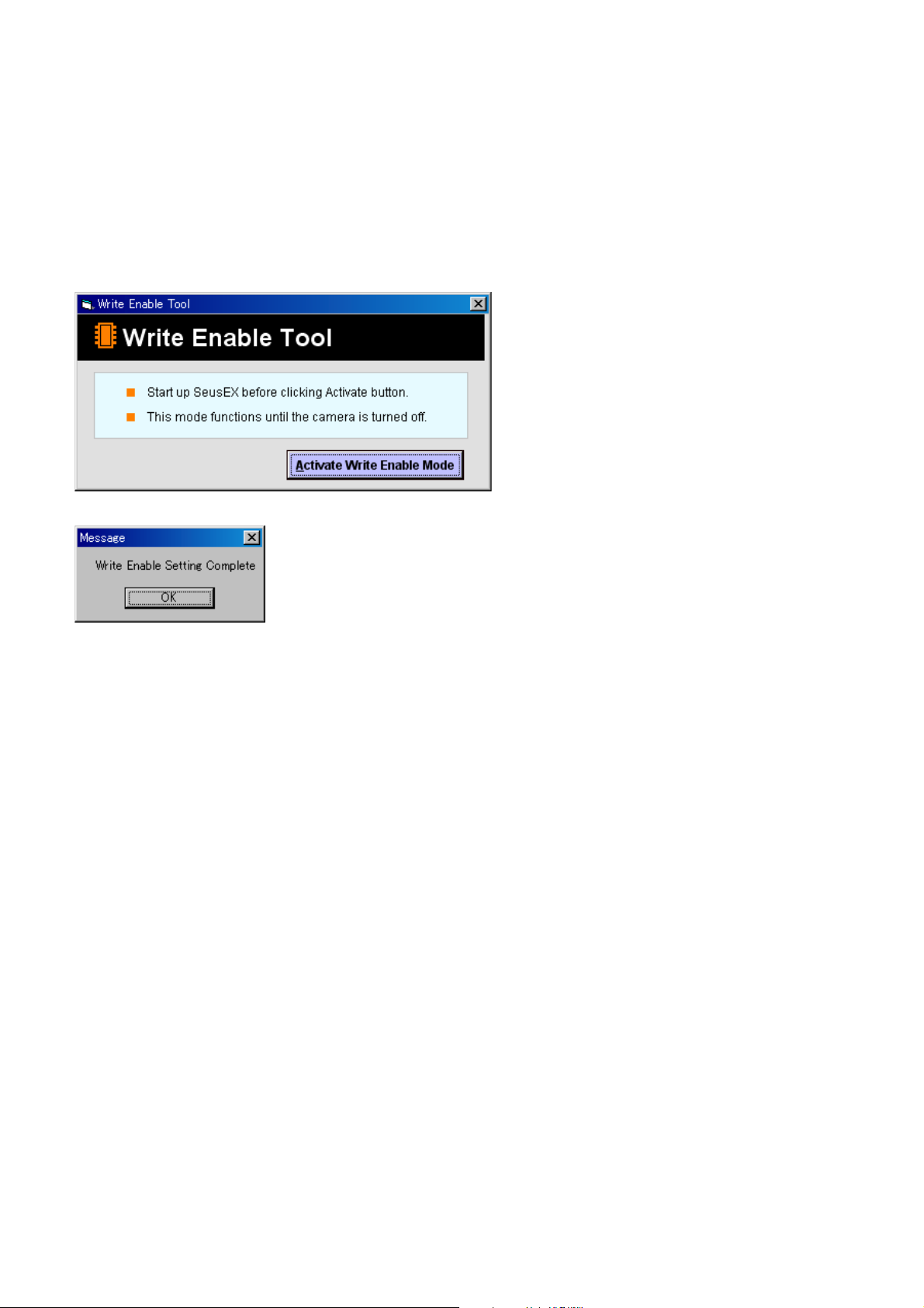
1-5. HOW TO WRITE DATA TO INTERNAL MEMORY
Usually, the camera has been set so as to disable the data writing from the PC to the internal memory of the camera.
This setting must be changed temporarily when the data is to be written to the internal memory such as a case after the board replacement.
To change the setting, use the write enable tool “WriteEnableTool.exe”.
Data writing method
1) Connect the PC to the camera (USB mode: Mass Storage), and switch the driver to the “Sony Seus USB Driver”.
2) Start the Write Enable Tool and the SeusEX.
3) Click the [Activate Write Enable Mode] button of the Write Enable Tool.
4) Upon completion of the setting change, the following message will be displayed.
5) Return the driver to the original one, and connect the PC to the camera (USB mode: Mass Storage).
6) Write the data read out into the PC to the internal memory of the camera.
7) Disconnect the PC from the camera, and turn off the camera.
Note: By turning off the camera, the write enable setting is reset.
DSC-W90_L2
1-4E
Page 8
NOTE FOR REPAIR
2. DISASSEMBLY
• Make sure that the flat cable and flexible board are not cracked of bent at the terminal.
Do not insert the cable insufficiently nor crookedly.
• When remove a connector, don’t pull at wire of connector. It is possible that a wire is snapped.
• When installing a connector, don’t press down at wire of connector.
It is possible that a wire is snapped.
• Do not apply excessive load to the gilded fle xible board.
Cut and remove the part of gilt
which comes off at the point.
(Be careful or some
pieces of gilt may be left inside)
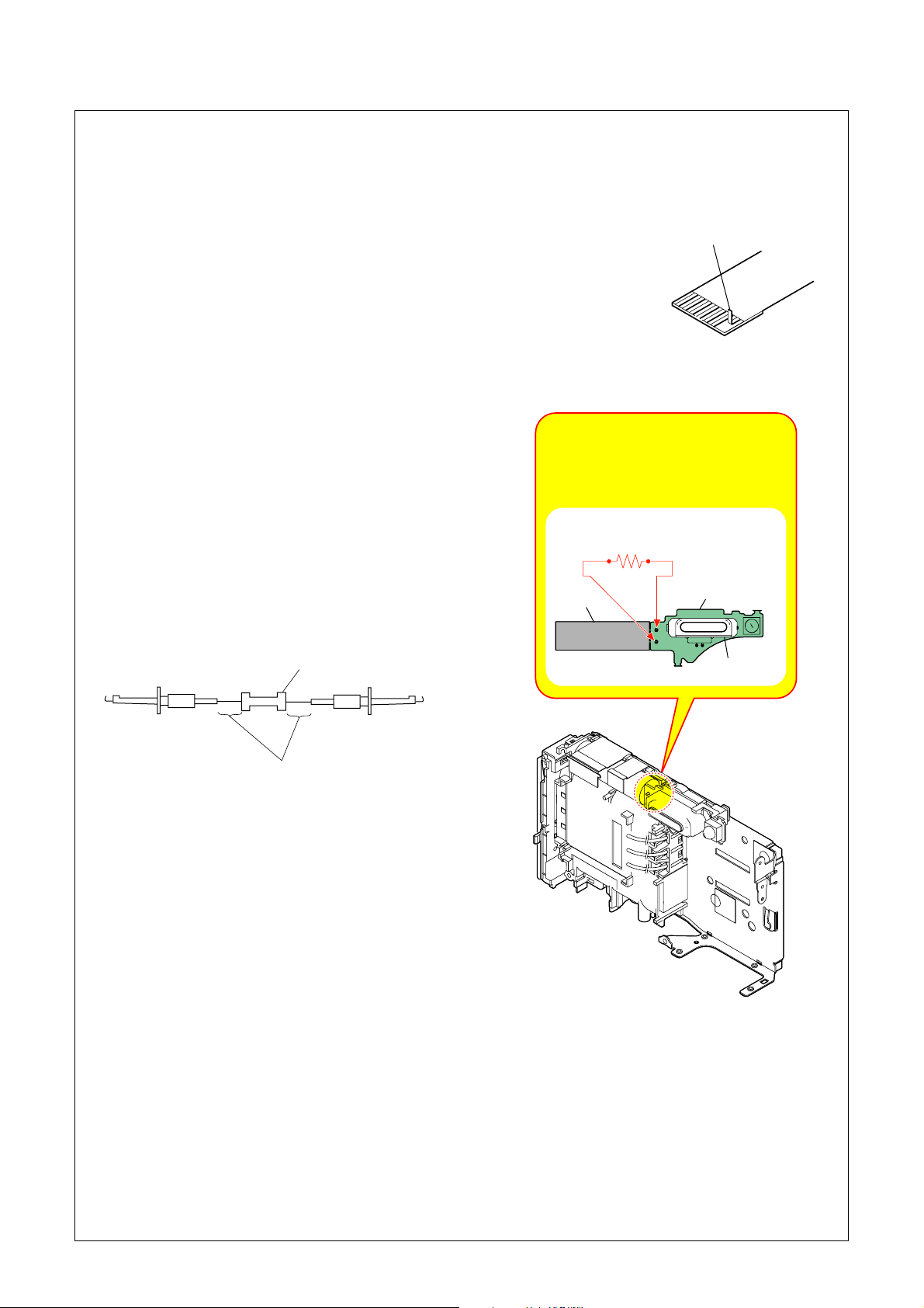
DISCHARGING OF THE ST-160 BOARD’S CHARGING CAPACITOR (C901)
The charging capacitor (C901) of the ST-160 board is charged
up to the maximum 300 V potential.
There is a danger of electric shock by this high voltage when the
capacitor is handled by hand. The electric shock is caused by
the charged voltage which is kept without discharging when the
main power of the unit is simply turned off. Therefore, the
remaining voltage must be discharged as described below.
Preparing the Short Jig
To preparing the short jig, a small clip is attached to each end of
a resistor of 1 kΩ /1 W (1-215-869-11).
Wrap insulating tape fully around the leads of the resistor to
prevent electrical shock.
Note: High-voltage cautions
Discharging the Capacitor
Short-circuit between the two points
with the short jig about 10 seconds.
R:1 kΩ/1 W
(Part code: 1-215-869-11)
C901
ST-160 Board
1 kΩ/1 W
Wrap insulating tape.
Flash Unit
DSC-W90_L2
2-1
Page 9
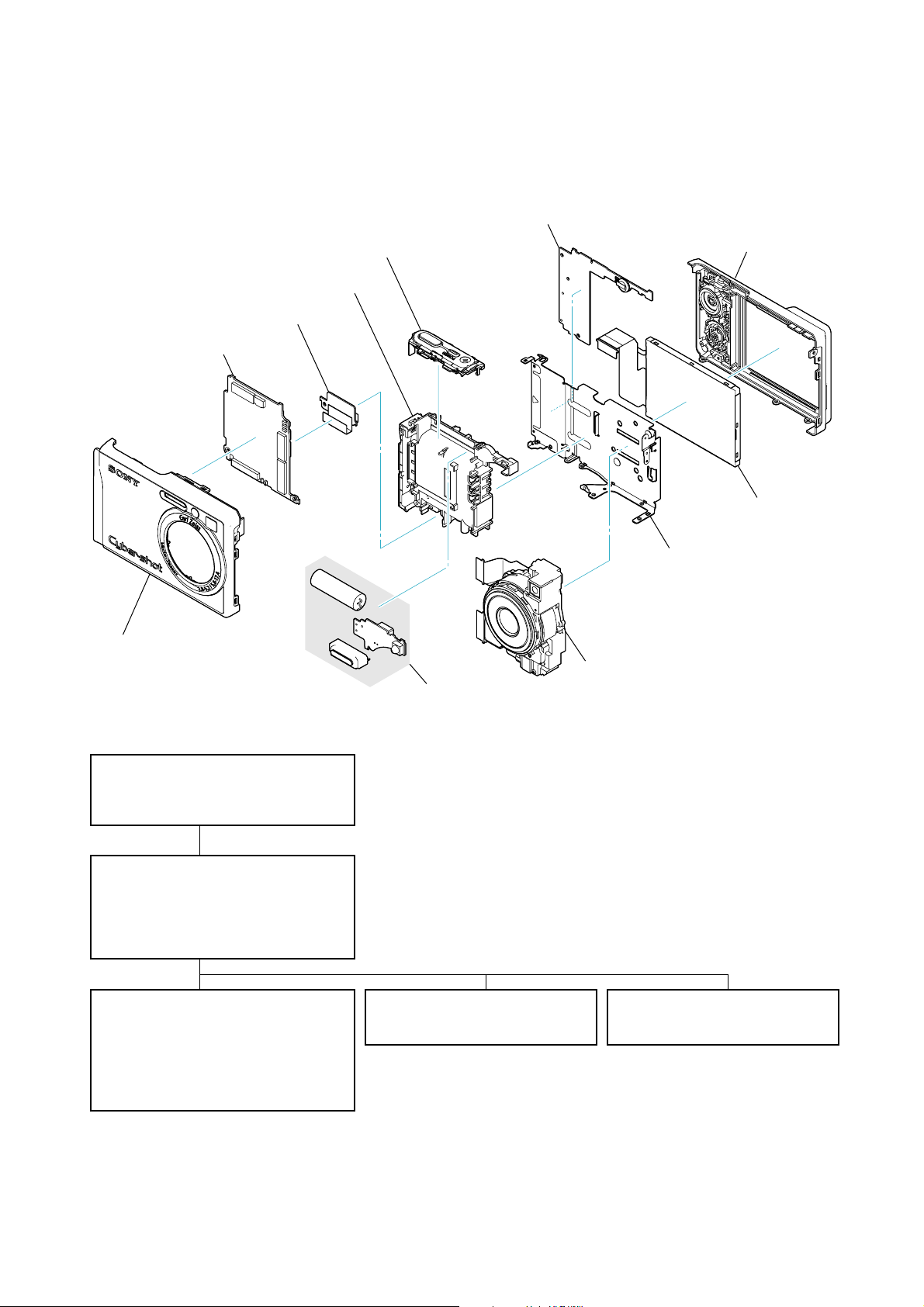
2-1. IDENTIFYING PARTS
Release Block
⋅ RL-071/078 Board
BT Holder
MC-176 Board
SY-169 Board
SW-494 Board
Cabinet (Rear)
LCD Module
Main Frame
Cabinet (Front)
- DISASSEMBLY FLOW -
2-2-1. CABINET SECTION
⋅ Cabinet (Front)
⋅ Cabinet (Rear)
2-2-2. MAIN BOARD SECTION
⋅ Lens Block
⋅ MC-176 Board
⋅ Release Block
⋅ SY-169 Board
2-2-3. LCD/BT HOLDER SECTION
⋅ BT Holder
⋅ Flash Unit
⋅ LCD Module
⋅ Main Frame
⋅ SW-494 Board
Flash Unit
⋅ ST-160 Board
2-3. EXCHANGE METHOD OF
BARRIER BLOCK
Lens Block
⋅ Barrier Block
⋅ Zoom Gear Block
2-4. EXCHANGE METHOD OF
ZOOM GEAR BLOCK
DSC-W90_L2
2-2
Page 10

EXPLODED VIEW
HELP
HELP
2-2. DISASSEMBLY
2-2-1. CABINET SECTION
Follow the disassembly in the numerical order given.
1 Cabinet (Front) (1-1 to 1-8)
2 Cabinet (Rear) (2-1 to 2-2)
Note:On installation of the cabinet (rear),
adjust the position of the mode dial
switch and the mode dial.
1-6 (#65)
1-7 (Open)
HARDWARE LIST
2-1 (#65)
HELP
1-5
(#65)
1-8
(Claw)
Main Board Section
(See Page 2-4)
1 Cabinet (Front)
1-4 (#65)
2 Cabinet
(Rear)
2-2 (#65)
1-1 (#65)
1-3
1-2 (Claw)
DSC-W90_L2
2-3
Page 11
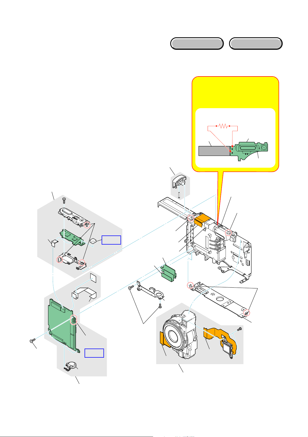
EXPLODED VIEW
2-2-2. MAIN BOARD SECTION
Follow the disassembly in the numerical order given.
1 Release Block (1-1 to 1-3)
2 Lens Block (2-1 to 2-5)
3 SY-169 Board (3-1 to 3-11)
HARDWARE LIST
Note: High-voltage cautions
Discharging the Capacitor
Short-circuit between the two points
with the short jig about 10 seconds.
R:1 kΩ/1 W
(Part code: 1-215-869-11)
1 Release Block
1-3
1-2
(Claw)
HELP
3-7 (Claw)
3-11
3-6
1-1
3-1
3-2
C901
ST-160 Board
Flash Unit
LCD/BT Holder
Section
(See Page 2-5)
2-3
(Release the claw
that is the fixation
of the flash unit
once)
3-5
(#3)
DSC-W90_L2
SY-169
3-3
3-4
(Solder)
HELP
3-10
3 SY-169 Board
3-8
(#5)
2-1
(Claw)
3-9
2-2
2-4
2-5
2 Lens Block
(See Page 2-6, 2-8)
2-4
Page 12
EXPLODED VIEW
2-2-3. LCD/BT HOLDER SECTION
Follow the disassembly in the numerical order given.
1 Flash Unit (1-1)
2 LCD Panel/SW-494 Board (2-1 to 2-4)
3 BT Holder (3-1 to 3-3)
HELP
2-1
(#5)
HARDWARE LIST
2 LCD Panel/
SW-494 Board
SW-494
2-4
(Claw)
1 Flash Unit
3-2
2-3
(Claw)
HELP
3-1 (#65)
2-2
(Claw)
HELP
3-3
1-1
(Claw)
3 BT Holder
DSC-W90_L2
2-5
Page 13
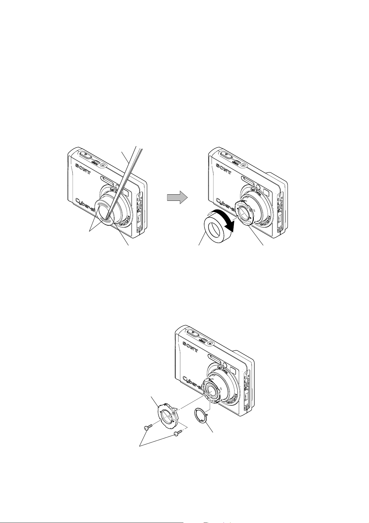
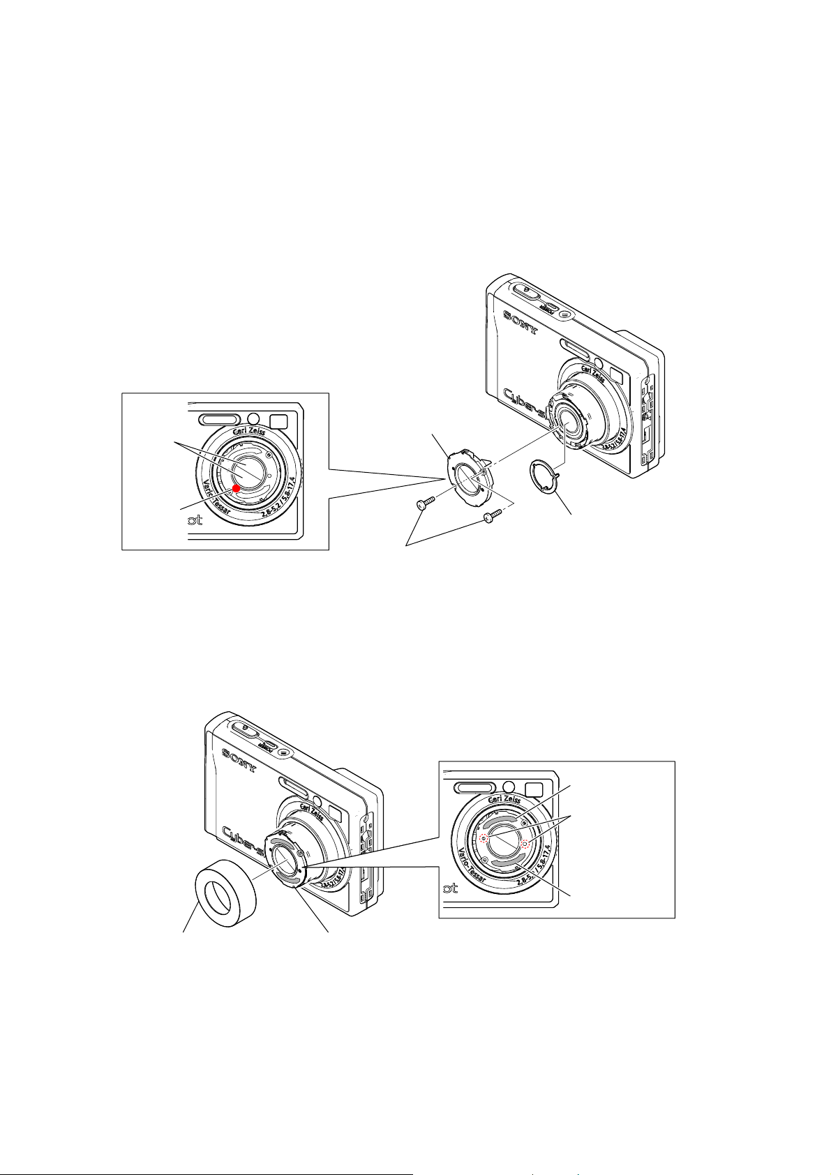
2-3. EXCHANGE METHOD OF BARRIER BLOCK
Note: Do not hold the part of spring.
2-3-1. HOW TO REMOVE THE ORNAMENTAL RING (A)
1 Turn on the power switch.
2 With the ornamental ring (A) extended, remove the battery forcibly.
3 Apply a solvent to the tweezers or a needle, and dissolve the adhesive on
the barrier tapes that secure the ornamental ring (A) to the barrier block.
4 Rotate the ornamental ring (A) clockwise to remove.
Tweezers
Barrier tape
3 Solvent
2-3-2. HOW TO REMOVE THE BARRIER BLOCK
1 Remove two screws.
2 Remove the barrier block and the inner ring.
2 Barrier block
4 Ornamental ring (A)
Barrier block
DSC-W90_L2
2 Inner ring
1 Two screws
2-6
Page 14
2-3-3. HOW TO INSTALL THE BARRIER BLOCK
1 Install the inner ring and the barrier block.
Note: When installing the barrier block, the CAV No. must be located in the lower left position.
2 Secure the barrier block with two screws.
*Tightening torque = 0.049 ± 0.01N • m (0.5 ± 0.1kgf • cm)
Note: Check that the barrier feather of the barrier block is not opened slightly or half-closed.
Barrier
1 Barrier block
feather
CAV No.
2 Two screws
2-3-4. HOW TO INSTALL THE ORNAMENTAL RING (A)
1 Affix two barrier tapes to the barrier block.
Note: The barrier tape must not cover the boss of the barrier block.
2 Install the ornamental ring (A).
1 Inner ring
1 Barrier tape
Boss
2 Ornamental ring (A)
Note: Turn on and off the power to check the opening and closing of the barrier block with the camera
in horizontal, up and down directions respectively.
Further, check the zoom motion.
Rotate the ornamental ring (A) lightly to check that it is not removed.
Barrier block
DSC-W90_L2
2-7
1 Barrier tape
Page 15

2-4. EXCHANGE METHOD OF ZOOM GEAR BLOCK
Note: Do not hold the part of terminal and the part of spring.
2-4-1. HOW TO REMOVE THE ZOOM GEAR BLOCK
• HOW TO REMOVE THE REAR ASSEMBLY
1 Remove the screw, and then the OVF.
OVF
Screw
2 Remove the shutter flexible board from the connector.
3 Remove the vibration-proof flexible board from the connector.
4 Peel the adhesive sheet that secures the vibration-proof flexible board.
*When peeling the adhesive sheet, turn it over from the opposite side of the hook.
Connector
2 Shutter flexible board
Connector
3 Vibration-proof flexible board
Vibration-proof flexible board
4 Adhesive
sheet
Hook
DSC-W90_L2
2-8
Page 16
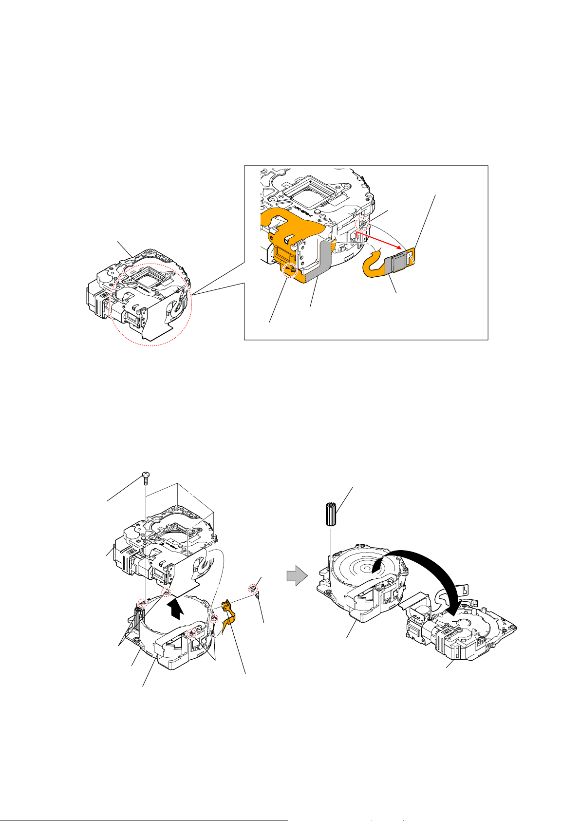
5 Peel the adhesive sheet (upper) that secures the main flexible board.
6 Disengage the main flexible board from the hook of the ring assembly, and then slide the main flexible board
to remove.
7 Peel the adhesive sheet (lower) that secures the main flexible board.
*The FOCUS motor must remain soldered.
6 Main flexible board
Hook
Ring assembly
5 Adhesive sheet (upper)
7 Adhesive sheet (lower)
Solder of FOCUS motor
8 Remove four screws that secure the rear assembly.
9 Remove the rear assembly, disengaging the bosses at four places.
*Take care not to get stuck with the vibration-proof flexible board.
q; Unhook the Z leaf spring to remove.
qa Remove the main flexible board from the ring assembly, and remove the rear assembly and the nuruto gear.
qa Nuruto gear
8 Five screws
Rear
assembly
Hook
9
q; Z leaf
Boss
Ring assembly
spring
Boss
Ring assembly
qa Rear assembly
qa Main flexible
Vibration-proof flexible board
board
DSC-W90_L2
2-9
Page 17

• HOW TO REMOVE THE ZOOM GEAR BLOCK
1 Unsolder the zoom motor.
2 Remove the FG leaf spring.
3 Remove the main flexible board from the zoom gear block.
4 Remove the zoom gear block.
Rear assembly
3 Main flexible board
4 Zoom gear block
3 Main flexible board
1 Solder
Hook
2 FG leaf spring
2-4-2. HOW TO INSTALL THE ZOOM GEAR BLOCK
• HOW TO INSTALL THE ZOOM GEAR BLOCK
1 Solder the main flexible board to the zoom gear block.
2 Install the main flexible board to the zoom gear block.
3 Attach the FG leaf spring.
Rear assembly
2 Main flexible board
Zoom gear block
DSC-W90_L2
1 Solder
2 Main flexible board
Hook
3 FG leaf spring
2-10
Page 18

4 Apply the lubricant (SRX-4339) to the nuruto gear, and insert it into the ring assembly.
* Rotate the gear in the ring assembly in the arrow direction until the end of the gear is not engaged
with a concave portion of the ring assembly (because a convex portion of the rear assembly enters
the convex portion).
Ring assembly
Gear
Convex portion
4 Nuruto gear
5 Install the zoom gear block on the rear assembly.
6 Engaging four bosses, install the rear assembly on the ring assembly.
*The vibration-proof flexible board must be engaged with the hook of the rear assembly.
7 Tighten four screws in the order of A to D.
*Tightening torque = 0.049 ± 0.01N • m (0.5 ± 0.1kgf • cm)
8 Check that the projection of the nuruto shaft that protrudes from the rear assembly is within the
specified value given below.
*Specified value: 0.005 – 0.395mm
Hook
Ring assembly
Boss
6 Vibration-proof
flexible board
DSC-W90_L2
Boss
Nuruto shaft
5 Zoom gear block
6 Rear assembly
Nuruto shaft
0.005 – 0.395mm
2-11
8
7 Four screws
B
C
D
A
Page 19

9 Secure and connect the main flexible board.
Ring assembly
Main flexible board
Hook
Main flexible board
Hook
Hook
Z leaf
spring
Adhesive sheet (upper)
Adhesive sheet (lower)
q; Secure and connect the vibration-proof flexible board and the shutter flexible board respectively.
Vibration-proof flexible board
Connector
Shutter flexible board
Connector
Bousin flexible board
Adhesive
sheet
Hook
DSC-W90_L2
2-12
Page 20

qa Install the OVF.
*When installing the OVF, fit a projection of OVF in the groove of the ring assembly.
OVF
Projection
Ring assembly
Groove
Screw
2-4-3. CHECK THE OPERATION
Confirm the operation after installing the lens block in the set.
1 Power ON/OFF
2 Expansion and contraction confirming of lens and opening and shutting confirmation of barrier.
Confirm there are neither dirt nor wounds in the surface of the ornamental ring (A) and lens
if there is no problem in operation.
Wipe off when dirty.
3 Confirm the operation with Wide/Tele.
Note: Do not be of caught etc.
Do not allophone.
DSC-W90_L2
2-13E
Page 21

HELP
Sheet attachment positions and procedures of processing the flexible boards/harnesses are shown.
Cabinet (front) assy
SY electrostatic sheet
RL-071/078
board
Harness (Red)
Light interception
sheet
Harness (Black)
Microphone
BT holder
Main frame
1mm
LC flexible sheet
DSC-W90_L2
HELP
Page 22

INSTALLATION METHOD OF BATTERY TERMINAL BOARD
1 Insert the battery terminal board into a slit in the BT holder to install.
*The battery terminal board is attached with the notch for installation.
BT holder
Battery terminal board
2 Fold the notch 3 or 4 times repeatedly to break.
Notch
Battery terminal
board
• HARNESS ARRANGEMENT
DSC-W90_L2
Notch
SY-169 board
Harness (Red)
Harness (White)
Harness (Black)
Notch
Battery terminal board
HELP
Page 23

3. BLOCK DIAGRAMS
Link
Link
OVERALL BLOCK DIAGRAM (1/2) POWER BLOCK DIAGRAM (1/2)
OVERALL BLOCK DIAGRAM (2/2)
POWER BLOCK DIAGRAM (2/2)
DSC-W90_L2
Page 24

3-1. OVERALL BLOCK DIAGRAM (1/2)
3. BLOCK DIAGRAMS
( ) : Number in parenthesis ( ) indicates the division number of schematic diagram where the component is located.
SHUTTER
MOTOR
M
LENS
ZOOM
FG
LENS BLOCK
ZOOM
MOTOR
FOCUS
MOTOR
M
FOCUS
RESET
SENSOR
ZOOM
RESET
SENSOR
OPTICAL IMAGE
STABILIZER
M
(METER)
YAW
MOTOR
PITCH
MOTOR
IRIS
IRIS
MOTOR
M
F_MOTOR_A, F_MOTOR_A(-),
F_MOTOR_B, F_MOTOR_B(-)
LENS TEMP
SENSOR
OIS TEMP
SENSOR
M
HALL
ELEMENT
M
HALL
ELEMENT
CD-694 FLEXIBLE BOARD
IC004
10
17 14
IC003
8.1M CCD
IMAGER
27 - 29
26 39
19 33
3 - 14
16, 15
31, 32
30 12
1 J4
24
ND(±) ND_±
Z_DC_MOTOR(±) ZOOM_A, ZOOM_A-
F_PI_SENS_OUT
XFC_RST_LED
Z_PI_SENS_OUT
XZM_FG_LED
LENS_ID
THERM
THERM
YAW±
YAW_HALL_BIAS±,
YAW_HALL_±
PITCH±
PITCH_HALL_BIAS±,
PITCH_HALL±
CN402
50, 49
38 - 3533 - 30
48 - 45
22
23
41
24, 28
26
44
40
4
15 - 1217 - 20
11 - 82, 3, 5, 6
BUFFER
B10, D10
G6, J8, J9, J7J3, J2, H2, J4
B1, D1
IC503
OPTICAL
IMAGE
STABILIZATION
DRIVE
(3/11)
SY-169 BOARD (1/2)
CN301
CCD_OUT
6
H1 - H3
35 - 37
LH
RG
V1, V2, V3A, V3B, V4,
V5A, V5B, V6 - V10
13 - 24
VST1, VST2
27, 26
VHLD1, VHLD2
11, 10
LV
SUB
29
SUB_CONT
31
FOCUS_A, A, B, B
J5
G5
C9
A7
A3
A5
A6
Q301
SWAOUT
CLK, DATA
D5, D6
SWBOUT
CA_FD
XDD_SYS_RST
A4, B4, B5
CLK_IC_503
XCS_IC_503
XIC_211_IC_503_RST
Q302
13
24, 25
10
D14
P7
P8
G4
C6
IC506
PITCH/YAW
SENSOR
AMP
(3/11)
L5, N4, N3, M2, L2, K4, K3
N5, P4, M4, N2, L3, L1, P5,
IC304
CCD SIGNAL
PROCESS,
P10, P9, P11
GENERATOR
F1, G2, E2, E1,
G1, D4, D3, F4,
J2, H4
H3, H1
LENS DRIVE
IRIS MOTOR
D2, B1
D6, E6, B7, C6
B4, B5
SHUTTER
F4, F3
21
1
K13
J13
TIMING
K14
(1/11)
E4, F3, D1, C2
D7 - D9
D10
IC401
D4
(2/11)
DRIVER
FOCUS
MOTOR
DRIVER
ZOOM
MOTOR
DRIVER
MOTOR
DRIVER
IC_211_0_SO, IC_211_0_SI, XIC_211_0_SCK
D3, F1
D5, A6, B6, C5
A2, C4, B2
G1, E4
SE501
YAW
SENSOR
SE502
PITCH
SENSOR
X201
36MHz
XCS_FE, XIC_211_3_SCK, IC_211_3_SO
FC_DIR_A, FC_DIR_B, FC_EN_A
ZM_DIR_A, ZM_EN_A, ZM_BRK_B
ZM_DC_FG_1A, ZM_DC_FG_1BZ_BOX2_PI_SENS_Col, Z_BOX1_PI_SENS_Col
XDD_SYS_RST
CA_AD00 - CA_AD13
CA_HD
CA_FD
GEN_TG_CLK
IC202
1
CLOCK
(9/11)
FC_SENS
LENS_ID
3
5
2
GENERATOR
XDD_SYS_RST
VSUB_CONT_PRE,
VSUB_CONT_POST
XLENS_DRIVER_PS
IRIS_M_IN, IRIS_M_BRK_2B
MSHUT_DIR, MSHUT_ENSHUTTER_±SHUTTER(±)
XFC_RST_LED
ZM_SENS_1ST
XZM_FG_LED
LENS_TEMP
TZ_HALL_TEMP
OVERALL (2/2)
(PAGE 3-2)
GEAR_ON
GEN_SYS_CLK
1
AF20, AE19, AF19, AE18
AC19, AC18, AE21, AF21, AE20,
AB21, AC21, AB20, AC20, AB19,
AE23
AF22
AF18
IC211
(1/2)
CPU
Y13
(4/11, 5/11)
Y12
V19, D19, C25
R7, AF25
H11
Y18, Y17
W18, AB26, W17
AB23, AA23, AC25
R8, AE25
Y10
M8
AD26
Y11, W11
L8
D9
AE3
AF3
W13
U8
H10
D17, B19, E17, A19,
U19
V8
AF8
AE8
T8
AB13
AF12
AC12
V7
A13 - A15,
E16, A18, D16, A17
B18, D18, B17
XIC_211_2_SCK
IC_211_AUOUT
VIDEO_AMP_ON
IC_211_CVOUT
VOUT_1
VOUT_2
XHD_EN
Y1, AA1 E18, B23
B13 - B15
LCD_CK, LCD_HD, LCD_VD
IC_211_2_SO, XIC_211_2_SCK
IC_211_2_SO,
XCS_AUDIO
IC_211_AUIN
Q242 - Q244
F3, E3
E4
E6
IC603
AUDIO AMP
E5
(7/11)
IC602
4
VIDEO AMP
(7/11)
Q241
BUFFER
USB_DP, USB_DM USB_DP, USB_DM
CLAMP
2
OVERALL (2/2)
(PAGE 3-2)
MSX_BS, MSX_D0 - MSX_D3, MSX_CLK
CN713
LCD_D0 - LCD_D7
XCS_ PANEL
XDD_SYS_RST
3 - 10
11 - 13
36
37
35, 3421, 22
D0 - D7
DCLK, HSYNC, VSYNC
SPENA
RESET Z
SPDA, SPCK
RL-071/078
BOARD (1/2)
CN101
(1/2)
17MIC_SIG
B6
A5, A2
CN707
(1/2)
1
MC-176 BOARD
(1/2)
CN710
AU_LINE_OUT A_OUT_L
D1
53
IC_211_YOUT HD Y3
IC_211_PROUT HD Pr16
(1/2)
24
V_LINE_OUT V_OUT
USB_VBUS USB_VBUS12
XMS_IN
26
28
17
15
19
CN704
6
2 - 5, 7, 8
CN101
(1/2)
5
10, 9
MEMORY
STICK
DUO
A : VIDEO SIGNAL
A : AUDIO SIGNAL
A : VIDEO/AUDIO SIGNAL
SP±
LCD901 (1/2)
LCD MODULE
2.5INCH
COLOR
LCD
MIC901
SP901
SPEAKER
16
20
HD Pb14IC_211_PBOUT
24
4
2
10, 12
6
CN102
(1/2)
MULTI
CONNECTOR
DSC-W90_L2
05
3-1
Page 25

3-2. OVERALL BLOCK DIAGRAM (2/2)
( ) : Number in parenthesis ( ) indicates the division number of schematic diagram where the component is located.
LCD901 (2/2)
LCD MODULE
BACKLIGHT
RL-071/078 BOARD (2/2)
S101
(SHUTTER)
S102
POWER
D101
(POWER)
SW-494 BOARD
S003
N
S001, S002,
S004 - S010
FUNCTION
KEY
S011
MODE
DIAL
D001
AE/AF LOCK/
SELF-TIMER
D002
FLASH CHARGING/
RECORD
BT001
LITHIUM
BATTERY
BL_H
BL_L BL_L
SY-169 BOARD (2/2)
CN101
(2/2)
8
XAE_LOCK_SW
7
XSHUTTER_SW
4
X_PWR_LED
CN001 CN708
XDIRECT_PB XDIRECT_PB8
KEY_AD1, 2 KEY_AD_1, 26, 7
MODE_DIAL1, 2 MODE_DIAL1, 212, 11
4 XAE_LOCK_LED XAE_LOCK_LED
5XSTRB_LED
1 VL_3V
9BL_L
12
8
7
3
4
5
9
8
4
CN707
(2/2)
7, 6
1, 2
XAE_LOCK_SW
XSHUT_SW
XPWR_ONXPWR_ON3
XPWR_LED
XSTRB_LED
VL_3V
2
OVERALL (1/2)
(PAGE 3-1)
Q006
BACKLIGHT
CONTROL
D101
XMS_IN
USB_VBUS
3
2
BL_EN2
XDIRECT_PB
IC102
BACK UP VCC
(8/11)
IC106
RESET
(8/11)
XPWR_ON
X101
32.768kHz
Q101
5
4
1
B8 H8
B7
J5
J4
IC101
FRONT
CONTROL
C6
(8/11)
D8
D7
A9
F9
B9
A1
B4
E2
D1, D2, E1
D102
XPWR_ON
UNREG
ST_UNREG
UNREG
CAM_12V
CAM_-7.5V
TI_5.0V
MAX_5.0V
D_3.0V
A_3.0V
DDR_1.8V
D_1.8V
D_1.2V
XPWR_OFF
XIC_211_RST_REQ
XDD_SYS_RST
XCS_FR
IC_211_0_SO,
IC_211_0_SI,
XIC_211_0_SCK
BL_H
IC001
DC/DC
CONVERTER
(10/11)
G8
W12
AB18
A23
H17, A24, G17
XACV_IN
K8
XACC_IN
G9
IC_211_1_UI, IC_211_1_UO
D26, G19
XCS_IC_201,
XIC_211_1_SCK,
IC_211_1_SO,
IC_211_1_SI
W20, H18, B24, G18
XDD_SYS_RST
Q004,
Q013
BATTERY
B1, B5, C5, D5
AUTHENTICATION
B2
IC201
(9/11)
XPOWER_ON
D002
D003
UART Rx, UART TX
E4
MC-176 BOARD
(2/2)
11 -13
8 - 10
6, 5
+
S
–
CN101
(2/2)
27
18 - 20
24
21 - 23
1
25, 26
TERMINAL
XPOWER_ON
ACV_UNREGACV_UNREG
CHARGE_VCHARGE_V
BT901
BATTERY
XACC_IN
UART Rx,
UART Tx
CN710
(2/2)
4
XACV_DET XACV_DET
XACC_IN
BATT_UNREG
BATT_SIG
7
30
7
19
26
23, 25
17, 21
15, 9
CN102
(2/2)
MULTI
CONNECTOR
FLASH
UNIT
ST-160 BOARD
XE_A(H)
TRIGGER
TRIG_GND
XE_K(L)
Q001
FLASH
DRIVE
+
C901
CHARGING
CAPACITOR
D001
T001
3 2
4
SELF-TIMER/
AF ILLUMINATOR
1
D002
ST_UNREG
15
1, 2
CONTROL,
CHARGE
CONTROL
7
IC001
FLASH
1
OVERALL (1/2)
XDD_SYS_RST
IC_211_0_SO, IC_211_0_SI, XIC_211_0_SCK
(PAGE 3-1)
XAE_LOCK_SW
XSHUT_SW
KEY_AD_1, 2
MODE_DIAL1, 2
XPWR_LED
XAE_LOCK_LED
XSTRB_LED
CN001
10
9
6
4
12
8
9
5
4
XAF_LED
STRB_CHG
XSTRB_FULL
STB_CHG_CNT
STRB_ON
CN701
12
8
9
5
AF LED
CONTROL
Q704
AFLED_CONT
D706
(MS ACCESS)
STRB_CHG
XSTRB_FULL
STB_CHG_CNT
STRB_ON14
N19
R19
AC8, AF6
AB7, AE6
Y9
W9
W8
G15
H8
V2
H9
H15
Y16
IC211
(2/2)
CPU
(4/11, 5/11)
DSC-W90_L2
05
3-2
Page 26

3-3. POWER BLOCK DIAGRAM (1/2)
( ) : Number in parenthesis ( ) indicates the division number of schematic diagram where the component is located.
CN102
MULTI
CONNECTOR
BT901
BATTERY
TERMINAL
+
S
–
ACV_UNREG
23, 25
XACV_DET
19
CHARGE_V
17, 21
XPOWER_ON
7
BATT_UNREG
BATT_SIG
A
POWER (2/2)
(PAGE 3-4)
B
POWER (2/2)
(PAGE 3-4)
C
POWER (2/2)
(PAGE 3-4)
D
POWER (2/2)
(PAGE 3-4)
SY-169 BOARD (1/2)MC-176 BOARD
CN101 CN710
18-20
24
21-23
27
XDD_SYS_RST
XIC_211_RST_REQ
XPWR_OFF
XPWR_ON
XDIRECT_PB
DDC2P9_EN
ACV_UNREG
11-138-10
XACV_DET
7
CHARGE_V BATT_UNREG
XPOWER_ON
4
XPWR_ON
D102
D003
AUTHENTICATION
TXRXE4
XRESET
B2
A9
CS
XSYS_RST
B4
A1
XRESET_REQ
B9
XPOWER_OFF
B8
XPOWER_ON0
XPOWER_ON2
B7
D002
IC201
BATTERY
(9/11)
P144_SOA0
P143_SIA0
P142_XSCKA0
P120_INTP0
IC106
RESET (8/11)
1 4
OUT Vdd
IC101
FRONT CONTROL
(8/11)
Q004, 013
IC_211_1_SI
D5
IC_211_1_SO
C5
XIC_211_1_SCK
B5
XCS_IC_201
B1
BATT_SENS
DDC2P9_AD
DDC1P8_AD
DDC1P2_EN D9
CAMDD_EN B2
DDC2P9_EN E9
BL_EN1 F8
BL_EN2 F9
DDC5PSW_EN F7
VSU_EN J8
DDC1P8_EN E8
DDCPV_EN C9
EVER_PSB J9
SW1P8_EN J1
LDO1P8_EN H2
DISW1P8_EN C2
DISW2P9_EN C1
XRSTX
DDC1P2_RESET
XACV_IN
D_3.0V
H8
H7
J7
D7
C8
F001
F002
E
POWER (2/2)
(PAGE 3-4)
D_3.0V
D_1.8V
BACK_UP_VCC
DDC1P2_EN
CAMDD_EN
DDC2P9_EN
BL_EN1
BL_EN2
DDC5PSW_EN
VSU_EN
DDC1P8_EN
DDCPV_EN
EVER_PSB
SW_1P8_EN
LDO_1P8_EN
DISW1P8_EN
DISW2P9_EN
1.2V_INT
L007
GD28
BATT45
PVSD13
PVBST29
PVLED35
LXSU47
PVAFE9
L002
IC001
DC/DC CONVERTER
(10/11)
LXSD
ONSD
LXBST
SWBST
ONBST
LXINV
PVINV
ONINV
LXLED
SWLED
FBLLED
ONLED
PVSU
ONSU
LXAFE
ONAFE
IC002
SW
9
VBAT
6
LBI
7
1
EN
PVM
LXM
ONM
SU
16
15
31
30
22
21
20
1
4
5
3
33
34
37
36
43
44
46
8
10
5V REG
(10/11)
VOUT
PS 8
Q706
B+ SWITCH
MS_PWR_ON
L009
DDC1P2_EN
L004
CAMDD_EN
L005
DDC2P9_EN
L003
BL_EN1
D011
VSU_EN
L006
DDC1P8_EN
2
EVER_PSB
D007
D010
D006
BL_EN2
DDC5PSW_EN
DDCPV_EN
SW_1P8_EN
LDO_1P8_EN
DISW1P8_EN
DISW2P9_EN
BACKLIGHT
CONTROL
B+ SWITCH
B+ SWITCH
IC003
Vin
B2
Q006
Q003
Q014
1.8V REG
Vcont
A2
(10/11)
Vout
D_3.0V
D_1.8V
Q007
1.8V/3.0V
(8/11)
VOUT
VRO
DISCHARGE
6VBAT3
8
Q010, 012
B+ SWITCH
B1
BACK_UP_VCC
BACK UP VCC
IC102
VCH
2
D101
7
VIN
XRESET
5
4
CS
POWER (2/2)
(PAGE 3-4)
EVER_3.0V
DETECTOR
1
Vout
F
IC007
VOLTAGE
(10/11)
Vsen
4
Vin
3
MS_VCC
ST_UNREG
CAM_-7.5V
L001
9
D_1.2V
CAM_12V
A_3.0V
D_3.0V
BL_H
BL_L
MAX_5.0V
TI_5.0V
D_1.8V
DDR_1.8V
VL_3V
CN704
MEMORY
STICK
DUO
G
POWER (2/2)
(PAGE 3-4)
DSC-W90_L2
05
3-3
Page 27

3-4. POWER BLOCK DIAGRAM (2/2)
SY-169 BOARD (2/2)
A_3.0V
D_1.8V
D_3.0V
MAX_5.0V
ST_UNREG
D_1.2V
CAM_12V
CAM_-7.5V
( ) : Number in parenthesis ( ) indicates the division number of schematic diagram where the component is located.
D_1.8V
D_3.0V
A
POWER (1/2)
(PAGE 3-3)
B2
IC501
2.8V REG
(3/11)
Vin
Vcont
A2
B1
Vout
B2 B1
XDD_SYS_RST
XIC_211_IC_503_RST
IC502
1.5V REG
(3/11)
Vin
Vout
XDD_SYS_RST
IC503
OPTICAL
IMAGE
STABILIZATION
DRIVE
(3/11)
RESET_NA7
XDLA6
IC506
PITCH/YAW
SENSOR AMP
(3/11)
SE502
PITCH
SENSOR
SE501
YAW
SENSOR
XDD_SYS_RST
BL_H
BL_L
POWER (1/2)
(PAGE 3-3)
LCD901
LCD MODULE
2.5INCH
COLOR
LCD
BACKLIGHT
D001
AE/AF LOCK/
SELF-TIMER
D002
FLASH CHARGING/
RECORD
FB702
L701
CN713
VDDD
VDD
PVDD
RESET Z
CN708
BL_H
BL_L
VL_3VVL_3V
D_3.0V
XDIRECT_PB
31
32
18
37
SW-494 BOARD
CN001
3
4
12
10
5
10
9
1
BT001
LITHIUM
BATTERY
3
8
S003
BL_H
BL_L
C
RL-071/078 BOARD
CN707
XPWR_ON
3
CN101
3
S102
POWER
G
POWER (1/2)
(PAGE 3-3)
A_3.0V
D_3.0V
BL_H
BL_L
MAX_5.0V
TI_5.0V
D_1.8V
DDR_1.8V
VL_3V
B
POWER (1/2)
(PAGE 3-3)
E
POWER (1/2)
(PAGE 3-3)
F
POWER (1/2)
(PAGE 3-3)
D_1.8V
D_3.0V
TI_5.0V
MAX_5.0V
A_3.0V
B2 B1Vin
IC601
2.8V REG
(7/11)
A_3.0V
D_3.0V
D_1.2V
DDR_1.8V
D_1.8V
XIC_211_RST_REQ
XPWR_OFF
XACV_IN
IC_211_1_SI
IC_211_1_SO
XIC_211_1_SCK
XCS_IC_201
MS_PWR_ON
Vout
R253
L241
FB281
FB282
FB283
GPE_09
H10
XRESET
AB18
W12
XRESET_REQ
GPE_00G8
GPE_05K8
SIO1_RXD
G18
SIO1_TXD
B24
SIO1_SCK
H18
GPS_04
W20
GPE_15
T7
IC211
CPU
(4/11)
(5/11)
(6/11)
AU_AVCC
TPU2_OUT
GPE_03 J8
G15
L211
R601
D601
R723
D_3.0V
D_1.8V
D_1.8V
D_3.0V
TI_5.0V
MAX_5.0V
A_3.0V
AFLED_CONT
CAM_3.5V
D
POWER (1/2)
(PAGE 3-3)
XZM_RST_LED
IC603
AUDIO AMP
(7/11)
IC602
VIDEO AMP
(7/11)
D706
(MS ACCESS)
IC202
CLOCK
GENERATOR
(9/11)
DDC2P9_EN
TI_5.0V
MAX_5.0V
TI_5.0V
D_3.0V
XDD_SYS_RST
D_3.0V
MAX_5.0V
A_3.0V
CAM_12V
CAM_-7.5V
3.5V REG
IC307
(1/11)
Vout B1
Vin
B2
Vcont
A2
2.3V REG
IC306
(1/11)
Vout
B2 B1Vin
Vout
6 4
Vin
IC308
2.8V REG
(1/11)
Q704
FB306
ST_UNREGST_UNREG
TI_5.0V
Q710
AF LED
DRIVE
AF LED
CONTROL
IC305
54
CAM_3.5V
Q305
2.8V/3.5V
DISCHARGE
13V REG
Vin
FB305
FB303
AF_5.0V
XAF_LED
(1/11)
Vout
FB302
TIMING GENERATOR
RESET
D10
D_3.0V
5
CN701 CN001
1, 2
3
11
12
IC304
CCD SIGNAL
PROCESS,
(1/11)
5
ST-160 BOARD
1, 2
3
11
AF ILLUMINATOR
12
B+ SWITCH
D101
(POWER)
D002
SELF-TIMER/
Q304
-7.5V
DISCHARGE
Q401
XZM_RST_LED
L303
L302
R402
R412
R411
R401
L001
IC001
FLASH CONTROL,
CHARGE CONTROL
CAM_12V
CAM_-7.5V
CN402
Z_PI_SENS_Vcc
Z_BOX1_PI_SENS_Vcc
Z_BOX2_PI_SENS_Vcc
F_PI_SENS_Vcc
IC401
LENS DRIVE
(2/11)
T001
D001
CD-694 FLEXIBLE
BOARD
CN301
1
9
42
27
25
21
FLASH
CCD IMAGER
BUFFER
LENS BLOCK
ZOOM
RESET
SENSOR
ZOOM
FG
FOCUS
RESET
SENSOR
UNIT
IC003
8.1M
IC004
05
DSC-W90_L2
3-4E
Page 28

4-1. FRAME SCHEMATIC DIAGRAM
4. PRINTED WIRING BOARDS AND SCHEMATIC DIAGRAMS
12
1
CN001
Note: CN001 is no mount.
(Direct solder)
SW-494
BOARD
BT001
LITHIUM BATTERY
MIC901
MICROPHONE
BLOCK
C901
CHARGING CAPACITOR
FLASH UNIT
1
ST-160 BOARD
11
CN001
122
FLEXIBLE FLAT CABLE
(FFC-093)
Note: CN701 is no mount.
(Direct solder)
2
12
CN701
1
11
(FFC-092)
FLEXIBLE FLAT CABLE
CN708
1
12
110
CN704
MEMORY STICK
CONNECTOR
RL-071/078 BOARD
LCD901
BACKLIGHT
LCD MODULE
2.5INCH
COLOR
LCD
BLK
RED
Note: CN101 is no mount.
CN101
18
(Direct solder)
LEVEL3
FLEXIBLE FLAT CABLE
(FFC-094)
RED
WHT
BLK
BT901
BATTERY
TERMINAL
39
1
39
38
11
LOCK
12
CN713
1
2
(Not supplied)
CN707
8
IC211
1
38
CN301
2
139
51
50
CN402
CD-694 FLEXIBLE BOARD
IC004
(Not supplied)
IC003
(Not supplied)
LENS BLOCK
DSC-W90_L2
LEVEL3
SY-169 BOARD
(SIDE A)
MC-176 BOARD (SIDE A)
26
2
25
CN102
1
27
28
MULTI CONNECTOR
4-1
130
CN710
BLK
RED
SP901
(FFC-095)
FLEXIBLE FLAT CABLE
130
CN101
Note: CN101 is no mount.
(Direct solder)
SPEAKER
MC-176 BOARD (SIDE B)
2
1
LEVEL3
SY-169 BOARD
(SIDE B)
FRAME
Page 29

Link
Link
4-2. SCHEMATIC DIAGRAMS
MC-176 BOARD (MULTI CONNECTOR)
SW-494 BOARD (CONTROL SWITCH)
COMMON NOTE FOR SCHEMATIC DIAGRAMS
ST-160 BOARD (FLASH DRIVE)
RL-071/078 BOARD
(CONTROL SWITCH, MIC)
DSC-W90_L2
Page 30

4-2. SCHEMATIC DIAGRAMS
4-2. SCHEMATIC DIAGRAMS
4-2. SCHEMATIC DIAGRAMS
THIS NOTE IS COMMON FOR SCHEMATIC DIAGRAMS
(In addition to this, the necessary note is printed in each block)
(For schematic diagrams)
• All capacitors are in µF unless otherwise noted. pF : µ
µF. 50 V or less are not indicated except f or electrolytics
and tantalums.
• Chip resistors are 1/10 W unless otherwise noted.
kΩ=1000 Ω, MΩ=1000 kΩ.
• Caution when replacing chip parts.
New parts must be attached after removal of chip.
Be careful not to heat the minus side of tantalum
capacitor, Because it is damaged by the heat.
• Some chip part will be indicated as follows.
Example C541 L452
22U 10UH
TA A 2520
Kinds of capacitor
External dimensions (mm)
Case size
• Constants of resistors, capacitors, ICs and etc with XX
indicate that they are not used.
In such cases, the unused circuits may be indicated.
•Parts with ★ differ according to the model/destination.
Refer to the mount table for each function.
• All variable and adjustable resistors have characteristic
curve B, unless otherwise noted.
• Signal name
XEDIT → EDIT PB/XREC → PB/REC
• 2: non flammable resistor
• 5: fusible resistor
• C : panel designation
• A : B+ Line
• B : B– Line
• J : IN/OUT direction of (+,–) B LINE.
• C : adjustment for repair.
• A : not use circuit
Precautions for Replacement of Imager
• If the imager has been replaced, carry out all the adjustments
for the camera section.
• As the imager may be damaged by static electricity from
its structure, handle it carefully like for the MOS IC.
In addition, ensure that the receiver is not covered with
dusts nor exposed to strong light.
1. Connection
Pattern box
Pattern box PTB-450
J-6082-200-A
or
Small pattern box
PTB-1450
J-6082-557-A
L = 24 cm (PTB-450)
L = 11 cm (PTB-1450)
Pattern box
Color bar chart
L
For PTB-450:
J-6020-250-A
For PTB-1450:
J-6082-559-A
Front of the lens
Camera
2. Adjust the distance so that the output waveform of
Fig. a and the Fig. b can be obtain.
H
Yellow
Cyan
White
Magenta
Green
AABBA=B
Fig. a (Video output terminal output waveform)
Fig.b (Picture on monitor TV)
Red
Blue
Electronic beam
scanning frame
CRT picture frame
DSC-W90_L2
When indicating parts by reference number, please
include the board name.
The components identified by mark 0 or dotted line with
mark 0 are critical for safety.
Replace only with part number specified.
Les composants identifiés par une marque 0 sont
critiques pour la sécurité.
Ne les remplacer que par une pièce portant le numéro
spécifie.
4-2
Page 31

Schematic diagrams of the CD-694 flexib le board and SY -169 board are not sho wn.
Pages from 4-3 to 4-14 are not shown.
DSC-W90_L2
Page 32

MC-176 BOARD
MULTI CONNECTOR
A
XX MARK:NO MOUNT
B
D
30
ACV_GND
ACV_GND
29
ACV_GND
UART TX
UART Rx
XACV_DET
REG_GND
HD Pr
REG_GND
HD Pb
REG_GND
USB_GND
USB_DP
USB_DM
USB_GND
A_GND
V_GND
HD Y
REG_GND
XACC_IN
28
27
26
25
24
23
22
21
20
19
18
17
16
15
14
13
12
11
10
9
8
7
6
5
4
3
2
1
CN101XX
USB_VBUS
USB_GND
USB_DP
USB_DM
USB_GND
AU_LINE_OUT
A_GND
V_OUT
V_GND
XPOWER_ON
CHARGE_V
CHARGE_V
CHARGE_V
ACV_UNREG
ACV_UNREG
ACV_UNREG
USB_VBUS
AU_LINE_OUT
V_LINE_OUT
Note: CN101 is not mounted. Flexible flat cable (FFC-095) is
soldered to this location instead.
This FFC-095 is not supplied, but this is included in
MC-176 complete board.
3421 8
5
6
7
Note:CN102 (multi connector) is not supplied,
but this is included in MC-176 complete board.
CN102
(MULTI CONNECTOR)
2
4
68
1012
14
16
1820
22
24
26
HD Pb
USB_VBUS
USB_GND
USB_DP
USB_DM
USB_GND
A_OUT_L
A_GND
V_OUT
V_GND
HD Y
XACC_IN
To AV/USB multi cable
ACV_GNDHD Pr
ACV_GND
ACV_GND
XPOWER_ON
UART Tx
UART Rx
CHARGE_V
XACV_DET
CHARGE_V
ACV_UNREG
ACV_UNREG
13
5
79
15
1719
21
23
25
A
B
CC
D
DSC-W90_L2
05
LND102
4-15
STATIC_GND
MC-176
Page 33

• Refer to page 4-2 for mark 0.
1 8
SW-494 BOARD
CONTROL SWITCH
A
XX MARK:NO MOUNT
Note: CN101 is not mounted. Flexible flat cable (FFC-092)
is soldered to this location instead.
CN001XX
1
VL_3V
D_3.0V
BL_L
BL_H
2
3
4
5
6
7
8
9
10
11
12
REG_GND
XAE_LOCK_LED
XSTRB_LED
B
LND001
LND004
KEY_AD1
KEY_AD2
XDIRECT_PB
MODE_DIAL2
MODE_DIAL1
STATIC_GND
STATIC_GND
XX
D003
BT001
(LITHIUM BATTERY)
SML-510MWT86S
5
4
XX
D005
3
2
1
D001
D002
SML-310YTT86
LND002
LND003
XX
D004
342
(AE/AF LOCK/SELF-TIMER)
(FLASH CHARGING/RECORD)
BL_L
BL_H
D001
D002
1
3
5
7
RB001
2200
5
6
7
A
RB003
2200
1
2
4
3
6
5
7
8
R001
2200
2
4
V
(SELF-TIMER)
2
4
1
3
1
3
S004
S005
S001
2
4
6
8
S002
B
(FLASH)
2
4
2
4
1
3
1
3
S006
S007
(DISP)
2
4
2
4
R005
2200
v
1
3
S008
b
(MACRO)
2
4
1
3
S010
z
(SET)
2
1
4
3
B
CC
1
1
3
S009
2
3
4
S011
AUTO
3
AUTO
4
HIGH SENS
5
SOFT SNAP
6
TWILIGHT PORTRAIT
7
TWILIGHT
8
LANDSCAPE
9
LANDSCAPE
10
BEACH
11
SNOW
12
MOVIE
13
PROGRAM AUTO
14
RB002
2200
1
2
4
R006
2200
R007
2200
3
6
5
7
8
Note: S011 (Mode dial) is not supplied,
but this is included in SW-494 complete board.
S003
W
(ZOOM)
T
MENU HOME
D
2
1
4
3
N
E
15
16
1
D
COM
2
COM
17
18
(MODE DIAL)
E
05
DSC-W90_L2
4-16
SW-494
Page 34

• Refer to page 4-2 for mark 0.
ST-160 BOARD
FLASH DRIVE
A
XX MARK:NO MOUNT
B
ST_UNREG
ST_UNREG
TI_5.0V
STRB_ON
STB_CHG_CNT
REG_GND
REG_GND
STRB_CHG
XSTRB_FULL
AF_5.0V
XAF_LED
CN00112P
NC
1
2
3
4
5
6
7
8
9
10
11
12
K1
K2
K3
CL-360S-TD4-X-TL
AF ILLUMINATOR
4
5
6
D002
SELF-TIMER/
3421 8
5
6
7
A
L001
2.2uH
2
1
1
SW
2
SW
3
VCC
4
F_ON
C001
22u
6.3V
C005
A3
3
A2
2
A1
1
XX
10V
220p
50V
C002
C007
D003
1u
R006
4700
RB520S-40TE61
T001
17
HGND
TPS65552RGTR
3
4
13
14
15
16
N.C
N.C
N.C
VBATT
PGND
IC001
PGND
XFULL
CHG
D001
MA2YF8000LS0
12
11
10
9
+
LND015
C901
315V 49uF
CHARGING
CAPACITOR
LND016
R005
LND019
XE_A(H)
C+
C-
XX
C006
10V
R004
1M
C004
0.047u
250V
R002
1M
5
6
7
8
CY25BAJ-8F-T23-G02
Q001
R003
100
1
2
3
4
LND017
TRIGGER
TRIG_GND
LND018
LND020
XE_K(L)
FLASH
UNIT
B
CC
XX
G_IGBT8N.C
I_PEAK
N.C
7
6
5
CL001
D
05
XE-L
XE-H
TRIGGERTRIGGER_GND
D
DSC-W90_L2
4-17
ST-160
Page 35

1
2
3
4
RL-071/078 BOARD
CONTROL SWITCH,MIC
A
XX MARK:NO MOUNT
B
XSHUTTER_SW
XAE_LOCK_SW
Note: CN101 is not mounted. Flexible
flat cable (FFC-094) is soldered
C
to this location instead.
MIC_SIG
MIC_GND
XPWR_ON
X_PWR_LED
D_3.0V
REG_GND
CN101XX
1
2
3
4
5
6
7
8
Note: In this set, either RL-071 or RL-078 board is used.
All mounted parts and schematic diagram are common
to both RL boards.
LND101
MIC_GND
MIC_SIG
LND102
2
1
4
3
S101
5
0.047u
2
3
C001
(SHUTTER)
6
4
1
(POWER)
D101
SML-412MWT86
S102
POWER
MIC901
MICROPHONE
BLOCK
C002
0.047u
A
B
C
LND103
LND104
D
05
STATIC_GND
STATIC_GND
D
DSC-W90_L2
4-18
RL-071/078
Page 36

Signal location of the SY-169 board is not shown.
Pages from 4-19 to 4-20 are not shown.
DSC-W90_L2
Page 37

Link
Link
4-4. PRINTED WIRING BOARDS
MC-176 BOARD
SW-494 BOARD
COMMON NOTE FOR PRINTED WIRING BOARDS
ST-160 BOARD
RL-071/078 BOARD
DSC-W90_L2
Page 38

4-4. PRINTED WIRING BOARDS
21321321
3
345
21
123
654
EB
C
3152
46
123
654
3152
46
123
54
43
12
312
45
534
12
14
23
4625
31
12
4
3
14
23
4-4. PRINTED WIRING BOARDS
4-4. PRINTED WIRING BOARDS
THIS NOTE IS COMMON FOR PRINTED WIRING BOARDS
• : Uses unleaded solder.
•
: Circuit board
: Flexible board
Pattern from the side which enables seeing.
: pattern of the rear side
(The other layers’ patterns are not indicated)
• Through hole is omitted.
• Circled numbers refer to waveforms.
• There are a few cases that the part printed on diagram
isn’t mounted in this model.
• C : panel designation
• Chip parts.
Transistor Diode
DSC-W90_L2
4-21
Page 39

Printed wiring boards of the CD-694 flexibile board and SY -169 board are not sho wn.
Pages from 4-22 to 4-24 are not shown.
DSC-W90_L2
Page 40

MC-176 (4 layers), SW-494 (2 layers)
CN001
BT001
LND001
112
–+
SW-494 BOARD (SIDE B)
1-871-501-
11
BT001
LITHIUM
BATTERY
Note: CN001 is not mounted. Flexible flat cable (FFC-092)
is soldered to this location instead.
05
12
: Uses unleaded solder.
MC-176 BOARD (SIDE A)
-
MC-176
>EP GW<
226
2728
05
CN102
(MULTI CONNECTOR)
Note: CN102 (multi connector) is not supplied,
but this is included in MC-176 complete board.
125
SW-494 BOARD (SIDE A)
AK
D001
D001
(AE/AF LOCK/SELF-TIMER)
D002
AK
(FLASH CHARGING/RECORD)
D002
A
1-871-499-
MC-176 BOARD (SIDE B)
CN101
11
LND102
05
1-871-499-
Note: CN101 is not mounted. Flexible flat cable (FFC-095) is
soldered to this location instead.
This FFC-095 is not supplied, but this is included in
MC-176 complete board.
W
42
130
(ZOOM)
13
S002
LND003
11
42
28
RB001
17
T
13
S005
Note: S011 (Mode dial) is not
supplied, but this is included
in SW-494 complete board.
LND002
N
42
S003
R007
13
14 13 2 12 11 10
45 6178
39
S011
1716
1815
S011
(MODE DIAL)
17
RB002
MENU
42
S007
13
R005
b
(MACRO)
42
S008
42
S009
13
HOME
05
28
28
RB003
17
13
z
13
5
4
D005
1
3
D003
AK
(SELF TIMER)
LND004
R006
v
(DISP)
S006
(SET)
42
S010
S001
42
V
42
B
(FLASH)
13
13
13
K
D004
1-871-501-
A
S004
R001
42
CAUTION
Danger of explosion if battery is incorrectly replaced.
Replace only with the same or equivalent type.
11 12
DSC-W90_L2
4-25
MC-176, SW-494
Page 41

ST-160 (4 layers), RL-071/078 (2 layers)
: Uses unleaded solder.
C901
CHARGING
CAPACITOR
ST-160 BOARD (SIDE A)
XE_K (L) XE_A (H)
C004
R004
LND016
1
D001
+
2
LND015
+
LND020
T001
05
LND018
D003
12
C002
1
1
C007
C005
2
2
43
12
C001
L001
ST-160 BOARD (SIDE B)
ST-160
R003
R002
05
5
4
Q001
8
1
FLASH UNIT
TRIG_GND TRIGGER
LND017
R006
CL001
CN001
14
IC001
17
516
813
11
11
12
12
12 9
C006
B
SELF-TIMER/
AF ILLUMINATOR
RL-071 BOARD (SIDE A)
LND103
65
2
C001
>EP GW<
R005
LND019
-
1-871-500-
05
11
1
(SHUTTER)
S101
S101
3
C002
4
RL-071 BOARD (SIDE B)
46
D002
13
1-871-500-
11
05
Note: In this set, either RL-071 or RL-078 board is used.
All mounted parts and schematic diagram are common to both RL boards.
>EP GW<
LND104
Note: CN101 is not mounted. Flexible flat cable (FFC-094)
is soldered to this location instead.
13
S102
POWER
-502-
1-871
S102
B
D101
KA
42
(POWER)
R
CN101
18
1-871-502-
MIC901
MICROPHONE
BLOCK
B
LND101 LND102
1-871-502-
RL-071
12
12
RL-078 BOARD (SIDE A)
LND103
1-874-109-
C001
05
(SHUTTER)
2
1
S101
65
3
S101
C002
4
RL-078 BOARD (SIDE B)
>EP GW<
LND104
05
A
-1091-874
13
S102
KA
42
(POWER)
S102
POWER
CN101
18
B
D101
RL-078
>EP GW<
R
B
RL-078
1-874-109-
MIC901
MICROPHONE
BLOCK
LND101LND102
1-874-109-
11
11
DSC-W90_L2
4-26E
Note: CN101 is not mounted. Flexible flat cable (FFC-094)
is soldered to this location instead.
ST-160, RL-071/078
Page 42

NOTE
NOTE
5. REPAIR PARTS LIST
NOTE: Characters A to Z of the electrical parts list indicate location of exploded views in which the desired part is shown.
Link
Link
CABINET SECTION
LENS SECTION
EXPLODED VIEWS
EXPLODED VIEWS
ABC
MAIN BOARD SECTION
D
LCD/BT HOLDER SECTION
Link
Link
MC-176 BOARD ST-160 BOARD SW-494 BOARD
RL-071/078 BOARD
ELECTRICAL PARTS LIST
ELECTRICAL PARTS LIST
BCC
B
ACCESSORIES
ACCESSORIES
DSC-W90_L2
Page 43

5. REPAIR PARTS LIST
5. REPAIR PARTS LIST
5. REPAIR PARTS LIST
NOTE:
• -XX, -X mean standardized parts, so they may have some differences from
the original one.
• Items marked “*” are not stocked since they are seldom required for routine
service. Some delay should be anticipated when ordering these items.
• The mechanical parts with no reference number in the exploded views are not
supplied.
• Due to standardization, replacements in the parts list may be different from
the parts specified in the diagrams or the components used on the set.
• CAPACITORS:
uF: µF
• COILS
uH: µH
• RESISTORS
All resistors are in ohms.
METAL: metal-film resistor
METAL OXIDE: Metal Oxide-film resistor
F: nonflammable
• SEMICONDUCTORS
In each case, u: µ, for example:
uA...: µA... , uP A... , µPA... ,
uPB... , µPB... , µPC... , µPC... ,
uPD..., µPD...
• Abbreviation
AR : Argentine model
AUS: Australian model
BR : Brazilian model
CH : Chinese model
CND : Canadian model
EE : East European model
HK : Hong Kong model
J: Japanese model
JE : Tourist model
KR : Korea model
NE : North European model
TW : Taiwan model
When indicating parts by reference number,
please include the board name.
The components identified by mark 0 or
dotted line with mark 0 are critical for safety.
Replace only with part number specified.
Les composants identifiés par une marque
0 sont critiques pour la sécurité.
Ne les remplacer que par une pièce portant
le numéro spécifié.
• Color Indication of Appearance Parts
Example:
(SILVER) : Cabinet’s Color
(Silver) : Parts Color
DSC-W90_L2
5-1
Page 44

5. REPAIR PARTS LIST
DISASSEMBLY
5. REPAIR PARTS LIST
5-1. EXPLODED VIEWS
5-1-1. CABINET SECTION
#65
2
HARDWARE LIST
4
#65
7
5
6
#65
5
#65
1
#65
#65
Lens/Main Board Section
(See Page 5-3)
3
Ref. No. Part No. Description Ref. No. Part No. Description
1 X-2177-048-1 CABINET (FRONT) ASSY (SILVER)
1 X-2177-049-1 CABINET (FRONT) ASSY (BLACK)
* 2 3-197-910-01 SHEET, SY ELECTROSTATIC
3 3-099-623-01 CABINET, SIDE
4 X-2177-059-1 CABINET (REAR) ASSY (SILVER)
DSC-W90_L2
4 X-2177-060-1 CABINET (REAR) ASSY (BLACK)
5 3-099-626-01 SHEET, LCD WINDOW ADHESIVE
6 3-099-624-01 WINDOW, LCD
7 3-099-625-01 PLATE, MODE
#65 2-635-591-01 SCREW (M1.4), NEW TRUSTAR P2 (Silver)
5-2
Page 45

5-1-2. MAIN BOARD SECTION
DISASSEMBLY
ns: not supplied
#65
5. REPAIR PARTS LIST
5. REPAIR PARTS LIST
60
HARDWARE LIST
59
52
#3
57
51
54
ns
(FFC-093)
ns
SY-169
SP901
55
58
ns
56
MIC901
53
(Note 1)
#5
#5
64
Lens Section
(See Page 5-5)
63
61
62
LCD/BT Holder Section
(See Page 5-4)
65
66
#30
68
(including IC003 (CCD imager) and
CD-694 flexible complete board) (Note 2)
Note 1: In this set, either RL-071 or RL-078 board is used.
Ref. No. Part No. Description Ref. No. Part No. Description
51 A-1253-157-A SY-169 BOARD, COMPLETE (SERVICE)
52 3-099-637-01 LABEL, FUSE
* 53 3-099-634-01 SHEET, ST INSULATING
* 54 3-099-636-01 SHEET, RL INSULATING
55 3-099-620-01 RETAINER, RELEASE
56 A-1246-054-A RL-071 BOARD, COMPLETE (Note 1)
56 A-1271-235-A RL-078 BOARD, COMPLETE (Note 1)
57 1-833-618-11 CABLE, FLEXIBLE FLAT (FFC-094)
58 X-2177-054-1 RELEASE ASSY
59 3-099-621-01 CABINET, UPPER
60 3-099-622-01 SHAFT, STRAP
61 A-1246-051-A MC-176 BOARD, COMPLETE
* 62 3-099-639-01 SHEET, MC RADIATION
* 63 3-099-629-01 RETAINER, MULTI
DSC-W90_L2
All mounted parts and schematic diagram are common to both RL boards.
Note 2: Be sure to read “Precuations for Replacement of
Imager” of level 3 on page 4-2.
* 64 3-099-635-01 SHEET, MC INSULATING
65 3-099-632-01 CABINET BOTTOM (SILVER)
65 3-099-632-11 CABINET BOTTOM (BLACK)
66 3-113-705-01 SHEET (PLUS), CD RADIATION
68 A-1253-767-A CCD BLOCK ASSY (including IC003 (CCD
IMAGER) and CD-694 flexible complete board)
(Note 2)
MIC901 1-542-721-11 MICROPHONE BLOCK
SP901 1-826-614-21 LOUD SPEAKER (1.0CM)
#3 2-660-401-01 SCREW (M1.7), NEW TRU-STAR, P2 (Red)
#5 3-080-204-01 SCREW, TAPPING, P2 (Black)
#30 3-086-156-11 SCREW B1.2 (White)
#65 2-635-591-01 SCREW (M1.4), NEW TRUSTAR P2 (Silver)
5-3
Page 46

5-1-3. LCD/BT HOLDER SECTION
DISASSEMBLY
5. REPAIR PARTS LIST
5. REPAIR PARTS LIST
HARDWARE LIST
ns: not supplied
105
104
106
#65
103
#5
110
107
111
ns
108
109
BT001
!
: BT001 (BATTERY, LITHIUM
SECONDARY)
Board on the mount position.
(See page 4-25)
LCD901
C901
ns
112
102
101
• Refer to page 5-1 for mark 0.
Ref. No. Part No. Description Ref. No. Part No. Description
101 A-1246-052-A ST-160 BOARD, COMPLETE
0 102 1-480-014-11 FLASH UNIT
* 103 3-113-323-01 LABEL, MS CAUTION
104 3-099-631-01 SCREW, TRIPOD
105 3-099-627-01 FRAME, MAIN
106 3-099-633-01 SHEET, LC FLEXIBLE
* 107 3-100-059-01 SHEET, LC FLEXIBLE ADHESIVE
* 108 3-197-557-01 SHEET, LIGHT INTERCEPTION
109 A-1246-053-A SW-494 BOARD, COMPLETE
* 110 3-100-060-01 SHEET, SW
BT901
(Note)
113
111 1-833-616-11 CABLE, FLEXIBLE FLAT (FFC-092)
* 112 3-198-159-01 SHEET, BT TERMINAL
113 X-2177-056-1 HOLDER ASSY, BT
0 BT001 1-756-710-11 LITHIUM RECHARGEABLE BATTERY
BT901 A-1257-452-A TERMINAL, SERVICE (BT) (Note)
0* C901 1-114-309-11 ELECT 49uF 315V
LCD901 1-802-379-11 LCD MODULE (LQ025A3DD01)
#5 3-080-204-01 SCREW, TAPPING, P2 (Black)
#65 2-635-591-01 SCREW (M1.4), NEW TRUSTAR P2 (Silver)
Note: Ref e r to HELP “Installation method of battery termi-
nal board” when changing the service terminal (BT).
Danger of explosion if battery is incorrectly replaced.
Replace only with the same or equivalent type.
CAUTION
DSC-W90_L2
5-4
Page 47

5-1-4. LENS SECTION
ns: not supplied
5. REPAIR PARTS LIST
5. REPAIR PARTS LIST
151
155
(Note 2)
ns
ns
HARDWARE LIST
#30
#30
154
(Note 1)
ns
153
152
(Note 1)
Note 1: Be sure to read “Exchange method of barrier b lock”
(Note 1)
#30
on page 2-6.
M901 (Note 2)
157
(Note 2)
ns
156
(Note 2)
Note 2: Be sure to read “Exchange method of zoom gear
block” on page 2-8.
Ref. No. Part No. Description Ref. No. Part No. Description
151 A-1231-924-A LSV-1160A (SERVICE)
152 2-689-851-01 RING (A), ORNAMENTAL (Note 1)
153 2-691-890-01 TAPE, BARRIER (Note 1)
154 A-1205-001-A BARRIER BLOCK ASSY (Note 1)
155 2-689-849-01 SPRING, Z LEAF (Note 2)
156 2-689-850-01 SPRING, FG LEAF (Note 2)
157 2-689-871-01 GEAR, NARUTO (Note 2)
M901 1-479-864-11 GEAR BLOCK, ZOOM (1160) (Note 2)
#30 3-086-156-11 SCREW B1.2 (White)
DSC-W90_L2
5-5
Page 48

Electrical parts list of the CD-694 flexible
board is not shown.
Page 5-6 is not shown.
DSC-W90_L2
Page 49

MC-176 RL-071 RL-078 ST-160 SW-494
5-2. ELECTRICAL PARTS LIST
Ref. No. Part No. Description Ref. No. Part No. Description
A-1246-051-A MC-176 BOARD, COMPLETE
***********************
(Flexible flat cable (FFC-095) and CN102 are not supplied,
but they are included in MC-176 complete board.)
(Not supplied) CABLE, FLEXIBLE FLAT (FFC-095)
< CONNECTOR >
CN102 (Not supplied) CONNECTOR, MULTIPLE (SOCKET)
(MULTI CONNECTOR)
A-1246-054-A RL-071 BOARD, COMPLETE
A-1271-235-A RL-078 BOARD, COMPLETE
**********************
Note: In this set, either RL-071 or RL-078 board is used.
All mounted parts and schematic diagram are common to both RL boards.
IC001 6-707-555-01 IC TPS65552RGTR
* L001 1-400-820-11 INDUCTOR 2.2uH
0*Q001 6-551-452-01 TRANSISTOR CY25BAJ-8F-T23-G02
R002 1-218-989-11 RES-CHIP 1M 5% 1/16W
R003 1-218-941-11 RES-CHIP 100 5% 1/16W
0 R004 1-216-121-11 RES-CHIP 1M 5% 1/10W
R006 1-218-961-11 RES-CHIP 4.7K 5% 1/16W
< IC >
< COIL >
< TRANSISTOR >
< RESISTOR >
< TRANSFORMER >
1-833-618-11 CABLE, FLEXIBLE FLAT (FFC-094)
< CAPACITOR >
C001 1-119-923-11 CERAMIC CHIP 0.047uH 10% 10V
C002 1-119-923-11 CERAMIC CHIP 0.047uH 10% 10V
< DIODE >
D101 6-501-030-01 DIODE SML-412MWT86 (POWER)
< MICROPHONE >
MIC901 1-542-721-11 MICROPHONE BLOCK
< SWITCH >
* S101 1-786-912-21 TACTILE SWITCH (SHUTTER)
S102 1-786-885-42 SWITCH, TACTILE (POWER)
A-1246-052-A ST-160 BOARD, COMPLETE
**********************
0 1-480-014-11 FLASH UNIT
< CAPACITOR >
C001 1-100-611-91 CERAMIC CHIP 22uF 20% 6.3V
C002 1-112-717-91 CERAMIC CHIP 1uF 10% 6.3V
0 C004 1-100-758-11 CERAMIC CHIP 0.047uF 10% 250V
C007 1-164-933-11 CERAMIC CHIP 220PF 10% 50V
0*C901 1-114-309-11 ELECT 49uF 315V
< CONNECTOR >
CN001 1-779-330-51 FFC/CONNECTOR, FPC (LIF (NON-ZIF)) 12P
< DIODE >
0*D001 6-501-433-01 DIODE MA2YF8000LS0
* D002 6-501-861-01 DIODE CL-360S-TD4-X-TL
(SELF-TIMER/AF ILLUMINATOR)
D003 6-500-619-01 DIODE RB520S-40TE61
0 T001 1-445-108-21 TRANSFORMER, D.C-D.C CONVERTER
A-1246-053-A SW-494 BOARD, COMPLETE
**********************
(S011 (mode dial) is not supplied, but this is included
in SW-494 complete board.)
1-833-616-11 CABLE, FLEXIBLE FLAT (FFC-092)
* 3-100-060-01 SHEET, SW
< LITHIUM BATTERY >
0 BT001 1-756-710-11 LITHIUM RECHARGEABLE BATTERY
< DIODE >
D001 8-719-075-29 DIODE SML-510MWT86S
(AE/AF LOCK/SELF-TIMER)
D002 8-719-077-34 DIODE SML-310YTT86
(FLASH CHARGING/RECORD)
< RESISTOR >
R001 1-218-957-11 RES-CHIP 2.2K 5% 1/16W
R005 1-218-957-11 RES-CHIP 2.2K 5% 1/16W
R006 1-218-957-11 RES-CHIP 2.2K 5% 1/16W
R007 1-218-957-11 RES-CHIP 2.2K 5% 1/16W
< COMPOSITION CIRCUIT BLOCK >
RB001 1-234-376-11 RES, NETWORK 2.2K (1005X4)
RB002 1-234-376-11 RES, NETWORK 2.2K (1005X4)
RB003 1-234-376-11 RES, NETWORK 2.2K (1005X4)
< SWITCH >
S001 1-786-885-42 SWITCH, TACTILE (V (SELF-TIMER))
S002 1-786-885-42 SWITCH, TACTILE (W (ZOOM))
S003 1-786-885-42 SWITCH, TACTILE (N)
S004 1-786-885-42 SWITCH, TACTILE (B (FLASH))
S005 1-786-885-42 SWITCH, TACTILE (T (ZOOM))
S006 1-786-885-42 SWITCH, TACTILE (v (DISP))
S007 1-786-885-42 SWITCH, TACTILE (MENU)
S008 1-786-885-42 SWITCH, TACTILE (b (MACRO))
• Refer to page 5-1 for mark 0.
DSC-W90_L2
Danger of explosion if battery is incorrectly replaced.
CAUTION
Replace only with the same or equivalent type.
5-7
Page 50

Ref. No. Part No. Description Ref. No. Part No. Description
S009 1-786-885-42 SWITCH, TACTILE (HOME)
S010 1-786-885-42 SWITCH, TACTILE (z (SET))
S011 (Not supplied) ROTARY SWITCH (MODE DIAL)
Electrical parts list of the SY-169 board is
not shown.
Pages 5-9 to 5-13 are not shown.
SW-494
DSC-W90_L2
5-8
Page 51

Checking supplied accessories.
Note 1: This item is supplied with the unit as an accessory , but
is not prepared as a service part.
Battery Charger
BC-CSGB
0 1-479-791-22 (US, CND)
USB, A/V Cable for
Multi-use T erminal
1-829-866-41
Battery Charger
BC-CSGB
0 1-479-791-32
(EXCEPT US, CND,
E: Latin America, BR)
BC-CSGC
0 1-480-175-31
(E: Latin America)
Power Cord
0 1-555-074-91 (AUS)
0 1-782-476-71 (CH)
0 1-823-947-71 (KR)
0 1-827-269-31 (UK, HK)
0 1-827-826-41 (AEP, E)
0 1-832-106-31 (AR)
Other accessories
3-095-004-11 MANUAL, INSTRUCTION (ENGLISH) (EXCEPT US, BR)
3-095-004-21 MANUAL, INSTRUCTION (FRENCH, ITALIAN) (CND, AEP)
3-095-004-31 MANUAL, INSTRUCTION (SPANISH, PORTUGUESE)
(AEP, E, AR)
3-095-004-41 MANUAL, INSTRUCTION (GERMAN, DUTCH) (AEP)
3-095-004-51 MANUAL, INSTRUCTION
(TRADITIONAL CHINESE, SIMPLIFIED CHINESE)
(E, HK, CH)
3-095-004-61 MANUAL, INSTRUCTION (RUSSIAN) (AEP)
3-095-004-71 MANUAL, INSTRUCTION (ARABIC, PERSIAN) (E)
3-095-004-81 MANUAL, INSTRUCTION (KOREAN) (KR)
3-095-004-91 MANUAL, INSTRUCTION (POLISH, CZECH) (AEP)
3-095-005-11 MANUAL, INSTRUCTION (HUNGARIAN, SLOVAK) (AEP)
3-095-005-21 MANUAL, INSTRUCTION (SWEDISH, FINNISH) (AEP)
3-095-005-31 MANUAL, INSTRUCTION (NORWEGIAN, DANISH) (AEP)
3-095-005-41 MANUAL, INSTRUCTION (THAI, MALAY) (E)
3-095-005-51 MANUAL, INSTRUCTION (TURKISH, GREEK) (AEP)
3-095-005-61 MANUAL, INSTRUCTION (ENGLISH, SPANISH) (US)
3-094-994-01 HANDBOOK (PDF) (JAPANESE) (Note 2)
3-094-994-11 HANDBOOK (PDF) (ENGLISH) (Note 2)
3-094-994-21 HANDBOOK (PDF) (FRENCH) (Note 2)
3-094-994-31 HANDBOOK (PDF) (ITALIAN) (Note 2)
3-094-994-41 HANDBOOK (PDF) (SPANISH) (Note 2)
3-094-994-51 HANDBOOK (PDF) (PORTUGUESE) (Note 2)
3-094-994-61 HANDBOOK (PDF) (GERMAN) (Note 2)
3-094-994-71 HANDBOOK (PDF) (DUTCH) (Note 2)
3-094-994-81 HANDBOOK (PDF) (TRADITIONAL CHINESE) (Note 2)
3-094-994-91 HANDBOOK (PDF) (SIMPLIFIED CHINESE) (Note 2)
Rechargeable Battery Pack
NP-BG1
(Note 1)
Wrist Strap
2-050-981-01
Conversion (2P) Adaptor
0 1-569-008-12 (E: NTSC)
Battery Case
(Note 1)
CD-ROM
(Cyber-shot Application Software/
“Cyber-shot Handbook”/
“Cyber-shot Step-up Guide”)
3-094-911-01 (EXCEPT US)
3-196-435-01 (US)
3-094-995-11 HANDBOOK (PDF) (RUSSIAN) (Note 2)
3-094-995-21 HANDBOOK (PDF) (ARABIC) (Note 2)
3-094-995-31 HANDBOOK (PDF) (PERSIAN) (Note 2)
3-094-995-41 HANDBOOK (PDF) (KOREAN) (Note 2)
3-094-995-51 HANDBOOK (PDF) (POLISH) (Note 2)
3-094-995-61 HANDBOOK (PDF) (CZECH) (Note 2)
3-094-995-71 HANDBOOK (PDF) (HUNGARIAN) (Note 2)
3-094-995-81 HANDBOOK (PDF) (SLOVAK) (Note 2)
3-094-995-91 HANDBOOK (PDF) (SWEDISH) (Note 2)
3-094-996-11 HANDBOOK (PDF) (FINNISH) (Note 2)
3-094-996-21 HANDBOOK (PDF) (NORWEGIAN) (Note 2)
3-094-996-31 HANDBOOK (PDF) (DANISH) (Note 2)
3-094-996-41 HANDBOOK (PDF) (THAI) (Note 2)
3-094-996-51 HANDBOOK (PDF) (MALAY) (Note 2)
3-094-996-61 HANDBOOK (PDF) (TURKISH) (Note 2)
3-094-996-71 HANDBOOK (PDF) (GREEK) (Note 2)
Note 2: Handbooks (PDF) of each language are included in
CD-ROM (Cyber-shot Application Software).
• Refer to the page 5-1 for mark 0.
DSC-W90_L2
5-14E
Page 52

HARDWARE LIST (1/4)
#1: M1.7 X 2.5
(Black)
2-635-562-11
2.5
#5: M1.7 X 3.5 (Tapping)
(Black)
3-080-204-01
3.5
#9: M1.7 X 5.0 (Tapping)
(Silver)
3-078-890-21
1.7
1.7
#2: M1.7 X 4.0
(Black)
2-635-562-31
#6: M1.4 X 1.7
(Silver)
2-598-474-01
#10:M1.7 X 4.0
(Silver)
2-599-475-31
4.0
1.7
1.4
1.7
#3: M1.7 X 2.5
(Red)
2-660-401-01
2.5
#7: M1.7 X 1.6
(Black)
7-627-552-18
1.6
#11:M1.7 X 4.0 (Tapping)
(Silver)
3-078-890-11
1.7
1.7
#4: M1.4 X 2.5 (Tapping)
(Dark Silver)
3-348-998-81
1.4
2.5
#8: M1.7 X 3.5 (Tapping)
(Silver)
3-078-890-01
1.7
3.5
#12:M1.7 X 5.0 (Tapping)
(Black)
3-080-204-21
5.0
#13:M1.7 X 2.5 (Tapping)
(Silver)
3-085-397-01
2.5
#17:M1.7 X 1.5
(Silver)
2-586-389-01
1.7 2.2
1.5
3.5
1.7
1.7
#14:M1.7 X 2.5
(Silver)
2-599-475-11
#18:M1.4 X 2.5
(Silver)
2-635-591-21
4.0
2.5
2.5
1.7
1.4
1.7
4.0
#15:M1.4 X 1.5
(Silver)
3-062-214-01
1.5
#19:M1.2 X 4.0 (Tapping)
(Red)
3-086-156-21
4.0
1.4
1.7
1.2
1.7
5.0
#16:M1.4 X 2.5
(Silver)
2-586-337-01
1.4
2.5
#20:M1.4 X 3.0
(Silver)
2-635-591-31
1.4
3.0
Page 53

HARDWARE LIST (2/4)
#21:M1.4 X 3.0
(Black)
2-662-396-21
#25:M1.7 X 3.0
(Black)
2-635-562-21
#29:M1.4 X 2.5
(Black)
2-662-396-01
3.0
3.0
1.4
1.7
#22:M1.7 X 5.0 (Tapping)
(Silver)
3-083-261-01
5.0
#26:M1.4 X 2.0
(Silver)
2-635-591-11
2.0
#30:M1.2 X 4.0 (Tapping)
(White)
3-086-156-11
1.7
1.4
#23:M1.7 X 4.0 (Tapping)
(Black)
3-080-204-11
4.0
#27:M1.4 X 2.0
(Black)
2-662-396-11
2.0
#31:M3.0 X 4.0
(Silver)
2-102-434-01
1.7
1.4
#24:B1.7 X 5.5 (Tapping)
(Black)
4-679-805-11
1.7
5.5
#28:M1.4 X 4.0 (Tapping)
(Dark Silver)
3-348-998-61
1.4
4.0
#32:M2.0 X 4.5 (Tapping)
(Silver)
2-102-498-01
2.5
#33:M3.0 X 6.0
(Silver)
3-077-331-21
6.0
#37:M2.0 X 6.0 (Tapping)
(Black)
3-080-206-31
6.0
3.0
1.4
2.0
3.5
#34:M3.0 X 8.0
(Black)
3-077-331-41
8.0
#38:M3.0 X 20.0 (Tapping)
(Silver)
7-685-651-79
20.0
3.0
1.2
3.0
4.0
#35:M4.0 X 6.0 (Tapping)
(Silver)
3-975-291-02
6.0
#39:M2.6 X 5.0 (Tapping)
(Black)
7-685-791-09
5.0
4.0
2.6
3.0
2.0
4.5
#36:M3.0 X 6.0
(Silver)
4-886-821-11
3.0
6.0
#40:M2.0 X 4.0 (Tapping)
(Silver)
7-685-851-04
2.0
4.0
Page 54

HARDWARE LIST (3/4)
#41:M3.0 X 8.0 (Tapping)
(Silver)
3-065-748-01
8.0
#45:M1.4 X 2.5
(Silver)
2-587-151-01
2.5
#49:M2.0 X 4.0
(Black)
2-630-005-31
3.0
1.4
#42:M2.0 X 4.0 (Tapping)
(Silver)
7-628-253-00
4.0
#46:M1.7 X 3.0
(Red)
2-660-401-11
3.0
#50:M2.0 X 3.0
(Red)
2-891-494-11
1.7
2.0
#43:M1.7 X 4.0
(Red)
2-660-401-31
4.0
#47:M1.4 X 3.0 (Tapping)
(Silver)
2-665-774-01
3.0
#51:M2.0 X 2.5
(Silver)
3-073-686-01
1.7
1.4
#44:M1.7 X 3.0 (Tapping)
(Silver)
3-078-890-61
1.7
3.0
#48:M1.7 X 2.5
(Silver)
3-973-497-91
1.7
2.5
#52:M2.0 X 4.0 (Tapping)
(Black)
3-080-206-11
4.0
#53:M2.0 X 5.0 (Tapping)
(Black)
3-080-206-21
5.0
#57:M1.7 X 4.0
(Black)
7-627-852-18
4.0
2.0
1.7
2.0
3.0
#54:M1.75 X 6.0 (Tapping)
(Black)
3-318-203-11
6.0
#58:M2.0 X 6.0 (Tapping)
(Silver)
3-719-408-11
6.0
2.0
1.75
2.0
2.5
#55:M2.0 X 4.0
(Silver)
2-655-582-11
4.0
#59:M2.0 X 5.0 (Tapping)
(Silver)
3-080-205-21
5.0
2.0
2.0
2.0
2.0
4.0
#56:M2.0 X 3.5
(Silver)
3-067-187-11
2.0
3.5
#60:M2.6 X 5.0
(Black)
3-061-062-11
2.6
5.0
Page 55

HARDWARE LIST (4/4)
#61:M3.0 X 10.0
(Black)
7-682-549-09
#65:M1.4 X 3.5
(Silver)
2-635-591-01
#69:M1.7 X 3.0
(Silver)
2-599-475-21
10.0
3.5
3.0
1.4
#62:M2.0 X 3.0
(Silver)
3-080-202-21
#66:M1.4 X 1.4
(Silver)
2-635-591-41
#70:M1.7 X 5.0
(Silver)
2-599-475-41
3.0
1.4
1.4
2.0
#63:M5.0 X 12.5
(Black)
3-060-811-21
#67:M1.4 X 2.0
(Silver)
3-389-523-16
#71:M1.4 X 2.0
(Red)
3-208-537-01
2.0
12.5
5.0
1.4
#64:M1.7 X 5.0 (Tapping)
(Silver)
2-666-551-21
1.7
5.0
#68:M1.7 X 4.0
(Silver)
2-655-581-01
1.7
4.0
3.0
1.7
5.0
1.7
1.4
2.0
Page 56

[Description of main button functions on toolbar of the Adobe Acrobat Reader Ver5.0 (for Windows)]
Toolbar
Printing a text
1. Click the Print button .
2. Specify a printer, print range, number of copies, and other options, and then click [OK].
Application of printing:
To set a range to be printed within a page, select the g raphic
selection tool
be printed, and then click the Print button.
and drag on the page to enclose a range to
Finding a text
1. Click the Find button .
2. Enter a character string to be found into a text box, and click
the [Find]. (Specify the find options as necessary)
Application to the Service Manual:
To execute “find” from current page toward the pre vious pages,
select the check box “Find Backward” and then click the
“Find”.
3. Open the find dialog box again, and click the [Find Again] and
you can find the matched character strings displayed next.
(Character strings entered previously are displayed as they are
in the text box.)
Reversing the screens displayed once
•To reverse the previous screens (operation) one by one, click
.
the
•To advance the reversed screens (operation) one by one, click
.
the
Application to the Service Manual:
This function allows you to go and back between circuit diagram and printed circuit board diagram, and accordingly it
will be convenient for the voltage check.
Moving with link
1. Select either palm tool , zoom tool , text selection tool
, or graphic selection tool .
2. Place the pointer in the position in a text where the link exists
(such as a button on cover and the table of contents page, or
blue characters on the removal flowchart page or drawing
page), and the pointer will change to the forefinger form .
3. Then, click the link. (You will go to the link destination.)
Moving with bookmark:
Click an item (text) on the bookmark pallet, and you can move
to the link destination. Also, clicking can display the
hidden items.
(To go back to original state, click )
Application to the Service Manual:
The parts on the drawing pages (block diagrams, circuit diagrams, printed circuit boards) and parts list pages in a text
can be found using this find function. For example, find a
Ref. No. of IC on the block diagram, and click the [Find Again]
continuously, so that you can move to the Ref. No. of IC on
the circuit diagram or printed circuit board diagram successively.
Note: The find function may not be applied to the Service
Manual depending on the date of issue.
Switching a page
•To move to the first page, click the .
•To move to the last page, click the
•To move to the previous page, click the
•To move to the next page, click the
.
.
.
Zooming or rotating the screen display
“Zoom in/out”
• Click the triangle button in the zoom control box to select the
display magnification. Or, you may click
ing in or out.
“Rotate”
• Click rotate tool , and the page then rotates 90 degrees each.
or for zoom-
Application to the Service Manual:
The printed circuit board diagram you see now can be changed
to the same direction as the set.
Page 57

Reverse
985219231.pdf
Revision History
Ver.
1.0
Date
2007.02
History
Official Release
Contents
—
S.M. Rev.
issued
—
DSC-W90_L2
 Loading...