

Page 1
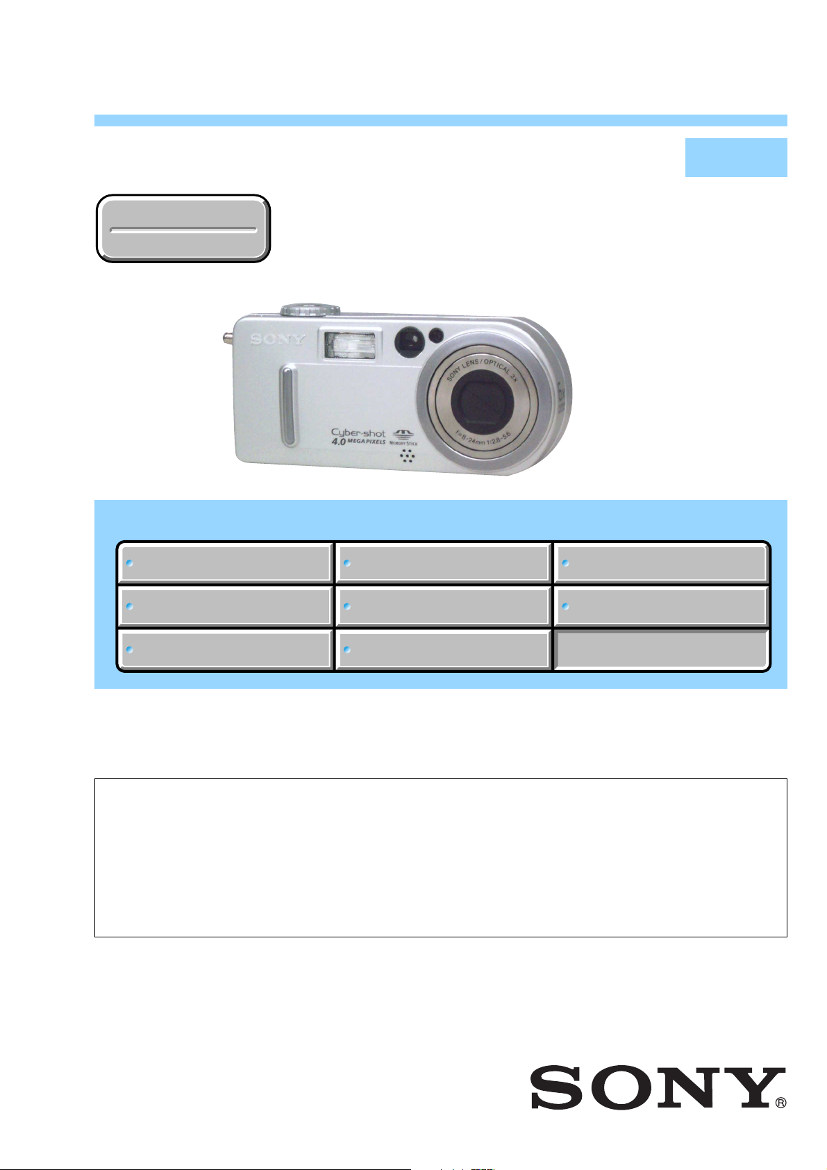
DSC-P7
SERVICE MANUAL
Ver 1.1 2002. 10
Revision History
Revision History
Link
Link
SPECIFICATIONS
SPECIFICATIONS
BLOCK DIAGRAMS
BLOCK DIAGRAMS
LEVEL 2
US Model
Canadian Model
AEP Model
UK Model
E Model
Hong Kong Model
Australian Model
Chinese Model
Korea Model
Tourist Model
Japanese Model
PRINTED WIRING BOARDS
PRINTED WIRING BOARDS
SERVICE NOTE
SERVICE NOTE
DISASSEMBLY
DISASSEMBLY
• For ADJUSTMENTS (SECTION 6), refer to SERVICE MANUAL, ADJ (992997651.pdf).
• For INSTRUCTION MANUAL, refer to SERVICE MANUAL, LEVEL 1 (992997641.pdf).
• This service manual contains information for Japanese model as well.
• Note in Lens Frame Installation
On the JK-226, JK-227 and SY-77 boards
This service manual procides the information that is premised
the circuit board replacement service and not intended repair
inside the JK-226, JK-227 and SY-77 boards.
Therefore, schematic diagram, printed wiring board and
electrical parts list of the JK-226, JK-227 and SY-77 boards are
not shown.
The following pages are not shown.
FRAME SCHEMATIC DIAGRAMS
FRAME SCHEMATIC DIAGRAMS
SCHEMATIC DIAGRAMS
SCHEMATIC DIAGRAMS
JK-226, JK-227 boards
Schematic diagram ......................... Pages 4-33 to 4-34
Printed wiring board ........................ Pages 4-49 to 4-50
Electrical parts list ........................... Pages 5-6
SY-77 board
Schematic diagram ......................... Pages 4-9 to 4-28
Printed wiring board ........................ Pages 4-43 to 4-46
Electrical parts list ........................... Pages 5-9 to 5-13
The above-described information is shown in service
manual Level 3.
REPAIR PARTS LIST
REPAIR PARTS LIST
DIGITAL STILL CAMERA
Page 2

DSC-P7
COVER
COVER
SPECIFICATIONS
System
Image device
Total pixels number of camera
Lens 3 × zoom lens
8.93 mm (1/1.8 type) color
CCD
Primary col or filter
Approx. 3 340 000 pixels
17
/
−
32
15
/16 inches)
−
16
4 19/32 inches))
24.0 mm (5/
f=8
−
(35 mm camera conversion: 39 to
117mm (1
5.6
F2.8
−
Camera
Effective pixels number of camera
Exposure control
White balance
File format Still images: DCF conformity
Recording media
Flash Recommended distance
Approx. 3 210 000 pixels
Automatic,
Scene selection (three modes)
Automatic, D a ylight, Cloudy,
Fluorescent, Incandescent
(Exif Ver. 2.2, JPEG conformity
GIF at Clip Mot ion)
DPOF correspondence
Movies: MPEG1 conformity
(Monaural)
Audio with s till image: MPEG1
conformity (Monaural)
“Memory Stick”
0.5 to 3.8 m (1.6 to 12.5 ft) (W)
0.6 to 2.4 m (2 to 7.9 ft) (T)
(when ISO sensitivity is set to Auto)
Output connectors
A/V OUT (MONO) jack
USB jack mini-B
Minijack
Video: 1 Vp-p, 75
sync negative
Audio: 327 mV (at a 47 k
Output impedance 2.2 k
Ω
, unbalanced,
Ω
load)
Ω
LCD screen
LCD panel used
Total number of dots
3.8 cm (1.5 type) TFT drive
123 200 (560×220) dots
Power, general
Used battery pack
Power requirement s
Power consumption (when shooting)
Operating temperature range
Storage te mperature range
Dimensions 114 × 51.5 × 35.8 mm
Mass 206 g (7 oz) (NP-FC10 battery pack,
Microphone Electret condenser microphone
Speaker Dynamic speaker
NP-FC10
3.6 V
1.9W
+
40°C (32° to +104°F)
0° to
20° to +60°C (−4° to +140°F)
−
1
/2 × 2 × 1 3/8 i nches)
(4
(W/H/D, protruding portions not
included)
“Memory Stick” and wrist strap
included)
AC-LS1A AC power adaptor
Power requireme nts
Rated output voltage
Operating temperature rang e
Storage temperature range
Dimensions 105 × 36 × 56 mm (4
Mass Approx. 180 g (6 oz)
AC 100 – 240 V, 50/60 Hz
DC 4.2 V, 1.5 A
+
40°C (32° to +104°F)
0° to
−
20° to +60°C (−4° to +140°F)
1
/4 inches) (W/H/D, protruding
2
parts not included)
(adaptor only)
1
/4 × 1 7/16 ×
NP-FC10 battery pack
Used battery Lithium ion battery
Maximum voltage
Nominal v olt age
Capacity 2.4 Wh (675 mAh)
DC 4.2 V
DC 3.6 V
Accessories
• A/V connecting cable (1)
• NP-FC10 battery pack (1)
• AC-LS1A AC power adaptor (1)
• Power cord (mains lead) (1)
• USB cable (1)
• Wrist strap (1)
• “Memor y Stick” (16MB) (1)
• CD-ROM (USB driver: SPVD-008) (1)
• Operating Instructions (1)
Design and specifications are subject to change
without notice.
— 2 —
Page 3

DSC-P7
SAFETY-RELATED COMPONENT WARNING!!
COMPONENTS IDENTIFIED BY MARK 0 OR DOTTED LINE WITH
MARK 0 ON THE SCHEMATIC DIAGRAMS AND IN THE PARTS
LIST ARE CRITICAL TO SAFE OPERATION. REPLACE THESE
COMPONENTS WITH SONY PARTS WHOSE PART NUMBERS
APPEAR AS SHOWN IN THIS MANUAL OR IN SUPPLEMENTS
PUBLISHED BY SONY .
SAFETY CHECK-OUT
After correcting the original service problem, perform the following
safety checks before releasing the set to the customer.
1. Check the area of your repair for unsoldered or poorly-soldered
connections. Check the entire board surface for solder splashes
and bridges.
2. Check the interboard wiring to ensure that no wires are
"pinched" or contact high-wattage resistors.
3. Look for unauthorized replacement parts, particularly
transistors, that were installed during a previous repair. Point
them out to the customer and recommend their replacement.
4. Look for parts which, through functioning, show obvious signs
of deterioration. Point them out to the customer and
recommend their replacement.
5. Check the B+ voltage to see it is at the values specified.
6. Flexible Circuit Board Repairing
• Keep the temperature of the soldering iron around 270˚C
during repairing.
• Do not touch the soldering iron on the same conductor of the
circuit board (within 3 times).
• Be careful not to apply force on the conductor when soldering
or unsoldering.
ATTENTION AU COMPOSANT AYANT RAPPORT
À LA SÉCURITÉ!
LES COMPOSANTS IDENTIFÉS P AR UNE MARQUE 0 SUR LES
DIAGRAMMES SCHÉMA TIQUES ET LA LISTE DES PIÈCES SONT
CRITIQUES POUR LA SÉCURITÉ DE FONCTIONNEMENT. NE
REMPLACER CES COMPOSANTS QUE PAR DES PIÈSES SONY
DONT LES NUMÉROS SONT DONNÉS DANS CE MANUEL OU
DANS LES SUPPÉMENTS PUBLIÉS PAR SONY.
Unleaded solder
Boards requiring use of unleaded solder are printed with the leadfree mark (LF) indicating the solder contains no lead.
(Caution: Some printed circuit boards may not come printed with
the lead free mark due to their particular size.)
: LEAD FREE MARK
Unleaded solder has the following characteristics.
• Unleaded solder melts at a temperature about 40°C higher than
ordinary solder.
Ordinary soldering irons can be used but the iron tip has to be
applied to the solder joint for a slightly longer time.
Soldering irons using a temperature regulator should be set to
about 350°C.
Caution: The printed pattern (copper foil) may peel away if the
heated tip is applied for too long, so be careful!
• Strong viscosity
Unleaded solder is more viscous (sticky, less prone to flow) than
ordinary solder so use caution not to let solder bridges occur such
as on IC pins, etc.
• Usable with ordinary solder
It is best to use only unleaded solder but unleaded solder may
also be added to ordinary solder.
— 3 —
Page 4

DSC-P7
TABLE OF CONTENTS
Section Title Page Section Title Page
1. SERVICE NOTE ························································1-1
Self-diagnosis Display····················································· 1-3
2. DISASSEMBLY
2-1. BT Lid ·············································································2-2
2-2. Cabinet (Front) Assembly ···············································2-2
2-3. Cabinet (Rear) Assembly················································· 2-3
2-4. LCD Module····································································2-3
2-5. Cabinet (Bottom) Assembly ············································2-4
2-6. Lens Block Assembly······················································2-4
2-7. Control Switch block·······················································2-5
2-8. SY-77 Board ···································································· 2-6
2-9. Memory Stick Connector ················································2-6
2-10. ST-70 Board····································································· 2-7
2-11. SW-368 Board ·································································2-7
2-12. JK-227 Board ··································································2-8
2-13. Circuit Boards Location ·················································· 2-9
3. BLOCK DIAGRAMS
3-1. Overall Block Diagram ···················································3-1
3-8. Power Block Diagram 1 ················································3-15
3-9. Power Block Diagram 2 ················································3-17
4. PRINTED WIRING BOARDS AND
SCHEMATIC DIAGRAMS
4-1. Frame Schematic Diagrams·············································4-1
Frame Schematic Diagram (1/2) ·····································4-1
Frame Schematic Diagram (2/2) ·····································4-3
4-2. Schematic Diagrams························································4-5
CD-397 (CCD IMAGER) ···············································4-7
SW-368 (1/2) (CONTROL SWITCH) ··························4-29
SW-368 (2/2)
(LCD DRIVE, TIMING GENERATOR) ·····················4-31
ST-70 (FLASH DRIVE) ···············································4-35
4-3. Printed Wiring Boards ···················································4-39
CD-397 ··········································································4-41
SW-368··········································································4-47
ST-70 ·············································································4-51
4-4. Waveforms ·····································································4-54
4-5. Mounted Parts Location ················································4-57
5. REPAIR PARTS LIST
5-1. Exploded Vie ws ·······························································5-1
5-1-1.Cabinet (Front) Section ···················································5-1
5-1-2.Cabinet (Rear) Assembly·················································5-2
5-1-3.Lens Block and LCD Section ··········································5-3
5-1-4.Battery Holder Assembly ················································5-4
5-2. Electrical Parts List ·························································5-5
— 4 —
Page 5
DSC-P7
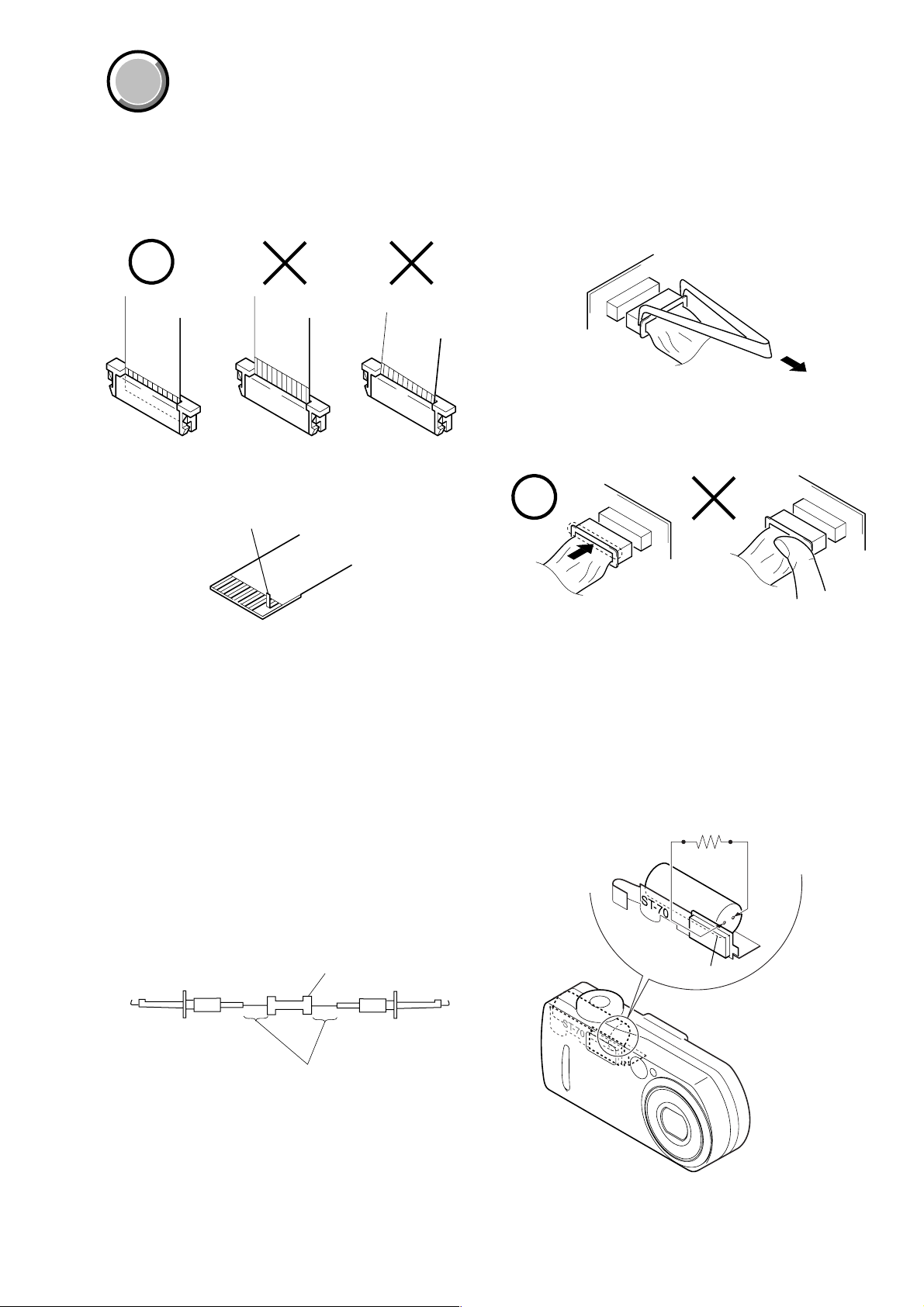
When installing a connector, don’t press down at wire of connector.
It is possible that a wire is snapped.
COVER
COVER
SECTION 1
SERVICE NOTE
• NOTE FOR REPAIR
Make sure that the flat cable and flexible board are not cracked of
bent at the terminal.
Do not insert the cable insufficiently nor crookedly.
Cut and remove the part of gilt
which comes off at the point.
(Be careful or some
pieces of gilt may be left inside)
When remove a connector, don’t pull at wire of connector.
It is possible that a wire is snapped.
[Discharging of the ST-70 flexible board’s charging
capacitor (C003)]
The charging capacitor (C003) of the ST -70 flexible board is char ged
up to the maximum 300 V potential.
There is a danger of electric shock by this high voltage when the
battery is handled by hand. The electric shock is caused by the
charged voltage which is kept without discharging when the main
power of the unit is simply turned off. Therefore, the remaining
voltage must be discharged as described below.
Preparing the Short Jig
To preparing the short jig, a small clip is attached to each end of a
resistor of 1 kΩ /1 W (1-215-869-11).
Wrap insulating tape fully around the leads of the resistor to prevent
electrical shock.
1 kΩ/1 W
Wrap insulating tape.
Discharging the Capacitor
Short-circuit between the positive and the negative terminals of
charged capacitor with the short jig about 10 seconds.
R:1 kΩ/1 W
(Part code:
1-215-869-11)
Capacitor
1-1
Page 6
DSC-P7
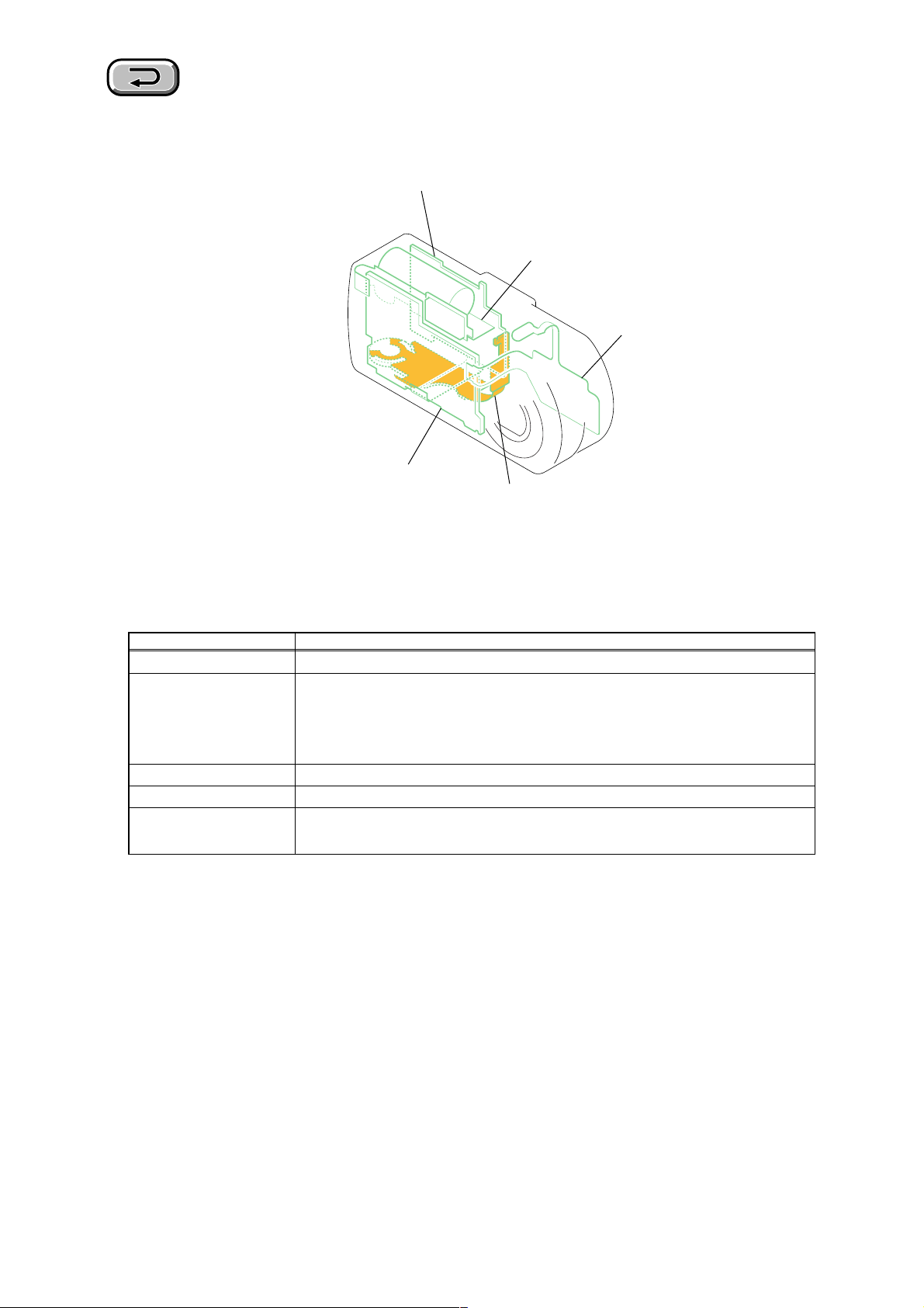
[Precaution on Replacing the Video Lens or the SY-77
Board]
The DSC-P7 uses the position sensor to detect the zoom position.
Accordingly, the zoom position will v ary if the position data changes
due to the replacement of the video lens or the SY-77 board, thus
causing the video lens to collide against the mechanism end when
the power is turned off.
Though the position data is calibrated at the “Flange Back
Adjustment”, add the following work when making an adjustment
at the replacement of video lens to prevent a collision of video lens.
When Replacing the Video Lens
1) With current video lens assembled, turn the power on, and set
the bit value of Bit0 on Page:9, Address:17 to “0” using the
adjusting remote commander, then turn the power off.
2) Replace the video lens with a new one, turn the power on, and
perform the “Flange Back Adjustment”.
Thus, new position data will be written.
3) After the “Flange Back Adjustment”, return the bit value of Bit0
on Page:9, Address:17 to “1” using the adjusting remote
commander.
When Replacing the SY-77 Board
1) Replace the SY-77 board with a new one, set the mode dial to
“PLAY”, turn the power on, and set the bit value of Bit0 on
Page:9, Address:17 to “0” using the adjusting remote
commander, then turn the power off.
2) Set the mode dial to “CAMERA”, turn the power on, and
perform the “Flange Back Adjustment”.
Thus, new position data will be written.
3) After the “Flange Back Adjustment”, return the bit value of Bit0
on Page:9, Address:17 to “1” using the adjusting remote
commander.
[Note in Lens Frame Installation]
When tightening a screw , have both sides of the lens b lock assemb ly
so as not for the load to depend.
M1.7 × 4
Lens block assembly
Lens frame
M1.7 × 4
1-2
Page 7
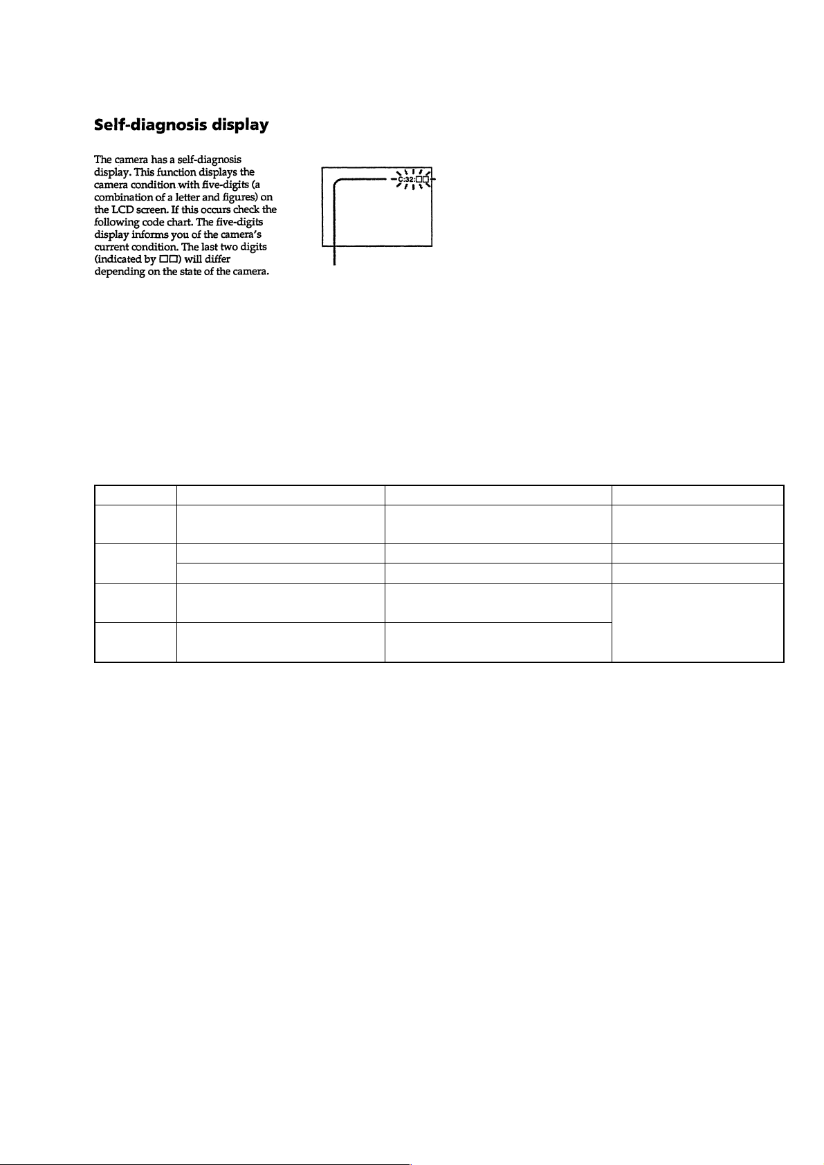
[Description on Self-diagnosis Display]
Self-diagnosis display
• C: ss: ss
You can reverse the camera
malfunction yourself. (However,
contact your Sony dealer or local
authorized Sony service facility
when you cannot recover from the
camera malfunction.)
• E: ss: ss
Contact your Sony dealer or local
authorized Sony service facility.
DSC-P7
Display Code
C:32:ss
C:13:ss
E:61:ss
E:91:ss
Countermeasure
Turn the power off and on again.
Format the “Memory stick”.
Insert a new “Memory Stick”.
Checking of lens drive circuit.
Checking of flash unit or replacement
of flash unit.
Cause
Trouble with hardware.
Unformatted memory stick is inserted.
Memory stick is broken.
When failed in the focus and zoom
initialization.
Abnormality when flash is being
charged.
Caution Display During Error
SYSTEM ERROR
FORMAT ERROR
MEMORY STICK ERROR
—
1-3E
Page 8
DSC-P7
COVER
COVER
SECTION 2
DISASSEMBLY
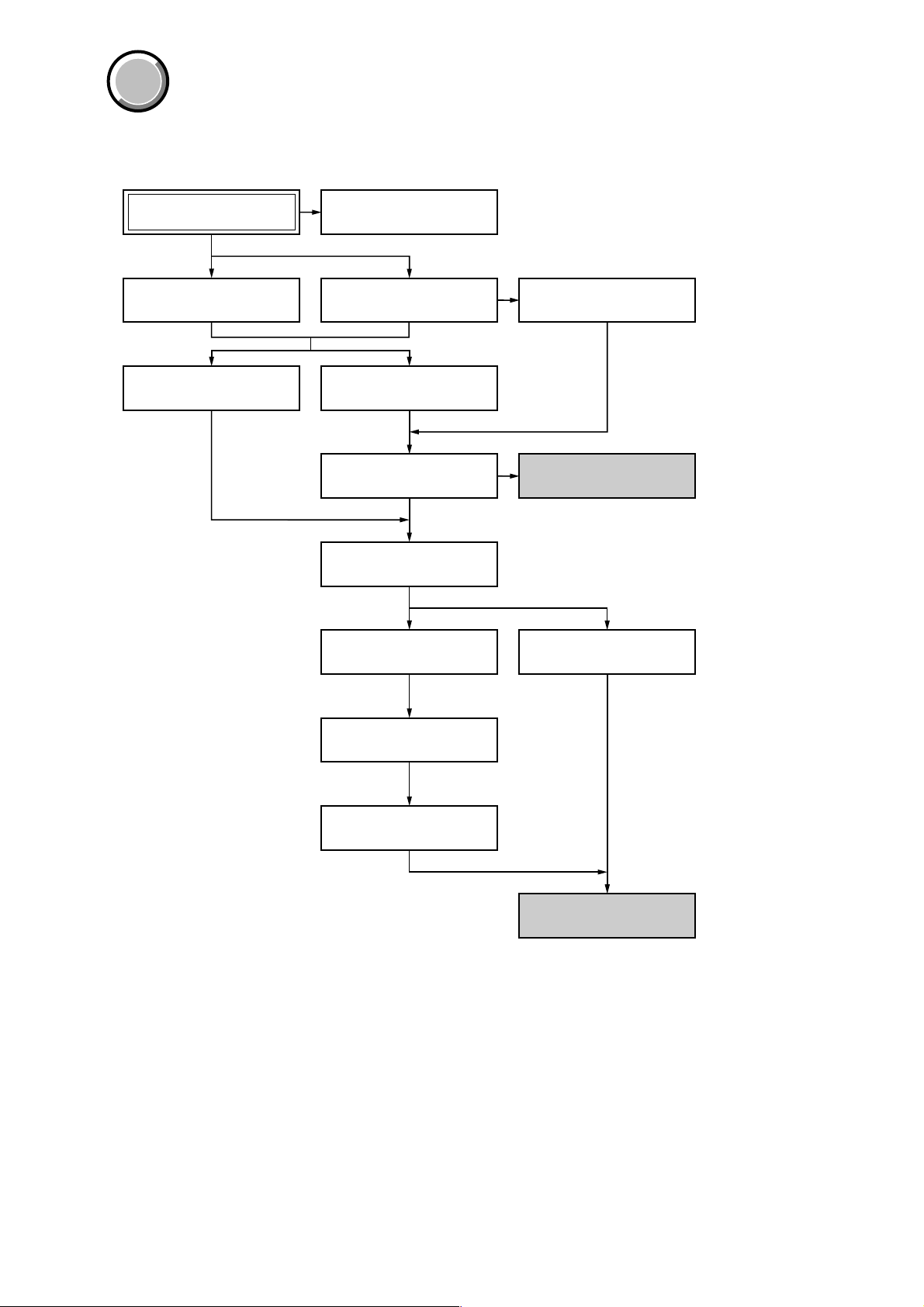
The following flow chart shows the disassembly procedure.
DSC-P7
2-2. CABINET (FRONT)
ASSEMBLY (Page 2-2)
2-7. CONTROL SWITCH
BLOCK (Page 2-5)
2-1. BT LID
(Page 2-2)
2-3. CABINET (REAR)
ASSEMBLY (Page 2-3)
2-5. CABINET (BOTTOM)
ASSEMBLY (Page 2-4)
2-6. LENS BLOCK ASSEMBLY
(Page 2-4)
2-4. LCD MODULE
(Page 2-3)
SERVICE POSITION
(SY-77 BOARD: side A)
(Page 2-5)
2-8. SY-77 BOARD
(Page 2-6)
2-9. MEMORY STICK
CONNECTOR (Page 2-6)
2-11. SW-368 BOARD
(Page 2-7)
2-12. JK-227 BOARD
(Page 2-8)
2-10. ST-70 BOARD
(Page 2-7)
SERVICE POSITION
(SY-77 BOARD: side B)
(Page 2-8)
2-1
Page 9
DSC-P7
Note: Follow the disassembly procedure in the numerical order given.
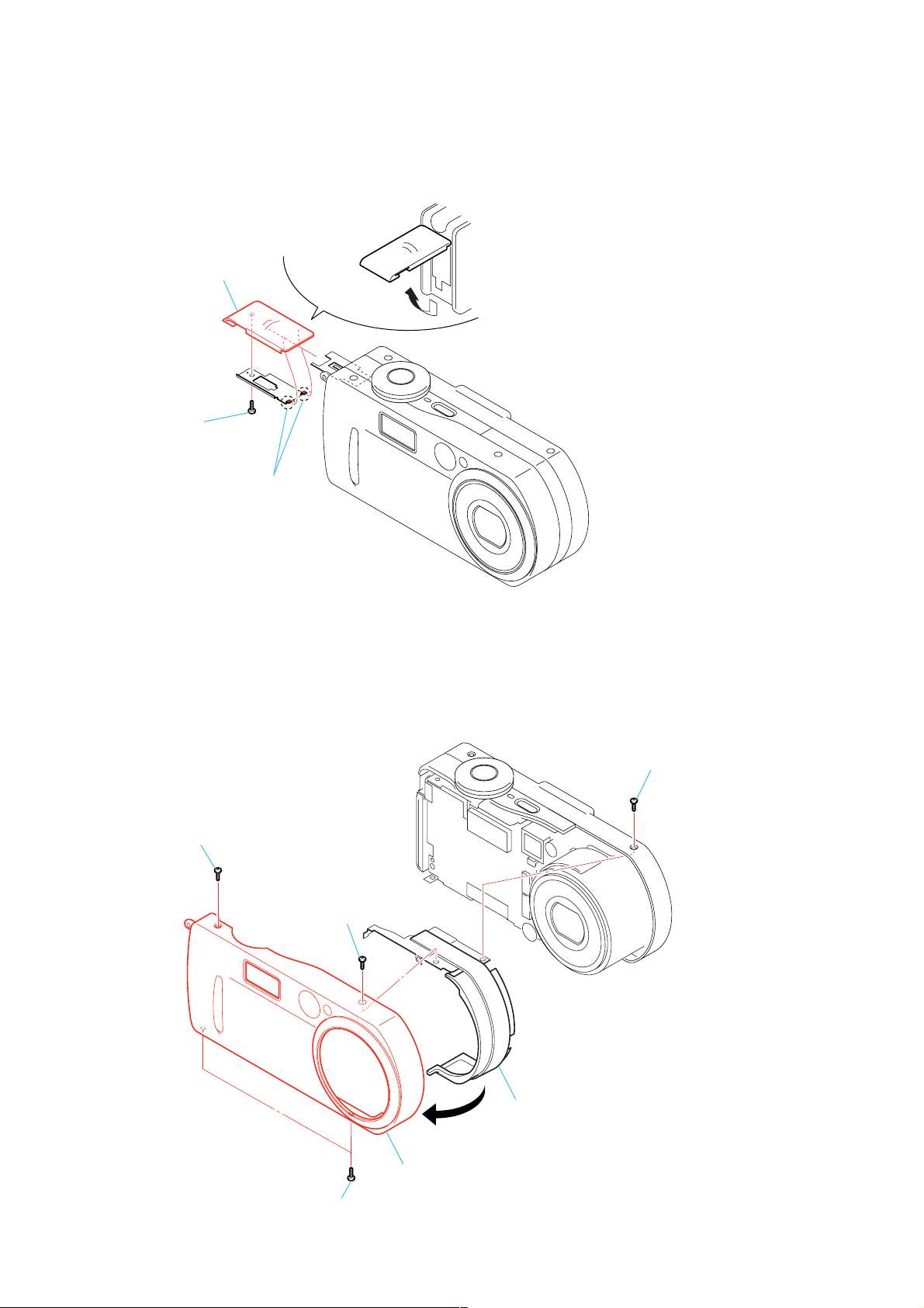
2-1. BT LID
1 Open the BT lid.
4 BT lid
2 Screw
(1.7 × 3)
3 Two claws
2-2. CABINET (FRONT) ASSEMBLY
1 Screw
(M1.7)
2 Screw
(M1.7)
6 Screw
(M1.7)
7 Center cabinet
4
3 Two screws
(M1.7)
5 Cabinet (front)
assembly
2-2
Page 10
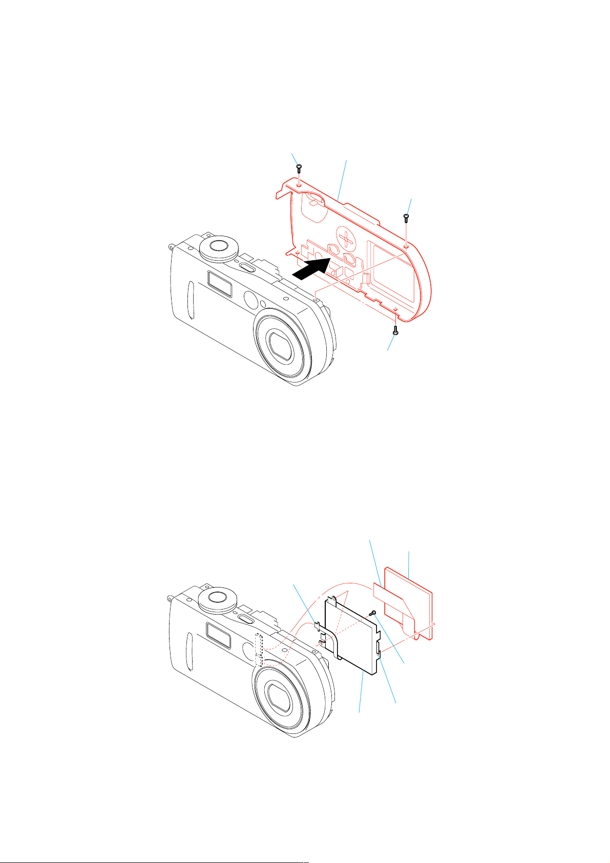
2-3. CABINET (REAR) ASSEMBLY
DSC-P7
2 Screw
(M1.7)
5 Cabinet (rear)
assembly
1 Screw
(M1.7)
4
3 Two screws
(M1.7)
2-4. LCD MODULE
2 Flexible board
(CN102)
6 LCD module
3 Flexible board
(CN101)
1 Two screws
(M1.7)
4 Four claws
5 Back light unit
2-3
Page 11
DSC-P7
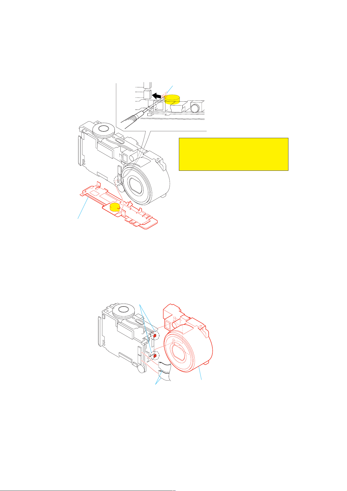
2-5. CABINET (BOTTOM) ASSEMBLY
1 Claw
Rear side
Note: To disengage the claw, pass a flat headed
driver under the flexible cable.
It may be a cause of breakage of the flexible
cable to pass a flat headed driver above the
flexible cable.
2 Cabinet (bottom) assembly
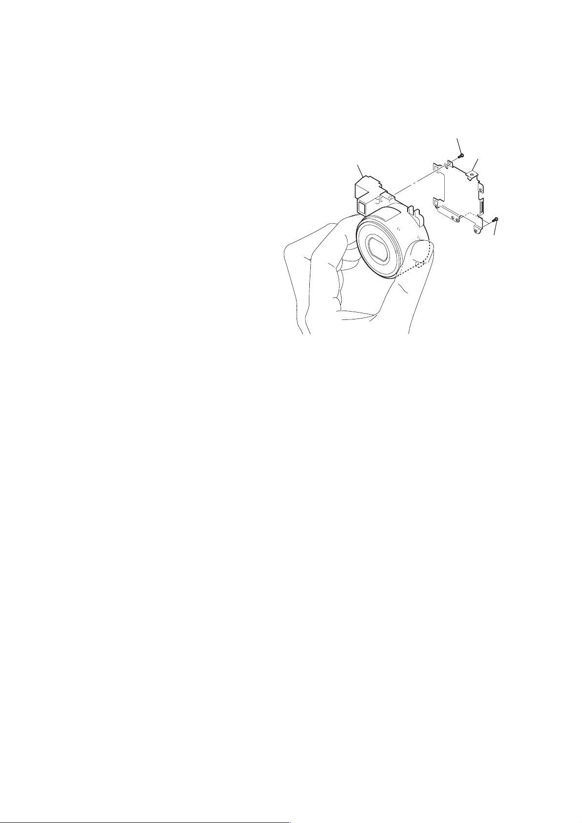
2-6. LENS BLOCK ASSEMBLY
2 Two claws
1 Two flexible board
(CN001, 301)
3 Lens block assembly
2-4
Page 12
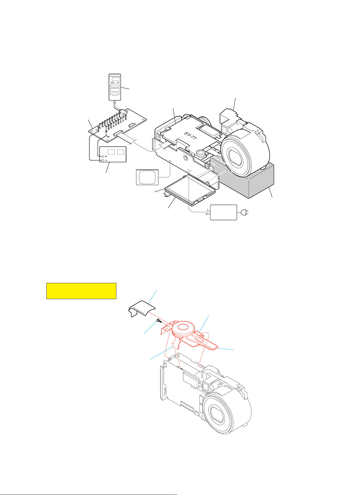
[SERVICE POSITION (SY-77 BOARD: SIDE A)]
DSC-P7
CPC-9 jig
(J-6082-393-C)
Regulated power supply
(6.0 to 7.2 Vdc)
Note 1: Don’t use the 12 pin flexible board of CPC-9 jig.
Note 2: The old CPC-9 jig (Parts code: J-6082-393-B)
Adjusting remote
commander
SY-77 board
18
1
Color monitor
LCD module
Back light unit
18
1
It causes damage to the unit.
cannot be used, because it cannot operate
the adjustment remote commander.
Lens block assembly
Base
AC power
adaptor
AC IN
2-7. CONTROL SWITCH BLOCK
Note: High-voltage cautions
(See page 1-1)
2 Screw
(M1.7)
4 Flexible board
(CN704)
1 Mode dial cover
3 Claw
5 Control swith block
2-5
Page 13
DSC-P7
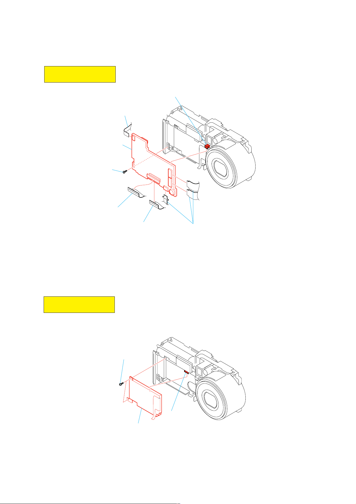
2-8. SY-77 BOARD
Note: High-voltage cautions
(See page 1-1)
5 Claw
1 Connector
(CN351)
7 SY-77 board
4 Screw
(M1.7 × 4)
2 Flexible board
(CN703)
6 Flexible board
2-9. MEMORY STICK CONNECTOR
Note: High-voltage cautions
(See page 1-1)
1 Two screws
(M1.7 × 4)
(CN701)
3 Three flexible boards
(CN001, 301, 702)
2 Claw
3 Memory stick connector
2-6
Page 14
2-10.ST-70 BOARD
1 Connector
(CN351)
3 ST-70 board
DSC-P7
Note: High-voltage cautions
(See page 1-1)
Note: When installing ST-70 board,
the claw is put into the bottom
the BT main frame.
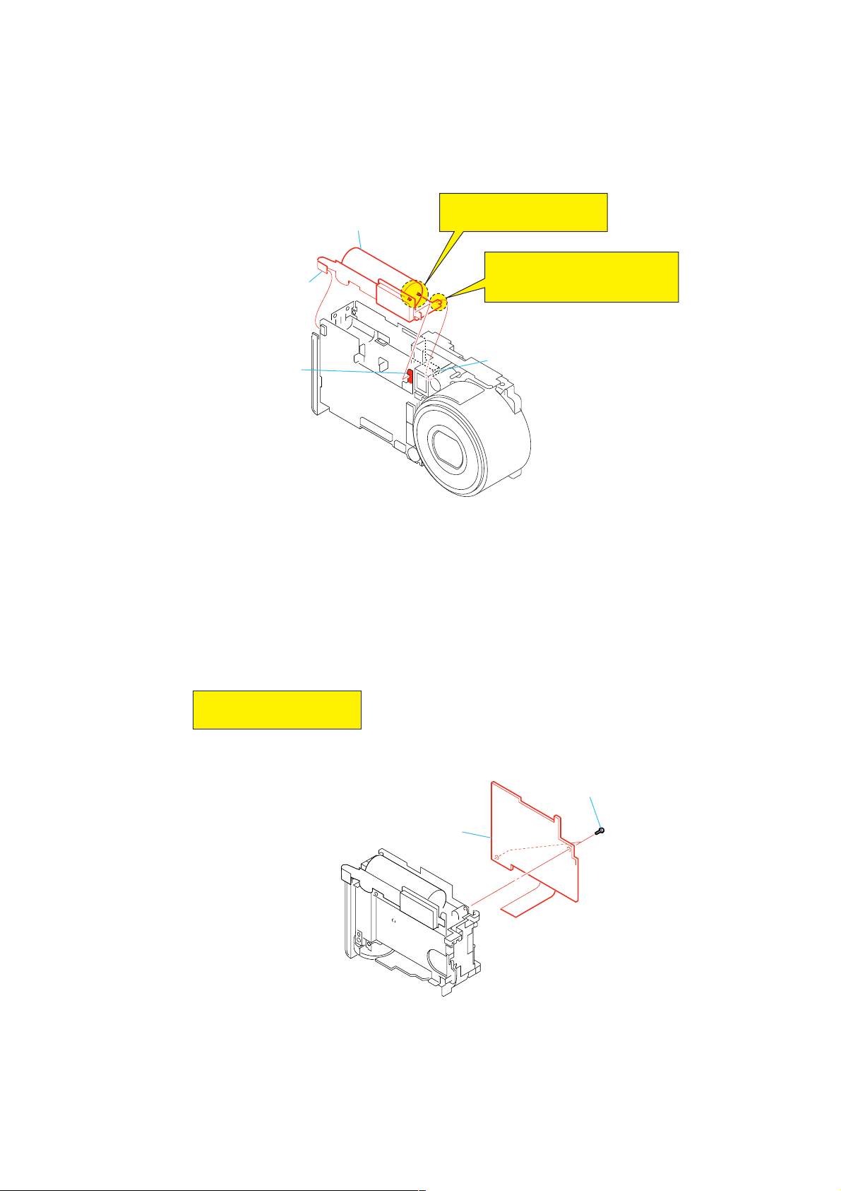
2-11.SW-368 BOARD
Note: High-voltage cautions
(See page 1-1)
2 Claw
BT main frame
2 SW-368 board
2-7
1 Two screws
(M1.7 × 4)
Page 15
DSC-P7
2-12.JK-227 BOARD
Note: High-voltage cautions
(See page 1-1)
6 Claw
2 Claw
7 JK-227 board
(including JK-226)
5 Screw
(M1.7)
3 Claw
4 DD sheet metal
1 Screw
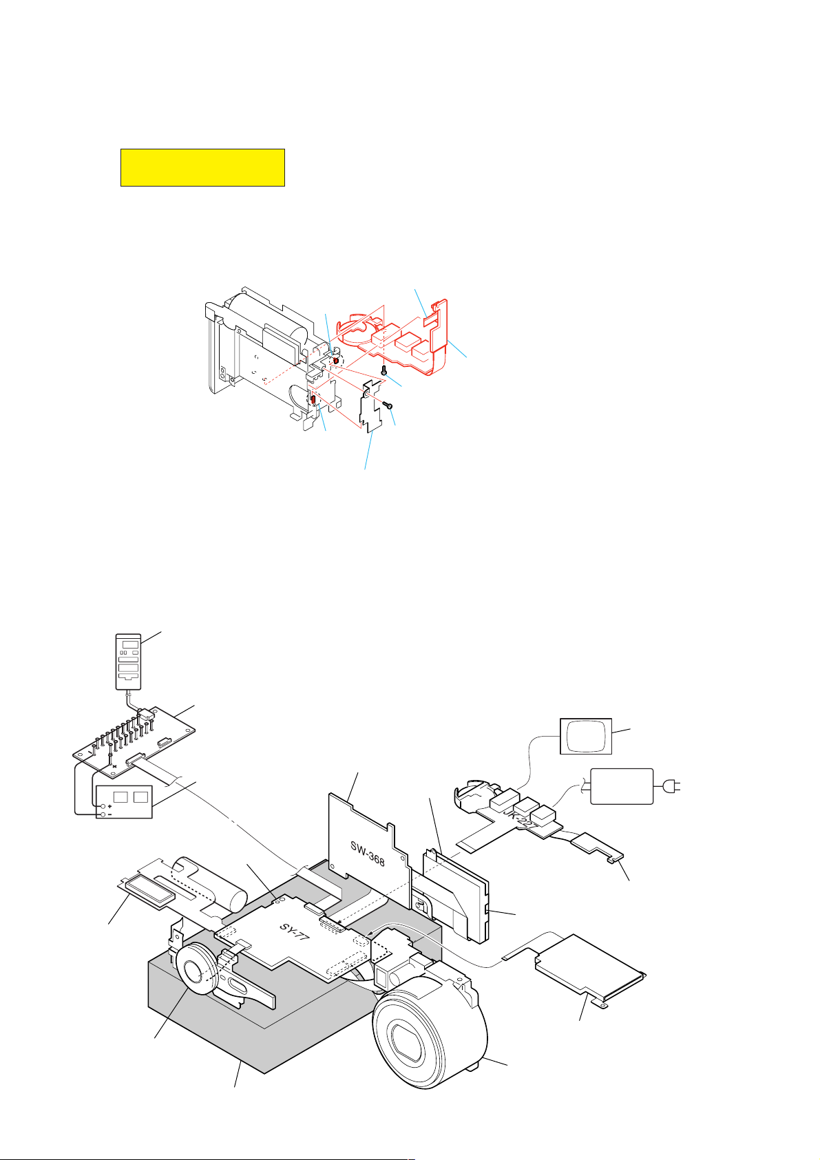
[SERVICE POSITION (SY-77 BOARD: SIDE B)]
Adjusting remote
commander
CPC-9 jig
(J-6082-393-C)
18
1
Regulated power supply
(6.0 to 7.2 Vdc)
Note 1: Don’t use the 12 pin flexible board of CPC-9 jig.
It causes damage to the unit.
Note 2: The old CPC-9 jig (Parts code: J-6082-393-B)
cannot be used, because it cannot operate
the adjustment remote commander.
SW-368 board
LCD module
(M1.7 × 4)
Color monitor
AC power
adaptor
AC IN
ST-70 board
Mode dial block assembly
SY-77 board
Base
18
JK-227 board
1
Back light unit
Memory stick connector
Lens block assembly
2-8
Page 16
2-13.CIRCUIT BOARDS LOCATION
SW-368
SY-77
DSC-P7
ST-70
CD-397
JK-227
(including JK-226)
Board Name Function
CD-397 CCD IMAGER
SY-77 CAMERA MODULE, CAMERA DSP, VIDEO, MEMORY,
LENS DRIVE, SH DSP, FLASH MEMORY, FRONT CONTROL,
AUDIO, CLOCK GENERATOR, FLASH CONTROL,
DC/DC CONVERTER, CAMERA PROCESS
ST-70 FLASH DRIVE
SW-368 CONTROL SWITCH, LCD DRIVE, TIMING GENERATOR
JK-227 JACK
(including JK-226)
2-9E
Page 17
COVER
COVER
3. BLOCK DIAGRAMS
Link
Link
OVERALL BLOCK DIAGRAM POWER BLOCK DIAGRAM 2
OVERALL BLOCK DIAGRAM POWER BLOCK DIAGRAM 2
POWER BLOCK DIAGRAM 1
POWER BLOCK DIAGRAM 1
DSC-P7
Page 18

DSC-P7
COVER
COVER
BLOCK DIAGRAMS
3-1. OVERALL BLOCK DIAGRAM
LENS
TEMP
SENSOR
SHUTTER
MOTOR
LENS
ZOOM
MOTOR
MM
ZOOM
POSITION
SENSOR
SENSOR
CD-397 BOARD (2/2)
D101
SELF TIMER/
AF ILLUMINATOR
ZOOM
FOCUS
MOTOR
M
FOCUS
SENSOR
IRIS
MOTOR
IRIS
METER
M
SECTION 3
3. BLOCK DIAGRAMS
3. BLOCK DIAGRAMS
( ) : Number in parenthesis ( ) indicates the division number of schematic diagram where the component is located.
CCD OUT
SY-77 BOARD
IC151
CAMERA
MODULE
(1/10)
(D/A CONVERTER)
ZOOM POS
LENS TEMP
SELF TIMER LED
DATA BUS 14
IC508
EVR
(6/10)
HR DIR0A, HR DIR0B, HR EN0
HR DIR1A, HR DIR1B, HR EN1
IRIS M IN, IRIS M EN,
IRIS S IN, IRIS S EN
MSHUT ON
MSHUT EN
XFC RST SENS
XZM RST SENS
STRB ON
CAM SO, XCAM SCK
IC601
CAMERA
DSP
(2/10)
PANEL R
PANEL G
PANEL B
CV OUT
ADDRESS BUS14
DATA BUS 32
25
16
ADDRESS BUS
AU AINL
AU AOUT
25
16
20
DATA BUS
16
IC602
128M
SDRAM
(3/10)
IC504
16M FLASH
(6/10)
ZOOM POS
LENS TEMP
IC501
MC CAM,
SH DSP
(5/10)
BEEP, BEEP ON
CD-397 BOARD (1/2)
IC302
(4/10)
FOCUS MOTOR
DRIVER
ZOOM MOTOR
DRIVER
IRIS
DRIVER
SHUTTER DRIVER
IC101
CCD IMAGER
V1A, V1B, V2
V3A, V3B, V4
VSUB CONT
H1, H2
PRELAMP AF ON
CAM SO, XCAM SCK
SP VOL
AU AINL
AU AOUT
IC505
EEPROM
(6/10)
VAMP ON
USB D+
USB D
LCD SO, XLCD SCK
CV OUT
−
IC201
AUDIO AMP
(8/10)
MS DIO, MS BS, MS SCLK
IC101
VIDEO AMP
(3/10)
SW-368 BOARD (1/2)
PANEL R
PANEL G
PANEL B
LCD SO, XLCD SCK
V OUT
AU OUT
MS
SOCKET
JK-226 BOARD (2/2)JK-227 BOARD (2/2)
IC101
LCD DRIVE
(2/2)
IC102
LCD TIMING
GENERATOR
(2/2)
USB D+
USB D–
SP901
SPEAKER
PANEL UNIT
VR
VG
VB
CN002
USB
LCD901
COLOR
LCD
MONITOR
D901
BACK LIGHT
J002
A/V OUT
(MONO)
FLASH
UNIT
ST-70 BOARD (1/2)
CHARGING
CAPACITOR
Q002
J001
DC IN
JK-226 BOARD (1/2)
T001
BT901
BATTERY
TERMINAL
JK-227 BOARD (1/2)
+
S
–
Q360, 361
ACV UNREG
STB CHARGE
XSTB FULL
X501
27MHz
IC507
CLOCK GEN.
(6/10)
IC001
DC/DC
CONTROL
(10/10)
TG CLK
USB CLK
MC CLK
CAM 15V
CAM 3.2V
CAM –7.5V
A 4.9V
A 2.9V
D 1.5V
D 2.9V
PANEL 2.9V
BL VO–
FR 5V
AVC UNREG
BATT UNREG
UNREG SCK, UNREG SO
BEEP, BEEP ON
SELF TIMER LED
STB CHG
XSTB FULL
SYS DD ON
BATT SIG
IC401
FRONT CONTROLLER
(7/10)
RESET
KEY AD0, 1
KEY AD3
MODE DIAL, XPB ON, XSET UP ON
XPWR ON
XAE LOCK SW, XSHTR ON
IC403
INITIAL RESET,
BACK UP VCC
(7/10)
MIC901
MICROPHONE
ST-70 BOARD (2/2)
BT001
LITHIUM
FR 5VEVER 3.0V
BATTERY
SW-368 BOARD (2/2)
FUNCTION
SWITCH
ZOOM
SWITCH
CONTROL SWITCH BLOCK
MODE
DIAL
POWER
ON/OFF
SHUTTER
SWITCH
05
3-1 3-2
Page 19

Any block diagrams except for the overall block diagram
and the power block diagram are not shown.
Pages from 3-3 to 3-14 are not shown.
Page 20

DSC-P7
COVER
COVER
3. BLOCK DIAGRAMS
3. BLOCK DIAGRAMS
3-8. POWER BLOCK DIAGRAM 1
SY-77 BOARD (1/2)
CN703
17
ı
24
37
1
ı
8
36
9
ı
16
CN351
4
ST UNREG
ı
8
VL 3V
1
J001
DC IN
BT901
BATTERY
TERMINAL
JK-226 BOARD
ACV UNREG
BATT/XEXT
BATT UNREG1
+
BATT SIG
S
BATT GND
–
FLASH
UNIT
GND
ST-70 BOARD
BT001
LITHIUM
BATTERY
JK-227 BOARD
ACV UNREG1
BATT/XEXT
BATT
UNREG1
BATT SIG
GND
T001
( ) : Number in parenthesis ( ) indicates the division number of schematic diagram where the component is located.
F004
Q017, 018
Q015, 021
CHARGE
CONTROL
Q360, 361
FAST CHARGE
INIT CHARGE
D008
F001
BATT/XEXT
BATT SIG
L351
STB CHARGE
F003
FAST CHARGE
INIT CHARGE
BATT/EXT
BATT SIG
D009
D007 D001
D006
Q408
BATTERY
CHARGE
DETECTOR
L016
FR 5V
DD CON SENS
D407
IC403
INITIAL RESET,
BACK UP VCC
(7/10)
IC404
FRONT CONTROLLER
(7/10)
66 DD CON SENS
68
ACV SENS
67 BATT SENS
48
FAST CHARGE
INIT CHARGE
47
8
BATT/XEXT
BATT SI
43
BATT SO
42
46 STB CHG
SYS DD ON
XCS DDCON
UNREG SO
UNREG SCK
IC002
(10/10)
DC/DC
CONVERTER
L401
76
XCS DDCON
22
20
UNREG SCK
21
EVER 3.0V
SYS DD ON
UNREG SO
L017
DC/DC CONTROL
47
RST
48
LD ON
56
VCC1
57
CONT
44
XCS
45
DATA
46
CLK
D010
IC001
(10/10)
AMP OUT
VCC2
OUT 1p
OUT 1n
VIN 1–
OUT 4p
OUT 4n
VIN 4–
VCC3
VCC5
OUT 5p
OUT 5n
OUT 5S
VIN 5–
OUT 6p
OUT 6n
OUT 6S
VIN 6–
VCC4
OUT 9
IN 9–
SCP 9
OUT 10
AMP IN
IN 10
SCPIN
41
36
37
55
30
31
53
42
20
38
39
43
52
28
29
18
50
19
23
80
1
22
4
5
−
3
10
L004
L002
SWITCHING
Q008, 010
SWITCHING
Q009, 011
SWITCHING
EMERGENCY
Q002, 005
Q001
DETECT
L005L019 L011
Q003, 006
L020
SWITCHING
Q012
Q013
Q004
SWITCHING
L006
L012
L013
L001
D004 D005
Q007
SWITCHING
L010
L007
L008
L009
L021
D002 D013
CN706
HI UNREG
CN704
PWR LED VCC
D 2.9V
IC003
(10/10)
3.2V
REG
L014
Q019, 020
–7.5V
REG
CPC
10
(FOR CHECK)
CONTROL SWITCH BLOCK
12
3
EVER 3.0V
D 1.5V
D 2.9V
A 2.9V
PANEL 2.9V
A 4.9V
CAM 3.2V
M 5V
CAM 15V
BL VO–
CAM –7.5V
D 2.9V
A
(POWER)
POWER 2
(PAGE 3-17)
05
3-15 3-16
Page 21

COVER
COVER
3. BLOCK DIAGRAMS
3. BLOCK DIAGRAMS
DSC-P7
3-9. POWER BLOCK DIAGRAM 2
SY-77 BOARD (2/2)
POWER 1
(PAGE 3-16)
PANEL 2.9V
EVER 3.0V
BL VO–
CAM 15V
CAM −7.5V
A
A 4.9V
M 5V
CAM 3.2V
D 2.9V
D 1.5V
CN701
( ) : Number in parenthesis ( ) indicates the division number of schematic diagram where the component is located.
SW-368 BOARD
CAM15V
32
33
PANEL 2.9V
11
12
EVER 3.0V
3
A 4.9V
30
31
BL VO–
1
2
Q002, 003
13.5V
REG
D003
(AE LOCK)
D004
(TALLY)
D002
(FLASH/CHG)
L102
L101
L104
L503
LCD DRIVER
LCD TIMING
GENERATOR
IC508
EVR
(D/A CONV.)
(6/10)
IC101
(2/2)
IC102
(2/2)
XP OFF
Q105, 108
14
CAM 15V
CAM −7.5V
A 4.9V
M 5V
CAM 3.2V
D 2.9V
D 1.5V
IC103
BACK LIGHT
CONTROL
(2/2)
IC505
EEPROM
(6/10)
Q108
REF VOLTAGE
GEN
CN102
18
D102
16
11
CN101
IC507
CLOCK GEN.
(6/10)
9
6
1
VDD
VDDG
CRext
REF
BL THH
BL L
PANEL UNIT
MONITOR
BACK LIGHT
Q152 - 153
FB506FB504
LCD901
COLOR
LCD
D901
CAM DD ON
IC504
16M FLASH
(6/10)
FB155
FB154
MS POWER ON
L504
FB501
FB502
L501
L152
L153
L154
L101
FB151
FB153
FB152
198
PTM (6)
30
D32/PTA (7)
IC501
MC CAM, SH DSP
(5/10)
IC101
CAMERA
MODULE
(1/10)
CAM 15V
CAM −7.5V
D702
(MS ACCESS)
Q701
CN001
M 5V
CN702
CD-397 BOARD
6
FB101
7
24
VCC
MEMORY
2
6
STICK
IC101
CCD IMAGER
D101
SELF TIMER/
AF ILLUMINATOR
LENS BLOCK
CN301
Q301
19
11
14
F RST VCC
Z RST VCC
Z POSI VCC
ZOOM
ZOOM
SENSOR
SENSOR
FOCUS
SENSOR
ZOOM
POSITION
SENSOR
IC101
(3/10)
L303
L302
L301
Q302
IC302
7CH LENS DRIVER
(4/10)
IC301
BUFFER
(4/10)
D 2.9V
A 2.9V
L203
L201
L202
L602
FB601
L601
FB602
05
IC601
CAMERA DSP
(2/10)
A 2.9V
M 5V
IC201
AUDIO AMP
(8/10)
FB603
IC602
128M
SDRAM
(3/10)
L101
VIDEO AMP
3-17 3-18E
Page 22

COVER
COVER
PRINTED WIRING BOARDS AND SCHEMATIC DIAGRAMS
4-1. FRAME SCHEMATIC DIAGRAMS
SECTION 4
4-2. SCHEMATIC DIAGRAMS 4-3. PRINTED WIRING BOARDS
4-2. SCHEMATIC DIAGRAMS 4-3. PRINTED WIRING BOARDS
DSC-P7
1
23
4 138
712
9
10
1165
FRAME (1/2)
A
2
1
8
XPB_ON
CONTROL
SWITCH
BLOCK
(POWER (GREEN))
5
6
7
NC
NC
GND
S004
POWER
D001
3
4
D_2.9V
MODE_DIAL
1
2
XSHTR_SW
XAE_LOCK_SW
PANEL UNIT
B
D901
BACK
LIGHT
LCD901
1.5INCH
COLOR
B
G
6
A
S005
MODE DIAL
LCD UNIT
1
3
S003
(SHUTTER)
2
4
C
123
4
5
6
BL_THH
CN101 6P
11
12
13
14CS15
16
17
18
19
20EN21
22
23
24
NC
BL_THL
BL_H
NC
BL_L
TEST
COM
VST
VCK
DWN
VDD
VSS
VSSG
VDDG
WIDE
REF
HST
10
SDUT
9
CRext
7
PSIG
HCK18HCK2
D
1
2
3B4R5G6
RGT
TEST2
CN102 24P
MIC901
MICROPHONE
CN705 2P
1
MIC_SIG
2
REG_GND
14
XPWR_ON
CN704 14P
13
NC
10
11
12
XSET_UP
XPWR_LED
PWR_LED_VCC
9
XMOVIE
CN701 33P
1
BL_VO-
2
E
SW-368 BOARD
F
(STROBO/CHARGE_LED (YELLOW))
G
H
D002
D003
(AE_LOCK (GREEN))
D004
(TALLY (RED))
S004
CONTROL
MENU DISPLAY
S005S003
ZOOM
S001 S002
TW
3
4
5
6
7
8
9
10
11
12
13
14
15
16
17
18
19
20
21
22
23
24
25
26
27
28
29
30
31
32
33
BL_VO-
EVER_3.0V
KEY_AD0
AE_LOCK_LED
KEY_AD1
XCHARGE_LED
PANEL_HDD
XTALLY_LED
HDO
PANEL_2.9V
PANEL_2.9V
PANEL_V
LCD_SO
KEY_AD3
XCS_PANEL_TG
XLCD_SCK
REG_GND
REG_GND
REG_GND
REG_GND
REG_GND
PANEL_R
PANEL_G
PANEL_B
REG_GND
PANEL_COM
PANEL_VG
XRST_SYS
A_4.9V
A_4.9V
CAM_15V
CAM_15V
SY-77 BOARD (1/2)
D702
(MS ACCESS LED (RED))
S401
RESET
I
HSY
CPC_IN
N.C
N.C
REG_GND
N.C
05
CN706 18P
123456789
PANEL_COM
N.C
LANC_OUT
HI_UNREG
VG
LANC_IN
101112131415161718
N.C
N.C
N.C
N.C
N.C
N.C
4-1 4-2
CPC
(FOR CHECK)
FRAME (1/2)
Page 23

DSC-P7
COVER
COVER
4-2. SCHEMATIC DIAGRAMS 4-3. PRINTED WIRING BOARDS
4-2. SCHEMATIC DIAGRAMS 4-3. PRINTED WIRING BOARDS
1
FRAME (2/2)
A
B
C
D
E
F
G
H
23
ST-70 BOARD
FLASH
C003
CHARGING
CAPACITOR
+
BT001
LITHIUM BATTERY
(BACK UP)
4 138
CN351 15P
VL_3V
1
2
STB_ON1
3
STB_FULL
ST_UNREG
4
ST_UNREG
5
ST_UNREG
6
ST_UNREG
7
ST_UNREG
8
REG_GND
9
REG_GND
10
REG_GND
11
REG_GND
12
REG_GND
13
REG_GND
14
REG_GND
15
ACV_UNREG1
SP+
BATT/XEXT
USB_JACK_IN
SP-
CN703 39P
3938373635343332313029282726252423222120191817161514131211
AV_JACK_IN
AU_OUT
N.C.
USB_DATA+
V_OUT
USB_DATA-
BATT SIG
USB_GND
USB_GND
AV_GND
AV_GND
ACV_UNREG1
ACV_UNREG1
ACV_UNREG1
ACV_UNREG1
ACV_UNREG1
ACV_UNREG1
ACV_UNREG1
JK-227 BOARD
SY-77 BOARD (2/2)
GND
GND
GND
GND
GND
GND
GND
BATT_UNREG1
GND
987654321
10
BATT_UNREG1
BATT_UNREG1
BATT_UNREG1
BATT_UNREG1
BATT_UNREG1
BATT_UNREG1
BATT_UNREG1
9
CN702 8P
10 14
SCLK
INT
VCC
FP-478
FLEXIBLE
BOARD
DIO
VCC
VSS
1234567
1165
CN001 25P
PRE_LAMP
CCD_TEMP_AD
VSUB_CONT
CN301 27P
F_RST_VCC
F_RST_GND
F_RST_SENS
Z_POSI_OUT
Z_POSI_GND
Z_POSI_VCC
TEMP_OUT
TEMP_GND
Z_RST_VCC
Z_RST_SENS
Z_RST_GND
BS
VSS
8
CCD_OUT
VSHUT
CAM_-7.5V
CAM_15V
ZOOM_A
ZOOM_A
ZOOM_B
ZOOM_B
FOCUS_A
FOCUS_B
FOCUS_A
FOCUS_B
IRIS_S-
IRIS_S+
IRIS_M-
IRIS_M+
SHUTTER-
SHUTTER-
SHUTTER+
SUTTEER+
M_5V
25
24
23
GND
22
GND
21
GND
20
19
GND
18
GND
V4
V3A
V3B
V1B
V1A
V2
GND
GND
H1
RG
H2
GND
D101
SELF TIMER/
17
AF ILLUMINATOR
16
15
14
13
12
CD-397 BOARD
11
10
9
8
7
6
5
4
3
2
1
27
26
25
24
23
22
21
20
19
18
17
16
15
14
13
12
11
10
9
8
7
6
5
4
3
2
1
LENZ UNIT
LENZ
CCD
OPTICAL
VIEW
FINDER
15712
I
J
05
FRAME (2/2)
SP901
SPEAKER
USB
JK-226 BOARD
MS
SOCKET
A/V OUT
(MONO)
J002
GND
CN002 5P
5
BT901
DC IN
VCC2D-3D+
4ID
1
J001
BATTERY
TERMINAL
4-3 4-4
Page 24

4-2. SCHEMATIC DIAGRAMS
COVER
COVER
4-2. SCHEMATIC DIAGRAMS
4-2. SCHEMATIC DIAGRAMS
THIS NOTE IS COMMON FOR SCHEMATIC DIAGRAMS
(In addition to this, the necessary note is printed in each block)
DSC-P7
(For schematic diagrams)
• All capacitors are in µF unless otherwise noted. pF : µ
Link
µF. 50 V or less are not indicated e xcept for electrolytics
and tantalums.
• Chip resistors are 1/10 W unless otherwise noted.
kΩ=1000 Ω, MΩ=1000 kΩ.
• Caution when replacing chip parts.
New parts must be attached after removal of chip.
Be careful not to heat the minus side of tantalum
capacitor, Because it is damaged by the heat.
• Some chip part will be indicated as follows.
Example C541 L452
22U 10UH
TA A 2520
Kinds of capacitor
Temperature characteristics
External dimensions (mm)
• Constants of resistors, capacitors, ICs and etc with XX
indicate that they are not used.
In such cases, the unused circuits may be indicated.
• Parts with ★ differ according to the model/destination.
Refer to the mount table for each function.
• All variable and adjustable resistors have characteristic
curve B, unless otherwise noted.
• Signal name
XEDIT→ EDIT PB/XREC → PB/REC
• 2: non flammable resistor
• 5: fusible resistor
• C: panel designation
• A: B+ Line
• B: B– Line
• J : IN/OUT direction of (+,–) B LINE.
• C: adjustment for repair.
• A: VIDEO SIGNAL (ANALOG)
• A: AUDIO SIGNAL (ANALOG)
• A: VIDEO/AUDIO SIGNAL
• A: VIDEO/AUDIO/SER V O SIGNAL
• A: SERVO SIGNAL
• Circled numbers refer to waveforms.
(Measuring conditions voltage and waveform)
• Voltages and waveforms are measured between the
measurement points and ground when camera shoots
color bar chart of pattern box. They are reference values
and reference waveforms.
(VOM of DC 10 MΩ input impedance is used)
• Voltage values change depending upon input
impedance of VOM used.)
1. Connection
Pattern box
L
Front of the lens
L = About 25 cm
2. Adjust the distance so that the output waveform of
Fig. a and the Fig. b can be obtain.
H
Yellow
Cyan
White
Magenta
Green
AABBA=B
Fig. a (Video output terminal output waveform)
Fig.b (Picture on monitor TV)
When indicating parts by reference number, please
include the board name.
Red
Blue
Note : The components identified by mark 0 or
dotted line with mark 0 are critical for safety.
Replace only with part number specified.
Note : Les composants identifiés par une marque
0 sont critiques pour la sécurité.
Ne les remplacer que par une pièce portant
le numéro spécifie.
4-5
Page 25

COVER
COVER
Link
Link
DSC-P7
4-2. SCHEMATIC DIAGRAMS
CD-397 BOARD
CD-397 BOARD
SW-368 BOARD (1/2) (CONTROL SWITCH)
SW-368 BOARD (1/2) (CONTROL SWITCH)
SW-368 BOARD (2/2)
SW-368 BOARD (2/2)
(LCD DRIVE, TIMING GENERATOR)
(LCD DRIVE, TIMING GENERATOR)
COMMON NOTE FOR SCHEMATIC DIAGRAMS WAVEFORMS
COMMON NOTE FOR SCHEMATIC DIAGRAMS WAVEFORMS
(CCD IMAGER)
(CCD IMAGER)
ST-70 BOARD (FLASH DRIVE)
ST-70 BOARD (FLASH DRIVE)
CONTROL SWITCH BLOCK
CONTROL SWITCH BLOCK
Page 26

COVER
COVER
For Schematic Diagram
• Refer to page 4-41 for printed wiring board.
4-2. SCHEMATIC DIAGRAMS CD-397 PRINTED WIRING BOARD
4-2. SCHEMATIC DIAGRAMS CD-397 PRINTED WIRING BOARD
DSC-P7
1
2
CD-397 BOARD
A
B
C
D
E
F
CCD IMAGER(CCD BLOCK)
XX MARK:NO MOUNT
LND125
LND124
LND123
LND122
LND121
LND120
LND119
LND118
LND117
LND116
LND115
LND114
LND113
LND112
LND111
LND110
LND109
LND108
LND107
LND106
LND105
LND104
LND103
LND102
LND101
SIGNAL PATH
REC
05
SY-77 (1/10)
CN001
( PAGE 4-9)
25
PRE_LAMP
24
23
CCD_GND
22
CCD_GND
21
CCD_GND
20
CCD_OUT
19
CCD_GND
18
CCD_GND
17
16
15
14
13
12
11
CCD_TEMP
10
9
VSUB_CONT
8
7
CAM_-7.5V
6
CAM_15V
5
4
3
2
1
Y/CHROMA
M_5V
V4
V3A
V3B
V1B
V1A
V2
VSHUT
GND
GND
H1
RG
H2
GND
VIDEO
SIGNAL
3
D101
OPR5052
SELF TIMER/
AF ILLUMINATOR
TH101
4
Note: voltage and waveform of mounted on CD-397 board
can not be measured, because they are (mounted)
by the side of the lens.
R101
0
(CCD TEMP SENSOR)
R103
0
100
R102
R104
0
R109
XX
FB101
C101
Q101
2SC4250(T5LSONY1)
BUFFER
C102
XX
R105
3300
0.1u
C104
10u
16V
C103
0.1u
16V
C105
7
C106
0.1u
16V
10p
R108
10k
1V42
V3A3V3B
IC101
ICX406AQF-13
IC101
C109
0.1u
7
8
9
10
GND
TEST
TEST
VOUT
VDD12RG13H214H115GND16VSHT17CSUB18VL19H120H2
11
R107
1M
C108
2200p
C107
0.1u
DTC144EHT2L
4V25
V1A6V1B
22
R106
Q102
SWITCH
865
CCD IMAGER
Precautions for Replacement of CCD Imager
• The CD-397 board mounted as a repair part is not equipped
with a CCD imager.
When replacing this board, remove the CCD imager from the
old one and mount it onto the new one.
• If the CCD imager has been replaced, carry out all the
adjustments for the camera section.
• As the CCD imager may be damaged by static electricity from
its structure, handle it carefully like for the MOS IC.
In addition, ensure that the receiver is not covered with dusts
nor exposed to strong light.
4-7 4-8
CD-397
Page 27

Schematic diagram of the SY-77 board are not shown.
Pages from 4-9 to 4-28 are not shown.
Page 28

DSC-P7
COVER
COVER
4-2. SCHEMATIC DIAGRAMS SW-368 PRINTED WIRING BOARD
4-2. SCHEMATIC DIAGRAMS SW-368 PRINTED WIRING BOARD
For Schematic Diagram
• Refer to page 4-47 for printed wiring board.
1
3
5
9116842
107
SW-368 BOARD (1/2)
A
CONTROL SWITCH(KEY BLOCK)
XX MARK:NO MOUNT
NO MARK:REC/PB MODE
CL001
BL_VO-
CL002
BL_VO-
CL003
EVER_3.0V
CL004
KEY_AD0
KEY_AD1
PANEL_V
LCD_SO
KEY_AD3
XLCD_SCK
REG_GND
REG_GND
REG_GND
REG_GND
REG_GND
PANEL_R
PANEL_G
PANEL_B
REG_GND
PANEL_VG
XRST_SYS
A_4.9V
A_4.9V
CAM_15V
CAM_15V
HDO
CL005
CL006
CL007
CL008
CL009
CL010
CL011
CL012
CL013
CL014
CL015
CL016
CL017
CL018
CL019
CL020
CL021
CL022
CL023
CL024
CL025
CL026
CL027
CL028
CL029
CL030
CL031
CL032
CL033
B
AE_LOCK_LED
XCHARGE_LED
PANEL_HDO
XTALLY_LED
PANEL_2.9V
PANEL_2.9V
C
SY-77 (6/10)
CN701
(SEE PAGE 4-20)
XCS_PANEL_TG
D
PANEL_COM
E
F
SIGNAL PATH
VIDEO SIGNAL
CHROMA
REC
G
PB
H
I
BL_VO-
BL_VO-
PANEL_HDO
PANEL_V
LCD_SO
XCS_PANEL_TG
XLCD_SCK
PANEL_R
PANEL_G
PANEL_B
PANEL_COM
PANEL_VG
XRST_SYS
A_4.9V
A_4.9V
HDO
R012
1200
LEFT
13.4
R009
820
R008
330
R007
560
LND001
STATIC_GND
D004
TALLY(RED)
D003
AE_LOCK(GREEN)
STROBO/CHARGE_LED(YELLOW)
D002
(YELLOW)
W
W ZOOM T
R010
1200
R011
1500
B1
T
S002S001
PANEL_R
PANEL_G
PANEL_B
XRST_SYS
HDO
PANEL_V
LCD_SO
XLCD_SCK
XCS_PANEL_TG
A_4.9V
BL_VO-
PANEL_HDO
PANEL_VG
PANEL_COM
B2
R018
470
2.2
0
Q004
UN9213J-(K8).SO
LED DRIVE
D001
MAZT082H08S0
D006
C002
0.22u
MAZT082H08S0
R002
33k
0.5%
R003
240k
0.5%
13.3
D005
MAZT082H08S0
R005
100k
14.1
2
14
12.9
R006
100k
15.2
36
HN1C01FU-TE85R
D004
CL-196HR-CD-T
D003
CL-196YG-CD-T
D002
SML-310YTT86
MAZT082H08S0
Q003
HN1A01FU-TE85R
B+ SWITCH
14.5
2
1
4
14.1
5
13.4
5
Q002
B+ SWITCH
D007
R004
XX
6
3
S004
CONTROL
1200
RIGHT
SET
DOWN
B1
2
4
B2
DISPLAY
S005
R015
1500
R014
3300
A1
1
3
A2
(2/2)
1
UP
R013
A1
2
1
4
3
A2
S003
MENU
PANEL_13.5V
REG_GND
PANEL_2.9V
PANEL_R
PANEL_G
PANEL_B
XRST_SYS
HDO
PANEL_V
LCD_SO
XLCD_SCK
XCS_PANEL_TG
A_4.9V
BL_VO-
PANEL_HDO
PANEL_VG
PANEL_COM
SW-368 (1/2)
05
4-29 4-30
Page 29

COVER
COVER
For Schematic Diagram
• Refer to page 4-47 for printed wiring board.
• Refer to page 4-54 for waveforms.
4-2. SCHEMATIC DIAGRAMS SW-368 PRINTED WIRING BOARD
4-2. SCHEMATIC DIAGRAMS SW-368 PRINTED WIRING BOARD
DSC-P7
1
3
SW-368 BOARD (2/2)
A
LCD DRIVE,TIMING GENERATOR(RGB/TG BLOCK)
NO MARK:REC/PB MODE
B
C
PANEL_13.5V
PANEL_2.9V
D
PANEL_B
PANEL_G
E
F
1
PANEL_R
PANEL_V
LCD_SO
XLCD_SCK
XCS_PANEL_TG
HDO
(1/2)
REG_GND
G
H
A_4.9V
BL_VO-
XRST_SYS
PANEL_HDO
PANEL_VG
PANEL_COM
I
J
K
C101
L101
47u
47uH
6.3V
R135
150k
D102
MA8036-TX
R134
56k
1.5
Q108
2SB1462JQR(K8).SO
REF VOLTAGE GEN
68
0.5%
Q106
DRIVE
3.4
1510
R136
68
0.5%
4.0
2SB1462JQR(K8).SO
BACK LIGHT
0.9
C123
0.1u
Q109
DRIVE
TEST
24
COM
23
VST
22
VCK
21
EN
20
DWN
19
VDD
18
VSS
17
VDDG
16
VSSG
15
CS
14
WIDE
13
HST
12
REF
11
SDUT
10
9
CRext
HCK2
8
HCK1
7
PSIG
6
5
G
4
R
3
B
2
RGT
1
TEST2
CN101 6P
6
BL_THH
5
N.C.
4
BL_THL
3
BL_H
2
N.C.
BL_L
1
24PCN102
PANEL UNIT
LCD901
COLOR
LCD
MONITOR
D901
BACK LIGHT
5
C108
0.01u
1.2
37
XC.SAVE
XLCD_SCK
R106
470k
C103
0.01u
C102
0.1u
R104
33k
R105
33k
XTG_SO
XCS_PANEL_TG
C104
0.01u
XP.SAVE
C105
0.01u
C106
0.01u
C107
0.01u
2.9
38
2.9
39
2.2
40
2.9
41
2.9
42
1.2
43
1.2
44
2.9
45
1.8
46
1.8
47
1.8
48
N.C./C_BG
XC.SAVE
XSCK
SI
XCS
Vcc1
TRAP_ADJ
LPF_ADJ
XP.SAVE
B_IN
G_IN
R_IN
684 172
R107
15k
34
35
36
N.C
EXT_DA
N.C./R_INJECT
5
6
7
L102
10uH
C110
C111
0.1u
4.7u
20V
BLK
FRP
BGP
PRG
PFRP
13.41.77.12.91.51.42.902.80.50.7
26
27VP28
29
30
31
32
33
BLACK_IN
IC101
LCD DRIVER
RB5P004AM1
FRP
PRG
PFRP
IC101
BGP
25
XVP.SAVE
Vcc2
P_DC_DET
4
3
B_DC_DET
2
G_DC_DET
1
R_DC_DET
GND2/N.C.
GND1
VREF
Vcc3
COM_OUT
COM_IN
91411 12 16
R115
10
C116
2.2u
R116
7.1
24
VB
VG
VR
C117
2.2u
1.7
23
7.1
22
C118
2.2u
1.7
21
1.7
20
C119
2.2u
1.7
19
18
17
16
13.4
15
14
13
10
R117
10
R118
10
R119
R120
100k
100k
C120
4.7u
R122
100k
R121
100k
13
Q107
MCH3310-TL-E
SWITCH
13.4
13.4
S
XP_OFF
D
G
0
0
2.9
Q105
UN9213J-
(K8).SO
SWITCHING
VST
VCK
EN
DWN
C122
1u
WIDE
HST
HCK2
HCK1
R127
470k
7
PANEL_V
LCD_SO
XLCD_SCK
XCS_PANEL_TG
HDO
BGP
PRG
BLK
FRP
PFRP
XLCD_SCK
XCS_PANEL_TG
XTG_SO
LCD_SO
PANEL_V
L104
47uH
R139
1k
C126
2200p
C124
0.01u
XSH.SAVE2SH_R3SH_G4SH_B5SH_A6GND/N.C.7BIAS8OP_IN+9OP_IN-10OP_OUT11VCO12COM_DC
1
2.9 2.90.9 0.9 0.9 1.4 1.4 1.4 1.5 2.9 6.7
SH_R
SH_A
SH_B
SH_G
C109
1u
2.8
37
XCLP
2.9
38
PRG
0
39
SBLK
1.4
40
FRP
1.4
41
PFRP
2.9
42
XSCK
2.9
43
VDD
2.3
44
XCS
2.9
45
SO
2.9
46
SI
47
VDO
2.9
48
XVD
10
2700
R108
R109
47k
R111
22k
SH_B
SH_R
SH_G
0.9
3.0
34
36
SHG35SHR
XCLR
68k
R110
LCD TIMING GENERATOR
SH_A
0.90.9
32
SHA33SHB
IC102
CXD3512R-T4
C113
R112
C112
68k
560p
2.92.9
30
31
VSS
TEST
IC102
RGT
R126
10k
0.1u
R114
R113
100k
1M
D101
1SV290(TPL3)
C115
0.001u
L103
6.8uH
C114
82p
XC.SAVE
28
29
RPD
XP.SAVE
2.91.41.42.91.4
25
26
27
OSCI
OSCO
XC.SAVE
XSTBY
XP_OFF
TSTEN
0
24
VST
1.4
23
VCK
2.6
22
EN
2.9
21
DWN
0.2
20
WIDE
2.9
19
VDD
0
18
HST
1.4
17
HCK2
1.4
16
HCK1
2.9
15
RGT
2.9
14
13
9
VST
VCK
EN
DWN
WIDE
C125
0.01u
HST
HCK2
HCK1
RGT
XP_OFF
C121
1u
7.1
Q101
XP4601-TXE
PSIG DRIVE
R123
8200
Q102
7.7
XP4601-TXE
PSIG DRIVE
7.1
6.5
664
2
331
6.5
R124
10k
R125
2200
R137
10k
7.1
5
5
6.5
3.3
3.3
R138
47k
0.5%
13.4
4
1
7.1
IC103
TC75S55FU(TE85R)
VCC
123
IC103
BACK LIGHT
CONTROL
2
7.7
R131
470k
0.5%
R132
27k
0.5%
4.8
3.9
45
Q103
2SD2216J-
QR(K8).SO
BACK LIGHT
DRIVE
2.9
4.8
R129
3300
Q104
UN9213J-(K8).SO
BACK LIGHT
DRIVE
0.8
R133
R130
10k
0.5%
2SB1462J-
R128
QR(K8).SO
3300
BACK LIGHT
4.0
3.4
0.9
0.1
SIGNAL PATH
VIDEO SIGNAL
L
05
REC
CHROMA
HDO
PB
8
4-31
HD2HDO3XWRT4BL_ON5DETIN6GND7TST08LED9PWM10TEST11TEST12TEST
1
2.7 0.3 2.9 2.9
The components identified by mark 0 or dotted
line with mark 0 are critical for safety.
Replace only with part number specified.
4-32
Les composants identifiés par une marque 0 sont
critiques pour la sécurité. Ne les remplacer que
par une piéce portant le numéro spécifié.
SW-368 (2/2)
Page 30

Schematic diagrams of the JK-226 and JK-227 board
are not shown.
Pages from 4-33 to 4-34 are not shown.
Page 31

COVER
COVER
For Schematic Diagram
• Refer to page 4-51 for printed wiring board.
4-2. SCHEMATIC DIAGRAMS ST-70 PRINTED WIRING BOARD
4-2. SCHEMATIC DIAGRAMS ST-70 PRINTED WIRING BOARD
DSC-P7
A
B
C
D
E
1
ST-70 BOARD
FLASH DRIVE(FL BLOCK)
NO MARK:REC/PB MODE
SY-77 (9/10)
CN351
(PAGE 4-26)
LND001
LND002
LND003
LND004
LND005
LND006
LND007
LND008
LND009
LND010
LND011
LND012
LND013
LND014
LND015
1
2
3
4
5
6
7
8
9
10
11
12
13
14
15
VL_3V
STB_ON1
STB_FULL
ST_UNREG
ST_UNREG
ST_UNREG
ST_UNREG
ST_UNREG
REG_GND
REG_GND
REG_GND
REG_GND
REG_GND
REG_GND
REG_GND
3 107
D001
MA2S111-(K8).SO
C002
1u
BT001
LITHIUM
BATTERY
(BACK UP)
0
0
R002
27k
0
Q001
2SB1073-R-TX
TRANS DRIVE
R001
47
C001
0.01u
R004
270
R003
2700
5
D002
HAU160C030TP
T001
4
F
3
2
P
1
5
S
6
C003
135uF
CHARGING
CAPACITOR
R005
47
187.6
R006
1M
Q002
CY25AAJ-8-T13
FLASH DRIVE
0
R007
1M
1/10W
C004
0.047u
L001
96842
LND016
XE_A
LND017
TRIGGER
LND018
XE_K
FLASH
UNIT
05
The components identified by mark 0 or dotted
line with mark 0 are critical for safety.
Replace only with part number specified.
4-35
Les composants identifiés par une marque 0 sont
critiques pour la sécurité. Ne les remplacer que
par une piéce portant le numéro spécifié.
4-36
ST-70
Page 32

DSC-P7
COVER
COVER
DSC-P7
COVER
COVER
4-2. SCHEMATIC DIAGRAMS
4-2. SCHEMATIC DIAGRAMS
For Schematic Diagram
1
CONTROL SWITCH BLOCK
A
CONTROL SWITCH BLOCK is replaced as a block,
so that PRINTED WIRING BOARD is omitted.
2
B
(1st)
C
D
S003
(SHUTTER)
(2nd)
R001
20k
123456789
14P
XAE_LOCK_SW
D_2.9V
XSHTR_SW
NC
MODE_DIAL
GND
NC
XPB_ON
1011121314
XMOVIE
XSET_UP
XPWR_LED
3
SET_UP
B
G
MOVIE
6
PLAY
A
(5 POSITION MODE_DIAL)
D001
(POWER(GREEN))
NC
XPWR_ON
PWR_LED_VCC
S005
MODE DIAL
45
R003
R002
4000
6000
S004
POWER
SCN
2
P_AUTO
1
E
05
SY-77 (7/10)
CN704
(SEE PAGE 4-21)
CONTROL SWITCH BLOCK
4-38
Page 33

4-3. PRINTED WIRING BOARDS
COVER
COVER
4-3. PRINTED WIRING BOARDS
4-3. PRINTED WIRING BOARDS
THIS NOTE IS COMMON FOR WIRING BOARDS
(In addition to this, the necessary note is printed in each block)
(For printed wiring boards)
• : Uses unleaded solder.
• : Circuit board
: Flexible board
Pattern from the side which enables seeing.
(The other layers’ patterns are not indicated)
• Through hole is omitted.
• Circled numbers refer to waveforms.
• There are a few cases that the part printed on diagram
isn’t mounted in this model.
• C: panel designation
• Chip parts.
Transistor Diode
C
DSC-P7
43
12
3
43
12
31
4625
4
3
12
5
5246
EB
654
123
31
21
12
345
534
54
45
21321321
123
312
43
12
21
34
4-39
Page 34

COVER
COVER
Link
Link
DSC-P7
4-3. PRINTED WIRING BOARDS
CD-397 BOARD
CD-397 BOARD
SW-368 BOARD
SW-368 BOARD
MOUNTED PARTS LOCATION
MOUNTED PARTS LOCATION
ST-70 BOARD
ST-70 BOARD
CIRCUIT BOARDS LOCATION
CIRCUIT BOARDS LOCATION
WAVEFORMSCOMMON NOTE FOR PRINTED WIRING BOARDS
WAVEFORMSCOMMON NOTE FOR PRINTED WIRING BOARDS
Page 35

DSC-P7
SELF TIMER/
AF ILLUMINATOR
COVER
COVER
CD-397 (CCD IMAGER)
• For Printed Wiring Board.
• :Uses unleaded solder.
• There are a few cases that the part isn't mounted in this
model is printed on this diagram.
4-2. SCHEMATIC DIAGRAMS 4-3. PRINTED WIRING BOARDS
4-2. SCHEMATIC DIAGRAMS 4-3. PRINTED WIRING BOARDS
MOUNTED PARTS LOCATION
MOUNTED PARTS LOCATION
4-41
4-42
CD-397
Page 36

Printed wiring board of the SY-77 board are not shown.
Pages from 4-43 to 4-46 are not shown.
Page 37

DSC-P7
4-2. SCHEMATIC DIAGRAMS 4-3. PRINTED WIRING BOARDS
COVER
COVER
4-2. SCHEMATIC DIAGRAMS 4-3. PRINTED WIRING BOARDS
SW-368 (FRONT CONTROL, LCD DRIVE, TIMING GENERATOR, CONTROL SWITCH)
• For Printed Wiring Board.
• :Uses unleaded solder.
• There are a few cases that the part isn't mounted in this
model is printed on this diagram.
• See page 4-57 for printed parts location.
D004
(TALLY (RED))
D003
(AE LOCK (GREEN))
D002
(STROBO/CHARGE LED)
A
KK
KK
A
A
KK
8
10
9
ZOOMW T
K
A
K
MOUNTED PARTS LOCATION
MOUNTED PARTS LOCATION
CONTROL
DISPLAY MENU
5
6
7
4
2
1
3
SW-368
4-47 4-48
Page 38

Printed wiring board of the JK-226 and JK-227 board
are not shown.
Pages from 4-49 to 4-50 are not shown.
Page 39

DSC-P7
COVER
COVER
ST-70 (FLASH DRIVE)
• For Printed Wiring Board.
• :Uses unleaded solder.
• There are a few cases that the part isn't mounted in this
model is printed on this diagram.
FLASH UNIT
4-2. SCHEMATIC DIAGRAMS 4-3. PRINTED WIRING BOARDS
4-2. SCHEMATIC DIAGRAMS 4-3. PRINTED WIRING BOARDS
MOUNTED PARTS LOCATION
MOUNTED PARTS LOCATION
C
BE
6
3
5
A
K
A
1
2
4
BT001
BATTERY,
LITHIUM SECONDARY
12
12
ST-70
4-51 4-52
Page 40

Waveforms of the SY-77 board are not shown.
Page 4-53 is not shown.
Page 41

DSC-P7
SW-368 BOARD
COVER
COVER
SW-368 BOARD
SW-368 BOARD
1
2
3
2H
IC101 w; REC/PB
2H
IC101 ws REC/PB
7.8 Vp-p
7.8 Vp-p
6
340 mVp-p
H
IC101 rj REC/PB
7
460 mVp-p
H
IC101 rk REC/PB
8
4
5
2H
2H
IC101 wf REC/PB
2H
IC101 wj REC/PB
7.8 Vp-p
5.1 Vp-p
340 mVp-p
3.0 Vp-p
H
IC102 1 REC/PB
9
4.1 Vp-p
11.28 MHz
IC102 wj REC/PB
q;
3.0 Vp-p
SW-368
H
IC101 rh REC/PB
V
IC102 rk REC/PB
4-54
Page 42

COVER
COVER
SW-368 BOARD
C002 C-2
C101 B-2
C102 B-3
C103 B-4
C104 B-4
C105 B-4
C106 B-3
C107 B-3
C108 B-4
C109 B-2
C110 B-2
C111 C-3
C112 C-3
C113 C-3
C114 B-3
C115 B-3
C116 C-4
C117 C-4
C118 C-4
C119 C-4
C120 C-3
C121 C-3
C122 B-2
C123 A-2
C124 A-3
C125 A-2
C126 B-3
CN101 C-1
CN102 B-1
D001 A-1
D002 A-1
D003 A-1
D004 A-1
D005 A-2
D006 A-2
D007 A-4
D101 B-3
D102
IC101 B-4
IC102 A-3
IC103 C-3
L101 B-2
L102 C-3
L103 B-3
L104 B-2
Q002 C-2
Q003 C-2
Q004 A-2
Q101 B-4
Q102 B-4
Q103 C-2
Q104 C-3
Q105 A-2
Q106 C-2
Q107 A-2
Q108 A-3
Q109 C-2
R002 C-2
R003 C-2
R005 B-2
R006 C-2
R007 A-2
R008 A-2
R009 A-2
R010 A-4
R011 C-2
R012 B-1
R013 B-1
R014 C-1
R015 C-1
R018 A-2
R104 B-4
R105 B-4
R106 B-3
R107 B-4
R108 B-3
R109 B-3
R110 B-3
R111 B-3
R112 C-3
R113 C-3
R114 B-3
R115 C-4
R116 C-4
R117 C-4
R118 C-4
R119 C-4
R120 C-4
R121 C-3
R122 C-4
R123 B-4
R124 B-4
R125 C-3
R126 A-3
R127 A-2
R128 C-1
R129 C-3
R130 C-3
R131 A-3
R132 A-3
R133 C-2
R134 A-3
R135 A-2
R136 C-1
R137 B-4
R138 C-3
R139 C-3
S001 A-3
S002 A-4
S003 C-2
S004 B-1
S005 C-1
4-3. PRINTED WIRING BOARDS
4-3. PRINTED WIRING BOARDS
DSC-P7
4-57
4-57E
SW-368
Page 43

COVER
COVER
5-1. EXPLODED VIEWS
NOTE:
• -XX and -X mean standardized parts, so they may
have some difference from the original one.
• Items marked “*” are not stocked since they are
seldom required for routine service. Some delay
should be anticipated when ordering these items.
• The mechanical parts with no reference number in
the exploded views are not supplied.
5-1-1. CABINET (FRONT) SECTION
ns: not supplied
SECTION 5
REPAIR PARTS LIST
• Accessories are given in the last of the electrical
parts list.
DSC-P7
The components identified by
mark 0 or dotted line with mark
0 are critical for safety.
Replace only with part number
specified.
Les composants identifiés par une
marque 0 sont critiquens pour la
sécurité.
Ne les remplacer que par une pièce
portant le numéro spécifié.
2
2
2
3
ns
1
2
Ref. No. Part No. Description Ref. No. Part No. Description
1 X-3952-544-1 CABINET (FRONT) ASSY
2 3-989-735-51 SCREW (M1.7), LOCK ACE, P2
3 3-064-225-01 LID, CPC
5-1
Page 44

DSC-P7
5-1-2. CABINET (REAR) ASSEMBLY
ns: not supplied
61
56
52
51
53
63
56
62
54
57
58
56
60
59
Ref. No. Part No. Description Ref. No. Part No. Description
51 1-477-235-31 SWITCH BLOCK, CONTROL
52 3-075-824-21 COVER, MODE DIAL
53 X-3952-510-1 CABINET (REAR) ASSY
54 3-075-831-11 COVER, JACK
56 3-989-735-51 SCREW (M1.7), LOCK ACE, P2
57 3-075-821-01 LCD WINDOW (1.5)
58 3-075-822-01 SHEET (1.5), ADHESIVE
59 X-3952-492-1 CABINET (LOWER) ASSY
60 3-070-999-01 FOOT (UN), RUBBER
61 CAUTION TAPE (K)
62 3-075-836-12 WINDOW, JACK
63 3-071-015-01 SHEET (LED), ADHESIVE
CAUTION :
For the part of 61 : TAPE (K) (3-831-441-11),
cut WOVEN (T0.25), FABRIC NON (3-076-631-01)
5-2
into the desired length and use it.
Page 45

5-1-3. LENS BLOCK AND LCD SECTION
ns: not supplied
DSC-P7
101
122
103
102
ns
106
!
110
104
111
MIC901
120
ns
ns
105
102
D901
113
114
112
102
C
D
-397
115
LCD901
122
107
121
108
118
119
117
IC101
(Note)
!
: BT001 (BATTERY, LITHIUM SECONDARY)
Board on the mount position. (See page 4-51.)
109
(Note) Be sure to read “Precuations for Replacement of CCD
Imager” on page 4-8 when changing the CCD imager.
The components identified by
mark 0 or dotted line with
mark 0 are critical for safety .
Replace only with part number specified.
Ref. No. Part No. Description Ref. No. Part No. Description
101 A-7067-309-A SY-77 BOARD, COMPLETE (SERVICE)
102 3-713-791-71 SCREW (M1.7X4)
103 3-071-017-01 SHEET (STROBOSCOPE),INSULATING
104 A-7078-259-A ST-70 BOARD, COMPLETE
105 3-075-819-01 FRAME, LENS
106 3-075-827-01 COVER, CUSHION MICROPHONE
107 3-989-735-51 SCREW (M1.7), LOCK ACE, P2
108 3-071-019-01 SHEET, PROTECTION
109 1-758-770-11 LENS, ZOOM (CE01B)
* 110 3-055-971-01 CUSHION, MICROPHONE
111 3-075-825-01 COVER, MICROPHONE
112 3-070-998-01 CUSHION (LCD), INTERCEPTION
113 1-758-773-11 FILTER BLOCK, OPTICAL
114 3-070-143-01 PLATE, LIGHT INTERCEPTION
115 3-054-555-01 RUBBER (K), SEAL
117 A-7078-354-A CD-397 BOARD, COMPLETE
118 3-713-791-11 SCREW (M1.7X5), TAPPING, P2
119 3-071-033-01 HOLDER, LED
120 3-075-826-01 CASE, MICROPHONE
121 3-077-192-01 SHEET (CD), PROTECTION
122 CAUTION TAPE (K)
0 D901 1-477-303-11 BLOCK; LIGHT GUIDE PLATE
IC101 A-7095-203-A CCD BLOCK ASSY (Note)
LCD901 8-753-051-66 ACX309AKA-1 (SERVICE)
MIC901 1-542-446-31 MICROPHONE
CAUTION :
For the part of 122 : TAPE (K) (3-831-441-11),
cut WOVEN (T0.25), FABRIC NON (3-076-631-01)
5-3
into the desired length and use it.
Les composants identifiés par une
marque 0 sont critiques pour la
sécurité.
Ne les remplacer que par une pièce
portant le numéro spécifié.
Page 46

DSC-P7
5-1-4. BATTERY HOLDER ASSEMBLY
ns: not supplied
153
154
157
158
BT901
159
162
162
162
155
152
ns
ns
157
151
157
161
157
160
(Note)
ns
ns
(Note) Including the parts mounted on JK-226 board.
162
Ref. No. Part No. Description Ref. No. Part No. Description
151 1-684-891-11 FP-478 FLEXIBLE BOARD
152 1-815-853-13 CONNECTOR, MEMORY STICK
153 3-075-839-11 LID, BT
154 X-3952-497-4 HOLDER ASSY, BATTERY
155 3-318-382-01 SCREW (1.7X3), TAPPING
157 3-989-735-51 SCREW (M1.7), LOCK ACE, P2
158 3-071-008-01 SP HOLDER
159 A-7078-258-A SW-368 BOARD, COMPLETE
160 A-7078-257-A JK-227 BOARD, COMPLETE (Note)
161 3-071-013-01 SP CUSHION
162 3-713-791-71 SCREW (M1.7X4)
BT901 1-694-854-11 BATTERY TERMINAL BOARD
5-4
Page 47

5-2. ELECTRICAL PARTS LIST
DSC-P7
CD-397
NOTE:
• Due to standardization, replacements in the
parts list may be different from the parts specified in the diagrams or the components used
on the set.
• -XX and -X mean standardized parts, so they
may have some difference from the original
one.
• RESISTORS
All resistors are in ohms.
METAL: Metal-film resistor.
METAL OXIDE: Metal oxide-film resistor.
F: nonflammable
• Abbreviation
AUS : Australian model
CH : Chinese model
CND: Canadian model
HK : Hong Kong model
Ref. No. Part No. Description Ref. No. Part No. Description
A-7078-354-A CD-397 BOARD, COMPLETE
3-071-033-01 HOLDER, LED
KR : Korean model
JE : Tourist model
J : Japanese model
***********************
(IC101 is not included in this board)
< CAPACITOR >
• Items marked “*” are not stocked since they
are seldom required for routine service.
Some delay should be anticipated when ordering these items.
• SEMICONDUCTORS
In each case, u: µ, for example:
uA. . : µA. . uPA. . : µPA. .
uPB. . : µPB. . uPC. . : µPC. .
uPD. . : µPD. .
• CAPACITORS
uF: µF
• COILS
uH: µH
< THERMISTOR >
TH101 1-810-816-11 THERMISTOR, NTC (1608)
Electrical parts list of the JK-227 board is
not shown.
C101 1-107-826-11 CERAMIC CHIP 0.1uF 10% 16V
C103 1-107-826-11 CERAMIC CHIP 0.1uF 10% 16V
C104 1-135-957-91 TANTAL. CHIP 10uF 20% 16V
C105 1-162-915-11 CERAMIC CHIP 10PF 0.5PF 50V
C106 1-107-826-11 CERAMIC CHIP 0.1uF 10% 16V
Page 5-6 is not shown.
The components identified by
mark 0 or dotted line with mark
0 are critical for safety.
Replace only with part number
specified.
Les composants identifiés par une
marque 0 sont critiquens pour la
sécurité.
Ne les remplacer que par une pièce
portant le numéro spécifié.
When indicating parts by reference
number, please include the board.
C107 1-107-826-11 CERAMIC CHIP 0.1uF 10% 16V
C108 1-162-966-11 CERAMIC CHIP 0.0022uF 10% 50V
C109 1-107-826-11 CERAMIC CHIP 0.1uF 10% 16V
< DIODE >
D101 6-500-398-01 DIODE OPR5052
< IC >
IC101 A-7095-203-A CCD BLOCK ASSY (CCD IMAGER) (Note)
< FERRITE BEAD >
FB101 1-414-228-11 FERRITE 0uH
< TRANSISTOR >
Q101 8-729-050-22 TRANSISTOR 2SC4250 (T5LSONY1)
Q102 8-729-052-64 TRANSISTOR DTC144EHT2L
< RESISTOR >
R101 1-216-864-11 METAL CHIP 0 5% 1/16W
R102 1-216-809-11 METAL CHIP 100 5% 1/16W
R103 1-216-864-11 METAL CHIP 0 5% 1/16W
R104 1-216-864-11 METAL CHIP 0 5% 1/16W
R105 1-216-827-11 METAL CHIP 3.3K 5% 1/16W
R106 1-216-801-11 METAL CHIP 22 5% 1/16W
R107 1-216-857-11 METAL CHIP 1M 5% 1/16W
R108 1-216-833-11 METAL CHIP 10K 5% 1/16W
(Note) Be sure to read “Note on the CCD Imager
Replacement” on page 4-8 when changing
the CCD imager.
5-5
Page 48

Ref. No. Part No. Description Ref. No. Part No. Description
DSC-P7
ST-70 SW-368
A-7078-259-A ST-70 BOARD, COMPLETE
*********************
0 1-477-329-11 FLASH UNIT
< BATTERY >
BT001 1-756-191-11 BATTERY, LITHIUM (SECONDARY)
< CAPACITOR >
C001 1-162-970-11 CERAMIC CHIP 0.01uF 10% 25V
C002 1-125-837-91 CERAMIC CHIP 1uF 10% 6.3V
0 C003 1-165-943-11 ELECT 135uF 315V
0 C004 1-137-723-21 CERAMIC CHIP 0.047uF 10% 250V
< DIODE >
D001 8-719-056-23 DIODE MA2S111- (K8).SO
0 D002 6-500-237-01 DIODE HAU160C030TP
< COIL >
0 L001 1-424-770-11 COIL, TRIGGER
< TRANSISTOR >
Q001 8-729-422-87 TRANSISTOR 2SB1073-R-TX
0 Q002 8-729-053-74 TRANSISTOR CY25AAJ-8-T13
< RESISTOR >
R001 1-216-805-11 METAL CHIP 47 5% 1/16W
R002 1-216-838-11 METAL CHIP 27K 5% 1/16W
R003 1-216-826-11 METAL CHIP 2.7K 5% 1/16W
R004 1-216-814-11 METAL CHIP 270 5% 1/16W
R005 1-216-805-11 METAL CHIP 47 5% 1/16W
R006 1-216-857-11 METAL CHIP 1M 5% 1/16W
0 R007 1-216-121-11 RES-CHIP 1M 5% 1/10W
< TRANSFORMER >
0 T001 1-435-741-21 TRANSFORMER, DC-DC CONVERTER
A-7078-258-A SW-368 BOARD, COMPLETE
***********************
C115 1-162-964-11 CERAMIC CHIP 0.001uF 10% 50V
C116 1-125-838-11 CERAMIC CHIP 2.2uF 10% 6.3V
C117 1-125-838-11 CERAMIC CHIP 2.2uF 10% 6.3V
C118 1-125-838-11 CERAMIC CHIP 2.2uF 10% 6.3V
C119 1-125-838-11 CERAMIC CHIP 2.2uF 10% 6.3V
C120 1-115-566-11 CERAMIC CHIP 4.7uF 10% 10V
C121 1-125-837-91 CERAMIC CHIP 1uF 10% 6.3V
C122 1-125-837-91 CERAMIC CHIP 1uF 10% 6.3V
C123 1-164-004-11 CERAMIC CHIP 0.1uF 10% 25V
C124 1-162-970-11 CERAMIC CHIP 0.01uF 10% 25V
C125 1-162-970-11 CERAMIC CHIP 0.01uF 10% 25V
C126 1-162-966-11 CERAMIC CHIP 0.0022uF 10% 50V
< CONNECTOR >
CN101 1-794-766-21 CONNECTOR, FFC/FPC (LIF) 6P
CN102 1-794-770-11 CONNECTOR, FFC/FPC (LIF) 24P
< DIODE >
D001 8-719-075-15 DIODE MAZT082H08S0
D002 8-719-077-34 DIODE SML-310YTT86
(STROBO/CHARGE LED)
D003 8-719-063-83 DIODE CL-196YG-CD-T (AE LOCK (GREEN))
D004 8-719-077-09 DIODE CL-196HR-CD-T (TALLY (RED))
D005 8-719-075-15 DIODE MAZT082H08S0
D006 8-719-075-15 DIODE MAZT082H08S0
D007 8-719-075-15 DIODE MAZT082H08S0
D101 8-719-084-47 DIODE 1SV290 (TPL3)
D102 8-719-017-82 DIODE MA8036-TX
< IC >
IC101 8-759-660-93 IC RB5P004AM1
IC102 8-752-407-33 IC CXD3512R-T4
IC103 6-700-270-01 IC TC75S55FU (TE85R)
< COIL >
L101 1-414-196-41 INDUCTOR 47uH
L102 1-469-757-21 INDUCTOR 10uH
L103 1-412-949-21 INDUCTOR 6.8uH
L104 1-414-196-41 INDUCTOR 47uH
< TRANSISTOR >
< CAPACITOR >
C002 1-127-715-91 CERAMIC CHIP 0.22uF 10% 16V
C101 1-125-839-91 TANTAL. CHIP 47uF 20% 6.3V
C102 1-107-826-11 CERAMIC CHIP 0.1uF 10% 16V
C103 1-162-970-11 CERAMIC CHIP 0.01uF 10% 25V
C104 1-162-970-11 CERAMIC CHIP 0.01uF 10% 25V
C105 1-162-970-11 CERAMIC CHIP 0.01uF 10% 25V
C106 1-162-970-11 CERAMIC CHIP 0.01uF 10% 25V
C107 1-162-970-11 CERAMIC CHIP 0.01uF 10% 25V
C108 1-162-970-11 CERAMIC CHIP 0.01uF 10% 25V
C109 1-125-837-91 CERAMIC CHIP 1uF 10% 6.3V
C110 1-137-706-11 TANTAL. CHIP 4.7uF 20% 20V
C111 1-107-826-11 CERAMIC CHIP 0.1uF 10% 16V
C112 1-164-739-11 CERAMIC CHIP 560PF 5% 50V
C113 1-107-826-11 CERAMIC CHIP 0.1uF 10% 16V
C114 1-162-926-11 CERAMIC CHIP 82PF 5% 50V
Q002 8-729-427-72 TRANSISTOR HN1C01FU-TE85R
Q003 8-729-427-70 TRANSISTOR HN1A01FU-TE85R
Q004 8-729-037-74 TRANSISTOR UN9213J- (K8).SO
Q101 8-729-427-74 TRANSISTOR XP4601-TXE
Q102 8-729-427-74 TRANSISTOR XP4601-TXE
Q103 8-729-037-52 TRANSISTOR 2SD2216J-QR (K8).SO
Q104 8-729-037-74 TRANSISTOR UN9213J- (K8).SO
Q105 8-729-037-74 TRANSISTOR UN9213J- (K8).SO
Q106 8-729-042-26 TRANSISTOR 2SB1462J-QR (K8).SO
Q107 8-729-056-00 TRANSISTOR MCH3310-TL-E
Q108 8-729-042-26 TRANSISTOR 2SB1462J-QR (K8).SO
Q109 8-729-042-26 TRANSISTOR 2SB1462J-QR (K8).SO
< RESISTOR >
R002 1-218-883-11 METAL CHIP 33K 0.5% 1/10W
R003 1-218-904-11 METAL CHIP 240K 0.5% 1/10W
5-7
The components identified by
mark 0 or dotted line with
mark 0 are critical for safety .
Replace only with part number specified.
Les composants identifiés par une
marque 0 sont critiques pour la
sécurité.
Ne les remplacer que par une pièce
portant le numéro spécifié.
Page 49

DSC-P7
SW-368
Ref. No. Part No. Description Ref. No. Part No. Description
R005 1-216-845-11 METAL CHIP 100K 5% 1/16W
R006 1-216-845-11 METAL CHIP 100K 5% 1/16W
R007 1-216-818-11 METAL CHIP 560 5% 1/16W
R008 1-216-815-11 METAL CHIP 330 5% 1/16W
R009 1-216-820-11 METAL CHIP 820 5% 1/16W
R010 1-216-822-11 METAL CHIP 1.2K 5% 1/16W
R011 1-216-823-11 METAL CHIP 1.5K 5% 1/16W
R012 1-216-822-11 METAL CHIP 1.2K 5% 1/16W
R013 1-216-822-11 METAL CHIP 1.2K 5% 1/16W
R014 1-216-827-11 METAL CHIP 3.3K 5% 1/16W
R015 1-216-823-11 METAL CHIP 1.5K 5% 1/16W
R018 1-216-817-11 METAL CHIP 470 5% 1/16W
R104 1-216-839-11 METAL CHIP 33K 5% 1/16W
R105 1-216-839-11 METAL CHIP 33K 5% 1/16W
R106 1-216-853-11 METAL CHIP 470K 5% 1/16W
R107 1-216-835-11 METAL CHIP 15K 5% 1/16W
R108 1-216-826-11 METAL CHIP 2.7K 5% 1/16W
R109 1-216-841-11 METAL CHIP 47K 5% 1/16W
R110 1-216-843-11 METAL CHIP 68K 5% 1/16W
R111 1-216-837-11 METAL CHIP 22K 5% 1/16W
R112 1-216-843-11 METAL CHIP 68K 5% 1/16W
R113 1-216-857-11 METAL CHIP 1M 5% 1/16W
R114 1-216-845-11 METAL CHIP 100K 5% 1/16W
Electrical parts list of the SY -77 board is not
shown.
Pages 5-9 to 5-13 are not shown.
R115 1-216-797-11 METAL CHIP 10 5% 1/16W
R116 1-216-797-11 METAL CHIP 10 5% 1/16W
R117 1-216-797-11 METAL CHIP 10 5% 1/16W
R118 1-216-797-11 METAL CHIP 10 5% 1/16W
R119 1-216-845-11 METAL CHIP 100K 5% 1/16W
R120 1-216-845-11 METAL CHIP 100K 5% 1/16W
R121 1-216-845-11 METAL CHIP 100K 5% 1/16W
R122 1-216-845-11 METAL CHIP 100K 5% 1/16W
R123 1-218-869-11 METAL CHIP 8.2K 0.5% 1/10W
R124 1-216-833-11 METAL CHIP 10K 5% 1/16W
R125 1-218-855-11 METAL CHIP 2.2K 0.5% 1/10W
R126 1-216-833-11 METAL CHIP 10K 5% 1/16W
R127 1-216-853-11 METAL CHIP 470K 5% 1/16W
R128 1-216-827-11 METAL CHIP 3.3K 5% 1/16W
R129 1-216-827-11 METAL CHIP 3.3K 5% 1/16W
R130 1-218-871-11 METAL CHIP 10K 0.5% 1/10W
R131 1-218-911-11 METAL CHIP 470K 0.5% 1/10W
R132 1-218-881-11 METAL CHIP 27K 0.5% 1/10W
R133 1-211-989-11 METAL CHIP 68 0.5% 1/10W
R134 1-216-842-11 METAL CHIP 56K 5% 1/16W
R135 1-216-847-11 METAL CHIP 150K 5% 1/16W
R136 1-211-989-11 METAL CHIP 68 0.5% 1/10W
R137 1-218-871-11 METAL CHIP 10K 0.5% 1/10W
R138 1-218-887-11 METAL CHIP 47K 0.5% 1/10W
R139 1-216-821-11 METAL CHIP 1K 5% 1/16W
< SWITCH >
S001 1-786-157-11 SWITCH, TACTILE (ZOOM (W))
S002 1-786-157-11 SWITCH, TACTILE (ZOOM (T))
S003 1-786-157-11 SWITCH, TACTILE (MENU)
S004 1-786-039-21 SWITCH, TACTILE (CONTROL)
S005 1-786-157-11 SWITCH, TACTILE (DISPLAY)
5-8
Page 50

DSC-P7
Ref. No. Part No. Description
ACCESSORIES
************
0 1-476-332-13 ADAPTOR, AC (AC-LSI) (US, CND, JE, J)
0 1-476-332-23 ADAPTOR, AC (AC-LSI) (CH)
0 1-476-332-33 ADAPTOR, AC (AC-LSI) (KR)
0 1-476-332-43 ADAPTOR, AC (AC-LSI) (AEP, UK, E, AUS, HK)
0 1-569-007-11 ADAPTOR, CONVERSION (E, JE)
0 1-569-008-21 ADAPTOR, CONVERSION 2P (E)
0 1-696-819-11 CORD, POWER (AUS)
0 1-769-608-11 CORD, POWER (AEP, E)
0 1-776-985-11 CORD, POWER (KR)
0 1-782-476-11 CORD, POWER (CH)
0 1-783-374-11 CORD, POWER (UK, HK)
0 1-790-107-22 CORD, POWER (US, CND)
0 1-790-732-11 CORD, POWER (JE, J)
0 1-823-932-11 CORD, CONNECTION (USB 5P)
0 1-824-111-11 CORD, CONNECTION (A/V CONNECTING)
3-072-414-01 SPVD-008 (AEP, UK, E, AUS, CH, HK, KR, JE)
3-072-654-01 SPVD-008 (I) (US, CND, J) (USB DRIVER)
3-065-665-05 MANUAL, INSTRUCTION (JAPANESE) (J)
3-075-896-01 MANUAL, INSTRUCTION (JAPANESE) (J)
3-075-896-11 MANUAL, INSTRUCTION (ENGLISH)
(US, CND, AEP, UK, E, AUS, CH, HK, JE)
(USB DRIVER)
3-075-896-21 MANUAL, INSTRUCTION (FRENCH, GERMAN)
3-075-896-31 MANUAL, INSTRUCTION
(SPANISH, PORTUGUESE) (AEP, E, JE)
3-075-896-41 MANUAL, INSTRUCTION (ITALIAN, DUTCH) (AEP)
3-075-896-51 MANUAL, INSTRUCTION (TRADITIONAL
CHINESE, SIMPLIFIED CHINESE)
3-075-896-61 MANUAL, INSTRUCTION
(RUSSIAN, SWEDISH) (AEP)
3-075-896-71 MANUAL, INSTRUCTION (ARABIC) (E)
3-075-896-81 MANUAL, INSTRUCTION (KOREAN) (KR)
3-075-897-01 MANUAL, INSTRUCTION (JAPANESE) (J)
3-050-664-11 STRAP, HAND
(CND, AEP)
(E, CH, HK, JE)
5-14E
The components identified by
mark 0 or dotted line with
mark 0 are critical for safety .
Replace only with part number specified.
Les composants identifiés par une
marque 0 sont critiques pour la
sécurité.
Ne les remplacer que par une pièce
portant le numéro spécifié.
Page 51

DSC-P7
9-929-976-31
Sony EMCS Co.
— 78 —
2002J0500-1
©2002.10
Published by DI Customer Center
Page 52

DSC-P7
LEVEL 2
US Model
SERVICE MANUAL
Ver 1.1 2002. 10
SUPPLEMENT-1
File this supplement with the service manual
• Addition of Gold Model.
Canadian Model
AEP Model
UK Model
E Model
Hong K ong Model
Australian Model
Chinese Model
Korea Model
Tourist Model
Japanese Model
Page 53

DSC-P7
SECTION 5
REPAIR PARTS LIST
5-1. EXPLODED VIEWS
- : Points changed portion.
(Service manual page 5-1)
New Type
Note:
• Only gold model is made for E, Hong Kong, Chinese, Korea, Tourist
and Japanese models.
[
5-1-1. CABINET (FRONT) SECTION
(Service manual page 5-1)
Former Type New Type
Ref. No. Part No. Description Ref. No. Part No. Description
1 X-3952-544-1 CABINET (FRONT) ASSY
1 X-3952-544-1 CABINET (FRONT) ASSY (for SILVER)
1 X-3953-075-1 CABINET (FRONT) (K) ASSY (for GOLD)
5-1-2. CABINET (REAR) ASSEMBLY
(Service manual page 5-2)
Former Type New Type
Ref. No. Part No. Description Ref. No. Part No. Description
51 1-477-235-11 SWITCH BLOCK, CONTROL (for GOLD)
51 1-477-235-31 SWITCH BLOCK, CONTROL
52 3-075-824-21 COVER, MODE DIAL
53 X-3952-510-1 CABINET (REAR) ASSY
51 1-477-235-31 SWITCH BLOCK, CONTROL (for SILVER)
52 3-075-824-01 COVER, MODE DIAL (for GOLD)
52 3-075-824-21 COVER, MODE DIAL (for SILVER)
53 X-3952-510-1 CABINET (REAR) ASSY (for SILVER)
53 X-3953-074-1 CABINET (REAR) ASSY (for GOLD)
[
[
[
[
[
[
[
54 3-075-831-11 COVER, JACK
62 3-075-836-12 WINDOW, JACK
[
54 3-075-831-11 COVER, JACK (for SILVER)
[
54 3-075-831-81 COVER, JACK (for GOLD)
[
62 3-075-836-12 WINDOW, JACK (for SILVER)
[
62 3-075-836-51 WINDOW, JACK (for GOLD)
[
– 2 –
Page 54

5-1-4. BATTERY HOLDER ASSEMBLY
(Service manual page 5-4)
Former Type New T ype
Ref. No. Part No. Description Ref. No. Part No. Description
153 3-075-839-11 LID, BT
153 3-075-839-11 LID, BT (for SILVER)
153 3-075-839-81 LID, BT (for GOLD)
[
[
– 3 –
Page 55

DSC-P7
9-929-976-82
Sony EMCS Co.
– 4 –
2002J0500-1
©2002.10
Published by DI Customer Center
Page 56

Reverse
992997632.pdf
Revision History
Ver.
1.0
1.1
Date
2002.06
2002.10
History
Official Release
Supplement-1
(S1)
Contents
—
• Addition of gold model
S.M. Rev.
issued
—
No
 Loading...