Page 1
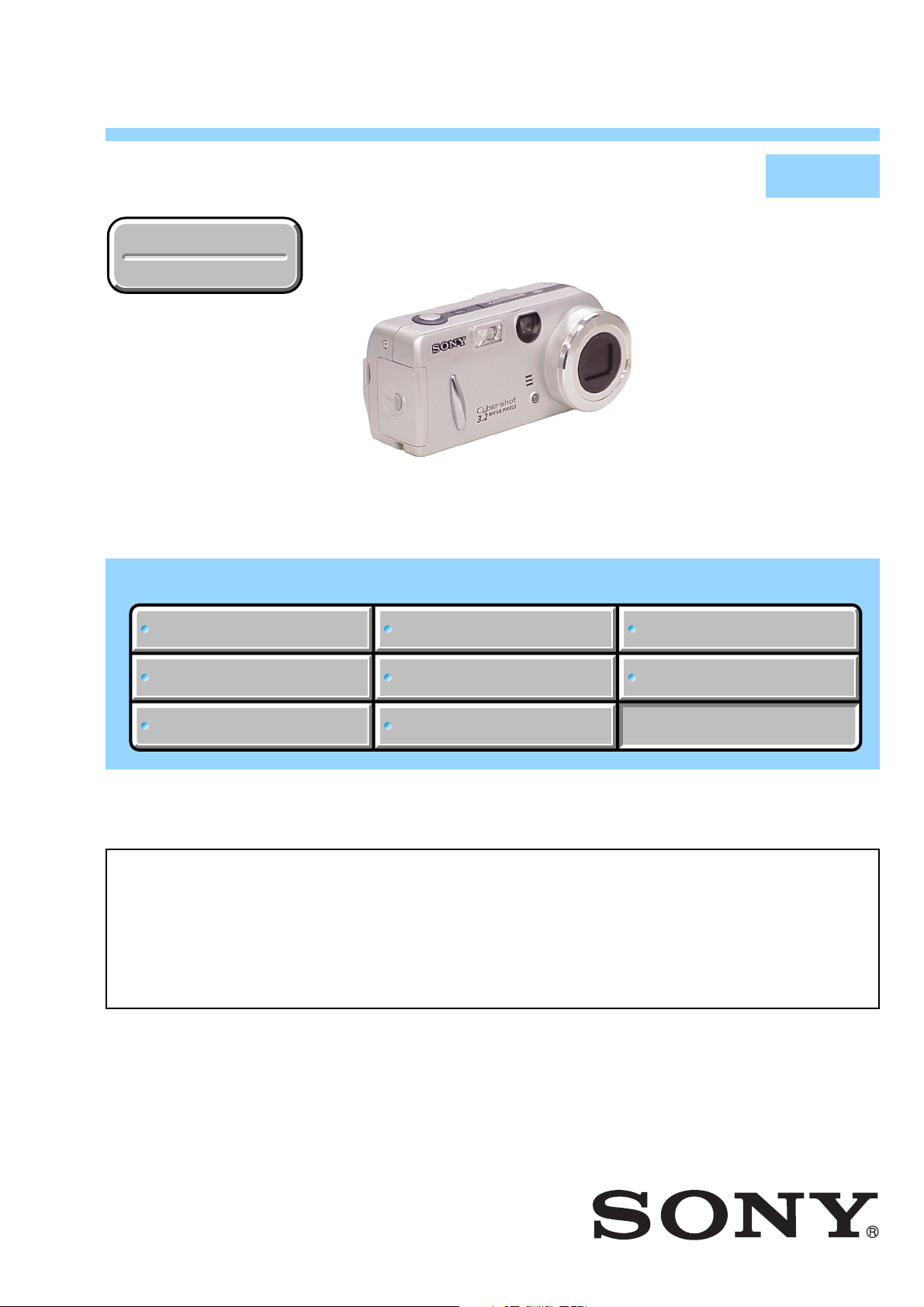
DSC-P52
SERVICE MANUAL
Ver 1.0 2003. 03
Revision History
Revision History
Link
Link
SPECIFICATIONS
BLOCK DIAGRAMS
BLOCK DIAGRAMS
LEVEL 2
US Model
Canadian Model
AEP Model
UK Model
E Model
Australian Model
Hong Kong Model
Korea Model
Chinese Model
Tourist Model
Brazilian Model
PRINTED WIRING BOARDS
PRINTED WIRING BOARDSSPECIFICATIONS
SERVICE NOTE
SERVICE NOTE
DISASSEMBLY
DISASSEMBLY
• For INSTRUCTION MANUAL, refer to SERVICE MANUAL, LEVEL 1 (987624841.pdf).
• Reference No. search on printed wiring boards is available.
On the SY-91 board
This service manual provides the information that is premised the circuit board replacement service and not intended repair
inside the SY-91 board.
Therefore, schematic diagram, printed wiring board, waveforms, mounted parts location and electrical parts list of the SY-91
board are not shown.
The following pages are not shown.
Schematic diagram .............................Pages 4-7 to 4-26
Printed wiring board ............................Pages 4-39 to 4-42
Waveforms ...........................................
FRAME SCHEMATIC DIAGRAMS
FRAME SCHEMATIC DIAGRAMS
SCHEMATIC DIAGRAMS
SCHEMATIC DIAGRAMS
Mounted parts location .............................
Electrical parts list ................................... Pages 5-7 to 5-13
Pages 4-45 to 4-46
REPAIR PARTS LIST
REPAIR PARTS LIST
Page 4-48
DIGITAL STILL CAMERA
Page 2
DSC-P52
COVER
COVER
x Camera
[System]
Image device 6.67 mm (1/2.7 type) color
Total pixels number of camera
Effective pixels number of camera
Lens
Exposure control
White balanceAutomatic, Daylight, Cloudy,
File format (DCF compliant)
Recording media
Flash Recommended distance
[Output connectors]
A/V OUT (MONO) jack (Monaural)
USB jack mini-B
CCD
Primary color filter
Approx. 3 340 000 pixels
Approx. 3 210 000 pixels
2× zoom lens
f=6.3 to 12.6 mm
(35 mm camera conversion: 41 to
82 mm (1
F3.8
Automatic, Program, Twilight,
Twilight portrait, Landscape, Snow,
Beach
Fluorescent, Incandescent
Still images: Exif Ver. 2.2, JPEG
compliant, GIF (for Clip Motion),
DPOF compatible
Audio with still image: MPEG1
compliant (Monaural)
Movies: MPEG1 compliant
(Monaural)
“Memory Stick”
0.5 to 3.3 m (19
10 feet 9
Minijack
Video: 1 Vp-p, 75 Ω, unbalan ced,
sync negative
Audio: 327 mV (at a 47 kΩ load)
Output impedance 2.2 kΩ
5
/8 to 3 1/4 inches))
3
/4 inches to
29
/32 inches)
SPECIFICATIONS
[LCD screen]
LCD panel used
Total number of dots
[Power, general]
Power AA nickel hydride batteries (2)
Power consumption (when recording)
Operating temperature range
Storage temperature range
Dimensions
Mass
Microphone Electret condenser microphone
Speaker Dynamic speaker
x BC-CS2A/CS2B Ni-MH battery
charger
Power requirements
Output voltage
Operating temperature range
Dimensions 71 × 30 × 91 mm
Mass Approx. 90 g (3 oz)
4.0 cm (1.6 type) TFT drive
61 600 (280×220) dots
2.4 V
AC-LS5 AC Adaptor
(not supplied), 4.2 V
1.6W
0° to +40°C (32° to +104°F)
–20° to +60°C (– 4 ° to +140°F)
123.2
× 57.7 × 52 mm
7
3
(4
/
× 2
/8 × 2 1/8 inches)
8
Approx. 280 g (9.9 oz) (two
batteries, “Memory Stick” and wrist
strap included)
AC 100 to 240V 50/60Hz
3 W
AA : DC 1.4 V 400 mA × 2
AAA : DC 1.4 V 160 mA × 2
0° to +40°C (32° to +104°F)
7
3
/
× 3
16
5
/8 inches) (W/H/
/
× 1
(2
8
D)
x AC-LS5 AC Adaptor (not supplied)
Power requirements
Rated output voltage
Operating temperature range
Storage temperature range
Dimensions 48 × 29 × 81 mm (1
Mass Approx. 180 g (6 oz)
AC 100 to 240 V, 50/60 Hz
11 W 0.16 to 0.09 A
DC 4.2 V, 1.5 A
0° to +40°C (32° to +104°F)
–20° to +60°C (–4° to +140°F)
1
3
/4 inches) (W/H/D, protruding
parts not included)
(adaptor only)
15
/16 × 1 3/16
Accessories
HR6 (size AA) Ni-MH batteries (2)
Battery case
BC-CS2A/CS2B Ni-MH Battery charger (1)
Power cord (mains lead) (1)
USB cable (1)
A/V connecting cable (1)
Wrist strap (1)
“Memory Stick” (16MB) (1)
CD-ROM (USB driver: SPVD-010) (1)
Operating Instructions (1)
Design and specifications are subject to change
without notice.
CAUTION :
Danger of explosion if battery is incorrectly replaced.
Replace only with the same or equivalent type.
SAFETY-RELATED COMPONENT WARNING!!
COMPONENTS IDENTIFIED BY MARK 0 OR DOTTED LINE WITH
MARK 0 ON THE SCHEMATIC DIAGRAMS AND IN THE PARTS
LIST ARE CRITICAL TO SAFE OPERATION. REPLACE THESE
COMPONENTS WITH SONY PARTS WHOSE PART NUMBERS
APPEAR AS SHOWN IN THIS MANUAL OR IN SUPPLEMENTS
PUBLISHED BY SONY.
ATTENTION AU COMPOSANT AYANT RAPPORT
À LA SÉCURITÉ!
LES COMPOSANTS IDENTIFÉS PAR UNE MARQUE 0 SUR LES
DIAGRAMMES SCHÉMATIQUES ET LA LISTE DES PIÈCES SONT
CRITIQUES POUR LA SÉCURITÉ DE FONCTIONNEMENT. NE
REMPLACER CES COMPOSANTS QUE PAR DES PIÈSES SONY
DONT LES NUMÉROS SONT DONNÉS DANS CE MANUEL OU
DANS LES SUPPÉMENTS PUBLIÉS PAR SONY.
— 2 —
Page 3

SAFETY CHECK-OUT
After correcting the original service problem, perform the following
safety checks before releasing the set to the customer.
DSC-P52
1. Check the area of your repair for unsoldered or poorly-soldered
connections. Check the entire board surface for solder splashes
and bridges.
2. Check the interboard wiring to ensure that no wires are
"pinched" or contact high-wattage resistors.
3. Look for unauthorized replacement parts, particularly
transistors, that were installed during a previous repair. Point
them out to the customer and recommend their replacement.
4. Look for parts which, through functioning, show ob vious signs
of deterioration. Point them out to the customer and
recommend their replacement.
5. Check the B+ voltage to see it is at the values specified.
6. Flexible Circuit Board Repairing
• Keep the temperature of the soldering iron around 270˚C
during repairing.
• Do not touch the soldering iron on the same conductor of the
circuit board (within 3 times).
• Be careful not to apply force on the conductor when soldering
or unsoldering.
Unleaded solder
Boards requiring use of unleaded solder are printed with the leadfree mark (LF) indicating the solder contains no lead.
(Caution: Some printed circuit boards may not come printed with
the lead free mark due to their particular size.)
: LEAD FREE MARK
Unleaded solder has the following characteristics.
• Unleaded solder melts at a temperature about 40°C higher than
ordinary solder.
Ordinary soldering irons can be used but the iron tip has to be
applied to the solder joint for a slightly longer time.
Soldering irons using a temperature regulator should be set to
about 350°C.
Caution: The printed pattern (copper foil) may peel away if the
heated tip is applied for too long, so be careful!
• Strong viscosity
Unleaded solder is more viscous (sticky, less prone to flow) than
ordinary solder so use caution not to let solder bridges occur such
as on IC pins, etc.
• Usable with ordinary solder
It is best to use only unleaded solder but unleaded solder may
also be added to ordinary solder.
— 3 —
Page 4

DSC-P52
TABLE OF CONTENTS
1. SERVICE NOTE ........................................................1-1
4-5. MOUNTED PARTS LOCATION ·································4-47
2. DISASSEMBLY
2-1. CABINET (REAR) BLOCK ASSEMBLY ·····················2-2
2-2. BLOCK LIGHT GUIDE PLATE, LCD MODULE,
CONTROL SWITCH BLOCK (SW-392), LITHIUM
BATTERY ·······································································2-3
2-3. MAIN BLOCK ASSEMBLY ··········································2-4
2-4. UNIT PARTS (UA-003), DC 8C-028G MOTOR ···········2-4
2-5. OPTICAL FINDER (B148B), VIDEO LENS (B147A),
CCD BLOCK ASSEMBLY ············································2-5
2-6. CONTROL SWITCH BLOCK (RL-060),
ST-82 BOARD ································································2-5
2-7. MEMORY STICK CONNECTOR,
JK-BLOCK (JK-256) ······················································2-6
2-8. SY-91 BOARD ································································2-7
2-9. OPTICAL FINDER (B148B), VIDEO LENS (B147A) ···2-9
2-10. FLASH UNIT ··································································2-9
2-11. CIRCUIT BOARDS LOCATION ·································2-10
2-12. FLEXIBLE BOARDS LOCATION ······························2-11
HELP (List of caution points is shown here)
3. BLOCK DIAGRAMS
3-1. OVERALL BLOCK DIAGRAM ····································3-1
3-2. CAMERA BLOCK DIAGRAM ·····································3-3
3-3. FRONT/LCD BLOCK DIAGRAM ································ 3-5
3-4. POWER BLOCK DIAGRAM·········································3-7
4. PRINTED WIRING BOARDS AND
SCHEMATIC DIAGRAMS
4-1. FRAME SCHEMATIC DIAGRAM (1/2) ·······················4-1
FRAME SCHEMATIC DIAGRAM (2/2) ·······················4-3
4-2. SCHEMATIC DIAGRAMS
Mounted parts location of the SY-91 board is not shown.
Page 4-48 is not shown.
5. REPAIR PARTS LIST
5-1. EXPLODED VIEWS ······················································ 5-1
5-1-1.CABINET (FRONT) SECTION ·····································5-3
5-1-2.CABINET (REAR) BLOCK SECTION ·························5-4
5-1-3.MAIN BLOCK SECTION-1···········································5-5
5-1-4.MAIN BLOCK SECTION-2···········································5-6
5-2. ELECTRICAL PARTS LIST ········································5-14
Parts list of the SY-91 board are not shown.
Pages from 5-7 to 5-13 are not shown.
Shematic diagram of the SY-91 board are not shown.
Pages from 4-7 to 4-26 are not shown.
• ST-82 (FLASH DRIVE)/FP-643 FLEXIBLE
SCHEMATIC DIAGRAM ····························4-27
• JK BLOCK (JK-256) (JACK)
SCHEMATIC DIAGRAM ····························4-29
• CONTROL SWITCH BLOCK (SW-392)
(LCD, CONTROL SW)
SCHEMATIC DIAGRAM ····························4-31
• RL-060 (POWER/SHUTTER SW)
SCHEMATIC DIAGRAM ····························4-33
• UA-003 (AF LED, SW)
SCHEMATIC DIAGRAM ····························4-34
4-3. PRINTED WIRING BOARDS
• ST-82 (FLASH DRIVE)
PRINTED WIRING BOARD ·······················4-37
Printed wiring board of the SY-91 board are not shown.
Pages from 4-39 to 4-42 are not shown.
• JK BLOCK (JK-256) (JACK)
FLEXIBLE BOARD·····································4-43
4-4. WAVEFORMS ······························································4-45
Waveforms of the SY-91 board are not shown.
Pages 4-45 to 4-46 are not shown.
— 4 —
Page 5
DSC-P52
COVER
COVER
SECTION 1
SERVICE NOTE
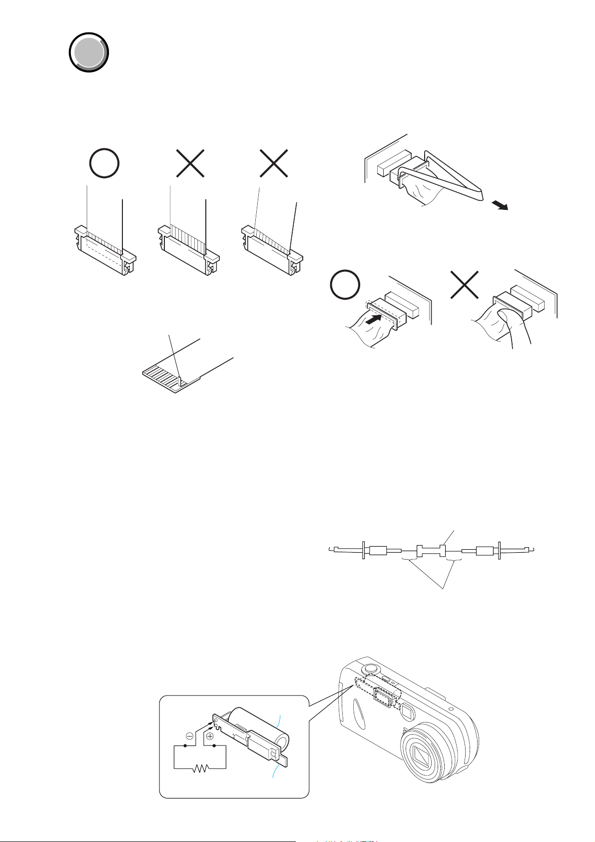
• NOTE FOR REPAIR
Make sure that the flat cable and flexible board are not cracked of
bent at the terminal.
Do not insert the cable insufficiently nor crookedly.
Cut and remove the part of gilt
which comes off at the point.
(Take care that there are
some pieces of gilt left inside)
When remove a connector, don't pull at wire of connector.
Be in danger of the snapping of a wire.
When installing a connector, don't press down at wire of connector.
Be in danger of the snapping of a wire.
[Discharging of the FLASH unit’s charging capacitor]
The charging capacitor of the FLASH unit is charged up to the
maximum 300 V potential.
There is a danger of electric shock by this high voltage when the
capacitor is handled by hand. The electric shock is caused by the
charged voltage which is kept without discharging when the main
power of the DSC-P52 is simply turned off. Therefore, the remaining
voltage must be discharged as described below.
Preparing the Short Jig
To preparing the short jig. a small clip is attached to each end of a
resistor of 1 kΩ /1 W (1-215-869-11)
Wrap insulating tape fully around the leads of the resistor to prevent
electrical shock.
Discharging the Capacitor
Short circuits between the positive and the negative terminals of
charged capacitor with the short jig about 10 seconds.
1 kΩ/1 W
Wrap insulating tape.
Shorting jig
(1k
Ω
/ 1w)
Capacitor
ST-82 board
1-1
Page 6
DSC-P52
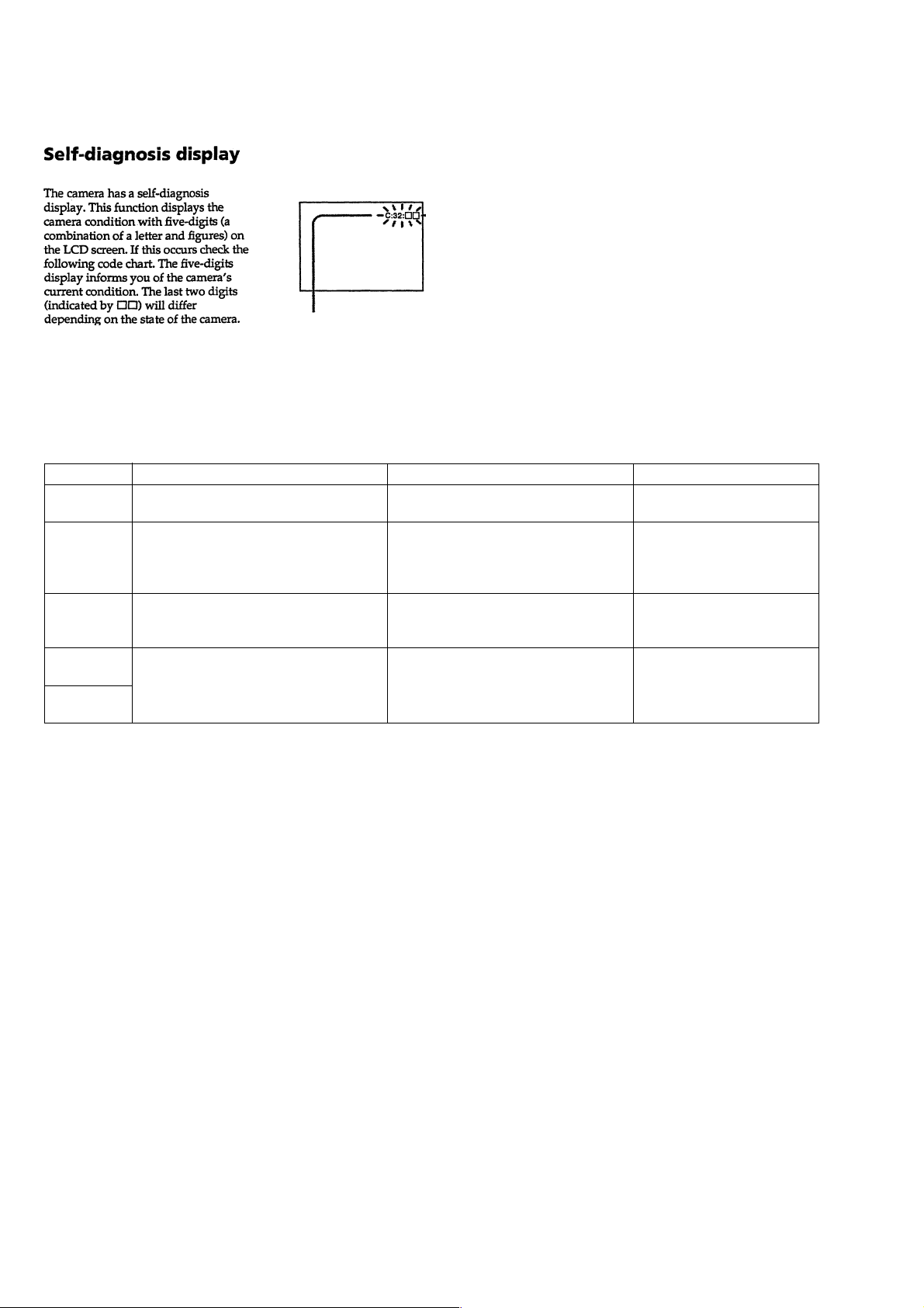
[Description on Self-diagnosis Display]
Self-diagnosis display
• C: ss: ss
• E: ss: ss
The contents which can be handled
by customer, are displayed.
The contents which can be handled
by engineer, are displayed.
Display Code
C:32:01
C:13:01
E:91:01
E:61:00 *1
E61:10 *1
Note : The error code is cleared if the battery is removed, except defective flash unit.
*1: The error display is given in two ways.
Turn off the main power then back on.
Replace the memory stick.
Format the memory stick with the DSC-P52.
Checking of flash unit or replacement of
flash unit.
Checking of lens drive circuit
Countermeasure
Trouble with hardware.
• The type of memory stick that cannot be
used by this machine, is inserted.
• Data is damaged.
• Unformatted memory stick is inserted.
Abnormality when flash is being
charged.
When failed in the focus initialization.
Cause
Caution Display During Error
SYSTEM ERROR
MS ERROR
Flash LED
Flash display
Flashing at 3.2 Hz
—
1-2E
Page 7
DSC-P52
COVER
COVER
SECTION 2
DISASSEMBLY
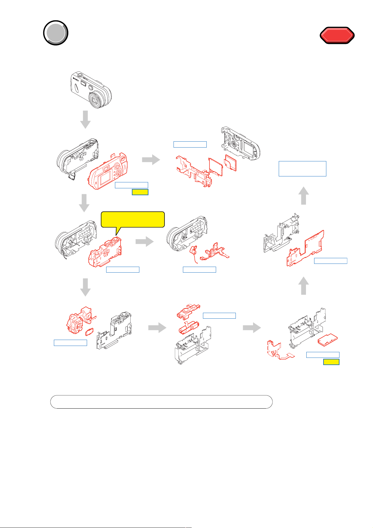
The following flow chart shows the disassembly procedure.
DISASSEMBLY
DISASSEMBLY
HELP
SY-91 board
service position
HELP
HELP
DISASSEMBLY
Discharging the Capacitor
DISASSEMBLY
DISASSEMBLY DISASSEMBLY
DISASSEMBLY
DISASSEMBLY
HELP
PROCEDURE OF REMOVING THE SY-91 BOARD (SERVICE POSITION)
1 2-1. CABINET (REAR) BLOCK ASSEMBLY .........................................................................
2 2-2. BLOCK LIGHT GUIDE PLATE, LCD MODULE, ............................................................
CONTROL SWITCH BLOCK (SW-392), LITHIUM BATTERY
3 2-3. MAIN BLOCK ASSEMBLY .............................................................................................
4 2-4. UNIT PARTS (UA-003), DC 8C-028G MOTOR .............................................................
5 2-5. OPTICAL FINDER (B148B), VIDEO LENS (B147A), CCD BLOCK ASSEMBLY ..........
6 2-6. CONTROL SWITCH BLOCK (RL-060), ST-82 BOARD ................................................
7 2-7. MEMORY STICK CONNECTOR, JK BLOCK (JK-256) ................................................
8 2-8. SY-91 BOARD ...............................................................................................................
2-1
(page 2-2)
(page 2-3)
(page 2-4)
(page 2-4)
(page 2-5)
(page 2-5)
(page 2-6)
(page 2-7)
Page 8
DSC-P52
NOTE: Follow the disassembly procedure in the numerical order given.
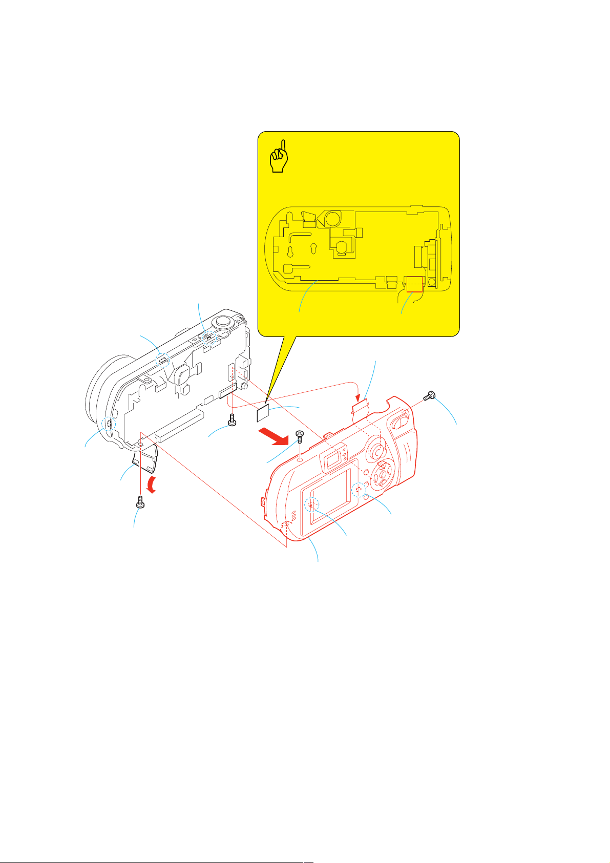
2-1. CABINET (REAR) BLOCK ASSEMBLY
Attach the Tape (Y) as shown in the illustration.
6
Claw
Caution
7
8
Claw
4
Open the MS lid.
Claw
5
Screw (M2 × 4),
lock ace, p2
3
Screw (M2 × 4),
lock ace, p2
2
Screw (M2 × 4),
lock ace, p2
SY-91 board
qa
Tape (Y)
Tape (Y)
qs
Control switch block (SW-392)
(39P)
q;
Claw
9
Claw
qd
Cabinet (rear) block assembly
1
Screw (M2 × 4),
lock ace, p2
2-2
Page 9
DSC-P52
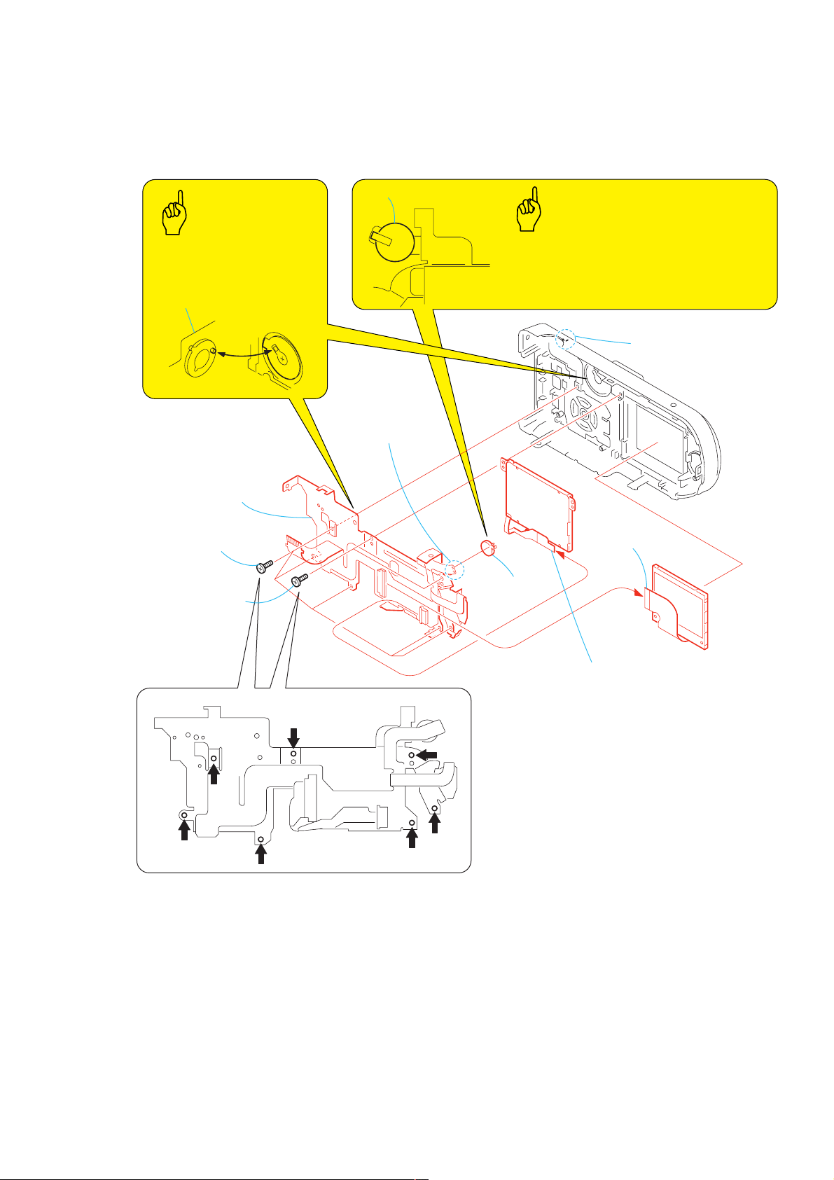
2-2. BLOCK LIGHT GUIDE PLATE, LCD MODULE, CONTROL SWITCH BLOCK (SW-392),
LITHIUM BATTERY
Lithium battery
Caution
When installing it,
align the switch position
as shown.
Control switch block (SW-392)
6
Control switch block (SW-392)
1
Five tapping screws
×
(M1.7
2
(M1.7
4)
Two tapping screws
×
4)
7
Remove soldering
from the two points.
Caution
Danger of explosion if battery is incorrectly replaced.
Replace only with the same or equivalent type.
3
Claw
5
LCD module (24P)
8
Lithium battery
4
Block light guide plate (6P)
2-3
Page 10
DSC-P52
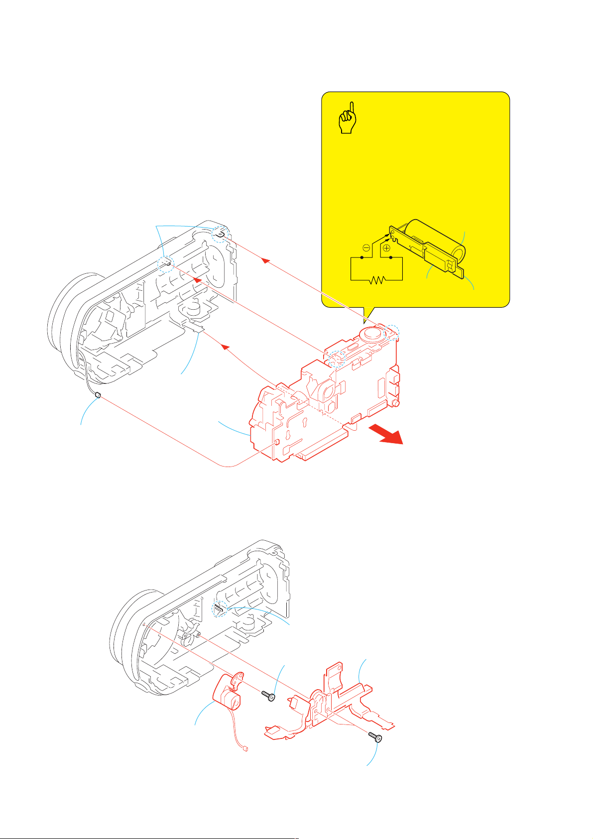
2-3. MAIN BLOCK ASSEMBLY
3
Two claws
Caution
The power supply capacitor of the Flash unit is
charged to the voltage as high as 300 V at a
maximum. The high voltage is not discharged
even after the main power of the machine is
simply turned off and the charged potential still
remains.
Discharge the residual voltage by referring to
Service Note (page 1-1).
Capacitor
1
Unit parts (UA-003)
(10P)
4
Main block assembly
2
DC 8C-028G motor (2P)
2-4. UNIT PARTS (UA-003), DC 8C-028G MOTOR
Shorting jig
Ω
/ 1w)
(1k
Flash unit
ST-82 board
5
DC 8C-028G motor
2
Claw
4
Tapping screw, p2
(1.7 × 5)
2-4
3
Unit parts (UA-003)
1
Two tapping screws, p2
×
(1.7
5)
Page 11
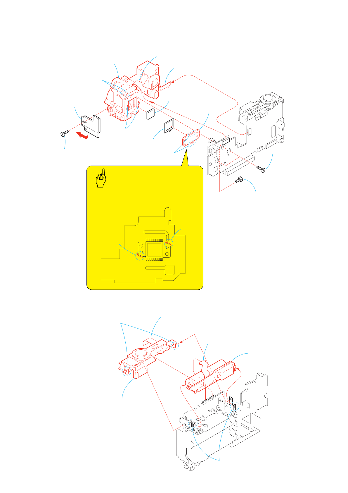
2-5. OPTICAL FINDER (B148B), VIDEO LENS (B147A), CCD BLOCK ASSEMBLY
q;
Optical filter block
9
Optical finder (B148B), video lens (B147A)
1
FP689 flexible board (21P)
2
Optical finder (8P)
qs
Remove the solderings.
qd
CCD block assembiy
5
Two tapping screws ,p2
(1.7 × 5)
3
Tapping screw
(1.7 × 4)
6
Tapping screw
(1.7 × 4)
4
Lens frame (R)
8
two bosses
7
T
wo bosses
qa
Seal rubber (DQ)
Caution
mark
mark
When installing the CCD block assy,
align the CCD block assy with the mark as shown
in the illustration.
d
DSC-P52
2-6. CONTROL SWITCH BLOCK (RL-060), ST-82 BOARD
1
Two claws
3
Control switch block (RL-060)
2
(10P)
Control switch block (RL-060)
5
FP-643 flexible board
(12P)
6
ST-82 boar
2-5
4
Two claws
Page 12
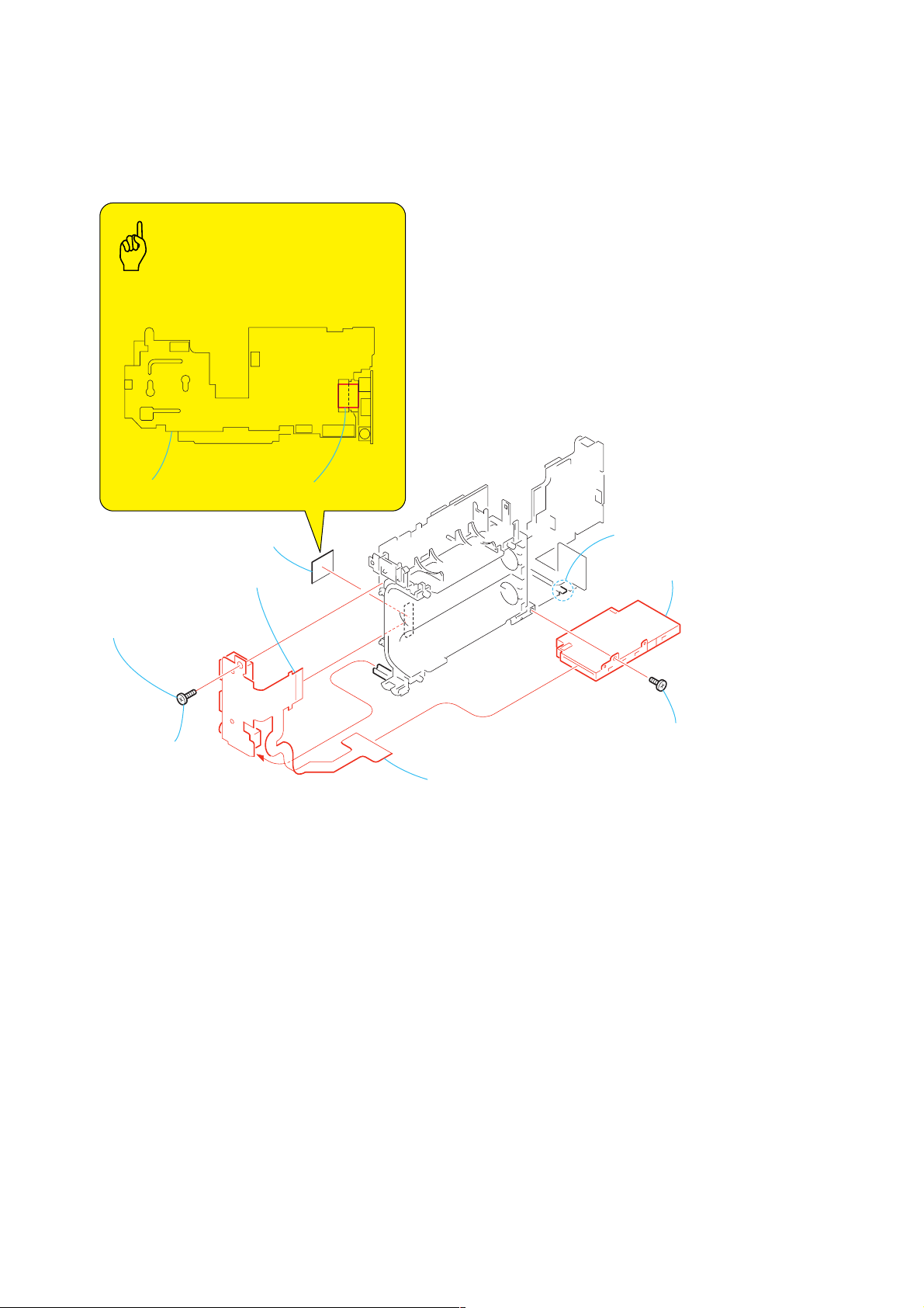
DSC-P52
r
2-7. MEMORY STICK CONNECTOR, JK BLOCK (JK-256)
Caution
Attach the Tape (Y) as shown in the illustration.
SY-91 board
7
(39P)
8
JK BLOCK (JK-256)
5
Tapping screw, p2
×
(1.7
5)
6
Tape (Y)
JK BLOCK (JK-256)
Tape (Y)
3
JK BLOCK (JK-256)
(10P)
2
Claw
4
Memory stick connecto
1
Tapping screw
×
(1.7
4)
2-6
Page 13
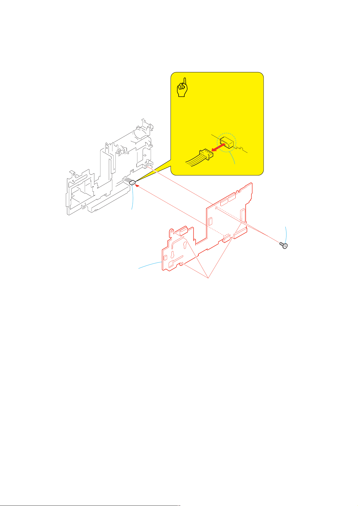
2-8. SY-91 BOARD
)
DSC-P52
Caution
When removing the harness,
be sure to pull the harness up at the
right angle with the board while pressing
down the connector on the circuit board.
Connector
2
Battery holder (with terminal)(4P)
3
SY-91 board
1
Four screws(M1.7 × 2.5
2-7
Page 14
DSC-P52
N
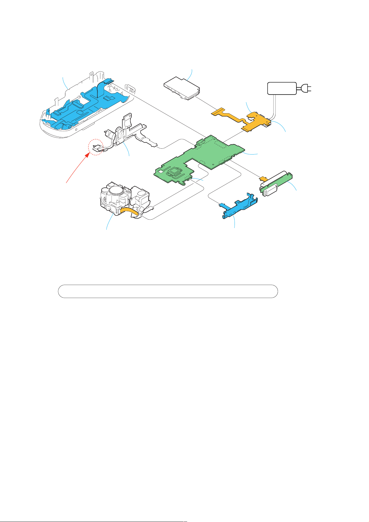
[SERVICE POSITION (SY-91 BOARD)]
Cabinet (rear) block assembly
(39P)
Memory stick connector
(10P)
JK BLOCK
(JK-256)
AC power
adaptor
AC I
By using an adhesive tape,
press the SENCV OPEN switch.
Optcal finder (B148B), video lens (B147A)
“ Never remove the lens unless removal
is required at the event of checking the
CCD imager and others.’’
PROCEDURE OF REMOVING THE SY-91 BOARD (SERVICE POSITION)
1 2-1. CABINET (REAR) BLOCK ASSEMBLY .........................................................................
2 2-2. BLOCK LIGHT GUIDE PLATE, LCD MODULE, ............................................................
CONTROL SWITCH BLOCK (SW-392), LITHIUM BATTERY
3 2-3. MAIN BLOCK ASSEMBLY .............................................................................................
4 2-4. UNIT PARTS (UA-003), DC 8C-028G MOTOR .............................................................
5 2-5. OPTICAL FINDER (B148B), VIDEO LENS (B147A), CCD BLOCK ASSEMBLY ..........
6 2-6. CONTROL SWITCH BLOCK (RL-060), ST-82 BOARD ................................................
7 2-7. MEMORY STICK CONNECTOR, JK BLOCK (JK-256) ................................................
8 2-8. SY-91 BOARD ...............................................................................................................
Unit parts (UA-003)
(21P)
(10P)
(8P)
CN706
CN702
CN701
CN203
CN201
Control switch block (RL-060)
CN704
CN705
(10P)
(39P)
SY-91 board
(12P)
(page 2-2)
DC jack
ST-82 board
(page 2-3)
(page 2-4)
(page 2-4)
(page 2-5)
(page 2-5)
(page 2-6)
(page 2-7)
2-8
Page 15

2-9. OPTICAL FINDER (B148B), VIDEO LENS (B147A)
)
1
Tapping screw
(1.7
×
4)
3
T
wo bosses
4
Optical finder (B148B)
2
Two tapping screws
(1.7
×
4)
5
FP689 flexible board (21P
6
Video lens (B147A)
DSC-P52
2-10.FLASH UNIT
2
Flash unit
1
Remove soldering
from the two points.
2-9
Page 16

DSC-P52
2-11.CIRCUIT BOARDS LOCATION
ST-82
SY-91
Board Name Function
SY-91
ST-82 FLASH DRIVE
CCD IMAGER CAMERA A/D CONV., LENS DRIVE, CAMERA DSP, VIDEO AMP, SH DSP,
CLK GEN, LCD DRIVE TIMING GENERATOR,FRONT CONTROL, AUDIO I/O, DC IN,
DC-DC CONVERTER, CONNECTOR
2-10
Page 17

K
2-12.FLEXIBLE BOARDS LOCATION
The flexible boards contained in the VIDEO LENS are not shown.
DSC-P52
CONTROL SWITCH BLOC
(SW-392)
CONTROL SWITCH BLOCK
(RL-060)
UNIT PARTS (UA-003)
FP-643
JK BLOCK
(JK-256)
FP-689
2-11E
Page 18

HELP
Sheet attachment positions and procedures of processing the flexible boards/harnesses are shown.
MAIN BLOCK SECTION
DSC-P52
19/Mar/2003. Update
SY-91 board SY-91 board
Caution A (260) label
Tape (Y)
SY-91 board
Busteraid 260
Caution B (260) label
SY-91 board
HELP
Page 19

COVER
COVER
Link
Link
DSC-P52
3. BLOCK DIAGRAMS
OVERALL BLOCK DIAGRAM
OVERALL BLOCK DIAGRAM
FRONT/LCD BLOCK DIAGRAM
FRONT/LCD BLOCK DIAGRAM
POWER BLOCK DIAGRAMCAMERA BLOCK DIAGRAM
POWER BLOCK DIAGRAMCAMERA BLOCK DIAGRAM
Page 20

DSC-P52
COVER
COVER
3-1. OVERALL BLOCK DIAGRAM
SY-91 BOARD
X781
27MHz
4
2
4
4
2
(1/10)
IC351
CCD
IMAGER
LENS BLOCK
IRIS
IRIS
M
METER
H
SHUTTER
MOTOR
M
FOCUS
MOTOR
M
ZOOM
MOTOR
M
ZOOM RESET
SENSOR
FOCUS RESET
SENSOR
LENS TEMP
SENSOR
OVF RESET
SENSOR
FP-689
(FLEXIBLE)
LENS BARIA CLOSE
LENS BARIA OPEN
SECTION 3
3. BLOCK DIAGRAMS
3. BLOCK DIAGRAMS
BLOCK DIAGRAMS
( ) : Number in parenthesis ( ) indicates the division number of schematic diagram where the component is located.
14
(3/10)
IC301
CAMERA
DSP
(HM (3M SA)
BOARD)
PANEL R,G,B
3
PANEL V,HD O
2
YO
A OUT L
A IN
ADDRESS BUS
(4/10)
IC502
EEPROM
SYS V
STRB ON
2
DATA BUS
CONTROL
SIG
(4/10)
IC501
MC CAM
SH DSP
V AMP ON
4
MS DIO,MS SCLK,MS BS
USB DATA+/-
FR SI,FR SO,XFR SCK
XCAM SO,XCAM SCK
(3/10)
IC601
VIDEO
AMP
(7/10)
IC151
AUDIO
AMP
(6/10)
IC401
FRONT
CONT
IC781
IC203
IC201
(2/10)
(4/10)
CLOCK
GEN.
CCD OUT
H1,H2
V1,V2,V3A,V3B
V4,V5A,V5B,V6
V SUB
(2/10)
TG CLK
MC CLK1
USB CLK
(1/10)
IC901
CAMERA
MODULE
(CH-122
(3M)
BOARD)
(2/10)
DRIVER
IC202
7ch LENS
DRIVER
SHUTTER
DRIVER
FOCUS
MOTOR
DRIVER
MOTOR
DRIVER
(2/10)
IC205
SHUTTER
DRIVER
(2/10)
IC204
D/A CONV
DATA BUS
CLK TG
CCD FD,CLD HD
XCAM SO,XCAM SCK
IRIS
ZOOM
2
XCAM SO,XCAM SCK
SP VOL
(5/10)
IC801
LCD
DRIVER
(5/10)
IC802
LCD
TG
CONTROL
(SW-392)
(FLEXIBLE)
2
JK-256(2/2)
(FLEXIBLE)
(FLEXIBLE)
(SHUTTER)
VR,VG,VB
SWITCH
BLOCK
(1/2)
BL H
UA-003
S101,102
SENCV
OPEN/CLOSE
V OUT
AV JACK IN
AU OUT
XMS IN
USB JACK IN
RL-060
S002
POWER
S003
PANEL UNIT
LCD901
COLOR
LCD
MONITOR
ND901
BACK LIGHT
SP901
SPEAKER
MIC901
MIC
J102
A/V OUT
(MONO)
CN101
(MS SOCKET)
(USB)
J101
DC IN
BT901
BATTERY
TERMINAL
JK-256 (1/2)
(FLEXIBLE)
ACV UNREG
BATT/ XEXT
BATT UNREG
EVER 4V
ACV UNREG
ST UNREG
(9/10)
IC001
DC/DC
CONVERTER
UNREG SO,UNREG SCK
SYS DD ON
D1.5V
D2.9V
A2.9V
PANEL 2.9V
PANEL 13.2V
PANEL -15.3V
D3.1V
A4.9V
PANEL 4.9V
M5V
CAM 15V
CAM-7.5
EVER 3V
BL H
(6/10)
IC402
INITIAL RESET
BACKUP VCC
KEY AD0,AD1
2
KEY AD3
MODEL DIAL
ST UNREG
FUNCTION
KEY
ZOOM
SWITCH
4 MODE
DIAL
S109
RESET
BT100
LITHIUME
BATTERY
(SECONDARY)
ST UNREG
STB CHARGE
XSTB FULL
STB ON
CONTROL
SWITCH
(SW-392)
FP-643
(FLEXIBLE)
3-1 3-2
BLOCK
(2/2)
ST-82 BOARD
AUDIO SIGNAL
VIDEO SIGNAL
VIDEO/AUDIO SIGNAL
CHARGING
CAPACITOR
FLASH
UNIT
Page 21

DSC-P52
COVER
COVER
3. BLOCK DIAGRAMS
3. BLOCK DIAGRAMS
3-2. CAMERA BLOCK DIAGRAM
SY-91 BOARD (1/2)
(1/10) (1/10)
IC351
CCD
IMAGER
V OUT
V1
V2
V3A
V3B
X781
27MHz
CN203(1/2)
OVF A
8
OVF A
6
OVF B
5
OVF B
7
CN201
IRIS BIAS+
4
IRIS HALL+
6
IRIS HALL-
3
IRIS BIAS-
5
DRIVE+
2
DRIVE-
1
FOCUS A
FOCUS A
FOCUS B
FOCUS B
FOCUS A
FOCUS A
FOCUS B
FOCUS B
X ZM RST SENS
7
XFC RST SENS
8
LENS TEMP
CN203(2/2)
OVF RST SENS
1
CN202
2
1
V5A
V5B
CSUB
V4
V6
H1
H2
RG
2
LENS BLOCK
IRIS
IRIS
METER
M
H
SHUTTER
MOTOR
M
FOCUS
MOTOR
M
ZOOM
MOTOR
M
ZOOM RESET
SENSOR
FOCUS RESET
SENSOR
LENS TEMP
SENSOR
OVF
SENSOR
DC MOTOR
8C-028G
FP-689
(FLEXIBLE)
OVF A
OVF A
OVF B
OVF B
IRIS BIAS+
IRIS HALL+
IRIS HALL-
IRIS BIAS-
DRIVE+
DRIVE-
FOCUS A
FOCUS A
FOCUS B
FOCUS B
FOCUS A
FOCUS A
FOCUS B
FOCUS B
XZM RST SENS
XFC RST SENS
LENS TEMP
VFC RST SENS
M
LENS BARIA CLOSE
LENS BARIA OPEN
16
20
14
18
17
21
14
18
13
( ) : Number in parenthesis ( ) indicates the division number of schematic diagram where the component is located.
(3/10)
IC301
CAMERA DSP
(HM (3M SA) BOARD)
26
21
.
.
27
19
.
.
25
14
.
.
ADIN00
24
18
.
.
ADIN13
22
16
.
.
23
13
.
.
20
12
CLK TG
96
TG WEN
183
CCD HD
8
CCD FD
9
OPB CLP
6
DUM CLP
7
SUB CNTL
250
CLK
88
DIR 2A
242
DIR 2B
243
EN2
241
SHUTTER
246
M SHUT EN
196
DIR 0A
234
DIR 0B
235
EN0
233
DIR 1A
238
DIR 1B
239
EN1
237
SENS1
236
SENS0
232
SENS2
240
SENS2
187
D00
D15
A01
A25
AUCK
PLL BYP
WRLX
WRHX
RDX
CS XRAM
CSX
LCD VD
LCD HD
RSTX
NDVDO
STROB E1
SENCV OPEN
SENCV CLOSE
AOUT L
67
68
.
.
72
65
.
.
66
81
.
.
78
77
.
.
1616 DATA BUS
73
75
.
.
71
69
.
.
79
80
.
.
74
76
54
.
38
.
52
.
37
.
51
.
41
.
49
.
39
.
47
.
35
.
53
.
33
.
45
25
.
36
.
44
.
34
.
50
.
31
.
48
.
29
.
40
.
32
.
46
.
30
43
259
104
64XWAIT
62IRQIMG
59
60
55
58
57
RO
212
GO
207
BO
204
229
225
94
227
248
SENCV OPEN
201
SENCV CLOSE
190
YO
215
278
AIN
272
ADDRESS BUS
PANEL R
PANEL G
PANEL B
PANEL V
HDO
XRST SYS
SYS V
XRST SYS
STRB ON
10
8
7
6
5
4
3
2
1
17
18
12
14SUB
15
(4/10)
IC781
CLOCK GEN.
CLK3 OUT
FIN
CLK2 OUT
IC203(1/4)
BIAS CONT
Q201
CLK3 ON
CLK2 ON
REF OUT
(2/10)
HALL
7
6
Q352
Q204
IC205
BARRIER
DRIVER
4
11
5
13
16
7
IC203(2/4)
GAIN CONT
IC201(1/2)
IRIS DRIVE
MOTOR
TG CLK
USB CLK
TG CLK EN
USB CLK EN
MC CLK1
5
6
(2/10)
HALL
13
2
1
3
(2/10)
2
3
Q351
14
15
17
18
43
46
20
21
23
24
37
38
41
42
12
13
(2/10)
IC203(3/4)
AMP
7
(2/10)
IC201(2/2)
IRIS DRIVE
8
(2/10)(2/10)
IC203(4/4)
IRIS CONT
OUT1A
OUT1B
OUT2A
OUT2B
7ch LENS DRIVER
OUT7A
OUT7B
OUT3A
OUT3B
OUT4A
OUT4B
OUT5A
OUT5B
OUT6A
OUT6B
14
6
5
9
10
IRIS
DRIVER
(2/10)
IC202
SHUTTER
DRIVER
FOCUS
MOTOR
DRIVER
ZOOM
MOTOR
DRIVER
HALL OFFSET
HALL GAIN
HALL REF
IRIS CONT2
IRIS CONT1
IC901
CAMERA
MODULE
(CH-122 (3M) BOARD)
CCD OUT
6
V1
18
V2
10
V3A
19
V3B
20
V4
14
V5A
15
V5B
16
V6
17
H1
2
H2
3
RG
5
24
VHST
TG CLK
48
XCAM RST
IN1
12
IN2
10
EN1
11
EN2
9
48IN7
47EN7
IN3
8
IN4
6
EN3
7
EN4
5
IN5
4
IN6
2
EN5
3
EN6
1
PS
33
(2/10)
IC204
D/A CONV
A07
6 14
A06
5
A05
4
A02
1
A01
15
MCK12
CAHR
CAVR
CLPOB
CLPDM
XFE CS
XTG CS
DI
CLK
LD
A10
A03
WEN
25
D0
38
D13
49
55
46
47
43
44
41XCAM SO
42XCAM SCK
39
40
45
13
12
10
PRE LAMP AF ON
2
XCAM RESET
CAM SO
XCAM SCK
DAC STB
XCAM SO
XCAM SCK
XFE CS
XTG CS
SP VOL
14
1
(PAGE 3-5)
2
(PAGE 3-5)
3
(PAGE 3-5)
TH351
TEMP
SENSOR
XCAM SO
XCAM SCK
DAC STB
16
LCD
BLOCK
FRONT
BLOCK
FRONT
BLOCK
XFE CS
XTG CS
XCAM RESET
USB CLK
TG CLK EN
USB CLK EN
49
60
.
56
47
.
.
54
45
.
52
41
.
.
51
39
62
79
.
64
.
81
.
66
.
83
68
88
.
70
.
90
.
72
.
92
.
73
.
93
.
75
.
95
.
76
.
97
78
146
162
138
165
100
101
99
114
117
140
164
230
187
226
110
220
184
22
23
192
229
228
200
199
19
168
236
(4/10) (4/10)
IC501
MC CAM SH DSP
RXD2
203
TXD2
202
SCK2
204
CS
D0
D15
A1
A25
XCS PANEL TG
TCLK
SCL
WAIT
IRQ1
WE0
WE1
RD
CS4
CS6
USB D + PULLUP
RESETP
IRQ0
CCD TEMP
XAU LINE MUTE
CKIO
XFE CS
XTG CS
XCAM RESET
USB CLK
TG CLK EN
USB CLK EN
XCAM DR PS
LENS TEMP
HALL AD
TXD1
SCK1
DAC STB
LENS CLOSE ON
LENS OPEN ON
189
BUSY
14
71WE
190TXD0
RXD0
191
SCK0
185
SCS0
134
NMI
136
74UPDATA
157HELP
137
VG
232
V COM
235
35AE LOCK
MS DIR
216
215MS DIO
213MS SCLK
214MS BS
28
DP
239
DM
238
13
VAMP ON
29
50
XAU SP MUTE
CASU
124
25XAU PWR SAVE STBY
XCS PANEL TG
Q701(1/2)
LED
DRIVE
D3.1V
IC502
EEPROM
DO
4
DI
3
SCK
2
CS
1
BUSY
7
RST
6
FR SI
FR SO
XFR SCK
XCS MC
XMC NMI
MC UPDATA
MC HELP
V COM AD
Q501
FRONT
BLOCK
4
(PAGE 3-5)
VG
D2.9V
BLOCK
5
(PAGE 3-5)
D703
(AE/AF LOCK)
D705
(MS ACCESS)
7
6
C8
B2
G8
H9
H4
H5
J3
E1
F2
Q704
LED
DRIVE
LCD
FRONT
BLOCK
(PAGE 3-5)
VIDEO AMP
POWER SAVE
VIDEO IN
AUDIO AMP
LINE MUTE
SP SAVE
LPF SEL
PB IN
REC OUT
VOL CTL
BEEP
XBEEP MUTE
SELF TIMER LED
(3/10)
IC601
(7/10)
IC151
LINE OUT
MUTE DRVR
BEEP ON
XCAM SO
XCAM SCK
6
VOUT
SP OUT+
SP OUT-
MIC IN
MIC SPY
BEEP
4
B4
A5
A2
D1
B8
B9
XMS IN
USB JACK IN
AV JACK IN
FRONT
7
BLOCK
(PAGE 3-5)
8
BLOCK
(PAGE 3-5)
JK-256
(FLEXIBLE)
CN701
MS DIO
6
MS SCLK
4
MS BS
9
XMS IN
5
CN101
USB JACK IN
19
USB DATA+
22
USB DATA-
21
V OUT
17
AV JACK IN
15
AU OUT
13
VCC
1
3
2
(MS SOCKET)
D+
D-
J102
A/V OUT
(MONO)
(USB)
CONTROL SWITCH
BLOCK (SW-392)
3
2
5
AF ILLUMINATOR
9
.
10
3
1
(1/3)
SP+
SP-
MIC IN
D001
SELF TIMER
UA-003
(FLEXIBLE)
S102
SENCV OPEN
S101
SENCV CLOSE
AUDIO SIGNAL
VIDEO SIGNAL
VIDEO/AUDIO SIGNAL
A4.9V
SP901
SPEAKER
MIC901
MIC
CN702
(1/3)
CN706
LCD
3-3 3-4
Page 22

COVER
COVER
3. BLOCK DIAGRAMS
3. BLOCK DIAGRAMS
DSC-P52
3-3. FRONT/LCD BLOCK DIAGRAM
SY-91 BOARD (2/2)
(6/10)
IC401
FRONT
CONTROL
2
4
6
7
SYS V
XRST SYS
FR SI
FR SO
XFR SCK
XCS MC
XMC NMI
MC UPDATA
MC HELP
XMS IN
USB JACK IN
AV JACK IN
SELF TIMER LED
BEEP ON
BEEP
Q401
Q402(1/2)
Q403
MODU-
LATOR
X401
10MHz
X402
32.768kHz
SYS V
32
XRST SYS
77
FR SI
23
FR SO
24
XFR SCK
25
XCS MC
26
MC WAKEUP
80
XCS LCD
44
XMC HELP
36
MS IN
6
XUSB JACK IN
9
AV JACK IN
11
SELF TIMER LED
19
BEEP ON
49
MELODY
79
MELODY EN V
74
X1 IN
28
X1 OUT
29
X2 IN
52
X2 OUT
51
XAE LOCK ON
CAMERA
BLOCK
(PAGE 3-4)
CAMERA
BLOCK
(PAGE 3-4)
CAMERA
BLOCK
(PAGE 3-4)
CAMERA
BLOCK
(PAGE 3-4)
( ) : Number in parenthesis ( ) indicates the division number of schematic diagram where the component is located.
PWR LED ON
XPWR ON
XSHTR ON
CHARGE/STB
KEY AD0
PANEL R
PANEL G
1
8
XCS PANEL TG
VG
V COM AD
BL ON
BL LEVEL
BL H
BL THL
PANEL B
PANEL V
HDO
RST SYS
XCAM SO
XCAM SCK
CAMERA
BLOCK
(PAGE 3-4)
RL-060
(FLEXIBLE)
D002
Q402(2/2)
17
1
4
5
D2.9V
15XTALLY LED
Q701(2/2)
LED
16
DRIVE
55
56KEY AD1
58KEY AD3
54MODE DIAL
73XRESET
(6/10)
IC402
INITIAL RESET
BACKUP VCC
5RESET
3VBAT
7VIN
LED
DRIVE
D702
(SELF-TIMER/
RECORDING)
D704
(FLASH CHARGE)
EVER 4V
CN705
CN702
(2/3)
(POWER)
10
S002
POWER
5
3
1
S003
(SHUTTER)
CONTROL SWITCH
BLOCK (SW-392)
S100,104
S107,110
FUNCTION
34
S101,103
S105,108
FUNCTION
33
36
S102 S106
ZOOM
W
(INDEX)
MODE SW
35
38
5
4 MODE
BT100
LITHIUME
BATTERY
(SECONDARY)
(2/3)
KEY
KEY
DIAL
S109
RESET
D2.9V
T
CAMERA
(PAGE 3-4)
CAMERA
BLOCK
(PAGE 3-4)
POWER
BLOCK
(PAGE 3-7)
BLOCK
5
9
R IN
48
G IN
47
B IN
46
SI
40
XSCK
39
XCS
41
SO
45
SI
46
XSCK
42
XVD
48
HDI
1
XCLR
36
XCS
44
PWM
9
OP IN+8OP IN-
9
7
FILTER
29
BIAS
PD
10
OP OUT
27
OSC
11
OSCI
(5/10)
IC801
LCD
DRIVER
COM OUT
EXT DA2
EXT DA1
CN702
VR
20
VG
22
VB
24
27
37
35
(3/3)
22
23
24
16
VR
VG
VB
V COM
CN102
19
20
21
11
PANEL UNIT
LCD901
COLOR
LCD
MONITOR
CONTROL
SWITCH
11
12
13
14
15
17
18
19
20
21
30
29
BLOCK
(SW-392)
(3/3)
GRES
GPCK
GSRT
STBYB
RESET
SRT
OE
CLR
MCKJ
HCNT
BL H
BL THL
CN101
6
7
8
9
.
13
10
14
15
16
17
18
ND901
BACK LIGHT
4
3
VCO
D803
C818
L805
26
OSCO
(5/10)
IC802
LCD TG
BGP
33
37
XCLP39SBLK
BLACK IN
30
32
40
FRP
FRP
PFRP
29
41
COM FRP
28
XC SAVE38XP SAVE
45
25
XSTB
XC SABE
GSRT
SBTYB
RESET
SRT
CLR
MCKJ
HCNT
14GRES
15GPCK
16
17
18
20
OE
21
22
23
24
VIDEO SIGNAL
XSTB SAVE
STB CHG
XSTB FULL
CN501
Q501,502
10
12
3
9
4
1
Q503
Q504
TRANS
DRIVE
IC501
IGBT
DRIVER
42
T501
Q505
FLASH
CHARGE DET
D502
Q506
L501
ST-82
XE H
TRIGGER
XE L
FLASH
UNIT
BOARD
75
46
34
CAMERA
BLOCK
(PAGE 3-4)
CN704
ST UNREG
10
12
ST UNREG
FP-643
(FLEXIBLE)
XSTB PWR SAVE
3
STB CHARGE
9
4
STB ON
3
1
XSTB FULL
STB ON
3-5 3-6
Page 23

DSC-P52
COVER
COVER
3. BLOCK DIAGRAMS
3. BLOCK DIAGRAMS
3-4. POWER BLOCK DIAGRAM
SY-91 BOARD
CN001
1
BATT UINREG
J101
DC IN
BT901
BATTERY
TERMINAL
JK-256 (1/2)
(FLEXIBLE)
ACV UNREG
ACV GND
BATT/ XEXT
.
2
3
.
4
CN701
Q001
24
29
31
37
30
D002
D003
BATT /XETX
G1
4
G2
5
Q002
Q004,009
SWITCH
Q005
Q006
Q007
D1
S1
S1
D2
S2
S2
1
2
3
8
7
6
CHARGE
SWITCH
( ) : Number in parenthesis ( ) indicates the division number of schematic diagram where the component is located.
FAST CHARGE
UNREG SO
UNREG SCK
XCS DD CON
SYS DD ON
EVER 3.0V
F007
F001
F003
F005
BATT UNREG
ST UNREG
ACV UNREG
DC/DC CONVERTER
DATA
45
CLK
46
XCS
44
CONT
57
VCC1
56
RST
47
(9/10)
IC001
OUT1-P
OUT1-N
V-IN1
VCC3
OUT3-P
OUT3-N
V-IN3
VCC4
OUT4-P
OUT4-N
V-IN4
VCC5
OUT5-P
OUT5-N
OUT5-S
V-IN5
OUT6-P
OUT6-N
OUT6-S
V-IN6
OUT9-N
-IN (S) 9
OUT10
AMP IN
-IN10
AMP OUT
VCC2
OUT2-N
OUT2-P
OVP2
V-IN2
V+IN2
ON/OFF2
Q021,022
SWITCHING
L012
(8/10)
IC003
BATT
12
DET
D009
36
37
55
42
32
33
54
19
30
31
53
20
38
39
43
52
28
29
18
50
23
-IN9
80
1
22
4
3
5
41
35
34
58
60
61
48
L005
L003
L002
L001
Q012,018
SWITCHING
Q013,019
SWITCHING
Q016
SWITCHING
Q020,024
SWITCHING
Q017,023
SWITCHING
Q015
SWITCHING
Q011
SWITCHING
Q010
Q003
BACK LIGHT
SWITCHING
D004
D014
D016
D013
L006
L007
L008
D020
L009
L010
Q025
Q026
BL THH
BL H
BL THL
BL LEVEL
BL ON
BL L
CH1
CH3
CH4
CH5
CH6
Q014,027
SWITCHING
CH9
CH10
CH2
9
(8/10)
IC004
DC/DC
CONV
D12
LCD
DRIVER
(PAGE 3-5)
15
2
Q028-030
SWITCHING
M5V
D001
L011
DD CON SENS
PANEL -15.3V
PANEL 13.2V
CAM -7.5V
BATT UNREG
ST UNREG
ACV UNREG
EVER 4.0V
D1.5V
D2.9V
A2.9V
PANEL 2.9V
D3.1V
A4.9V
PANEL 4.9V
CAM 15V
BATT /XETX
FAST CHARGE
UNREG SO
UNREG SCK
XCS DD CON
SYS DD ON
L302
L502
L601
L163
L152
(6/10)
IC401
FRONT
CONT
(4/10) (2/10) (2/10)
IC781
FB781
CLOCK
GEN.
L206
L203
(2/10)
IC204
D/A
CONV.
(2/10)
IC205
SHUTTER
DRIVE
(3/10)
IC301
CAMERA
DSP
(HM (3M SA)
BOARD)
(4/10)
IC501
MC CAM
SH DSP
(4/10)
IC502
EEPROM
IC601
VIDEO
AMP
Q802
L205
L202
FB301
FB302
FB303
AU 2.9V
FB501
FB503
FB502
L501
(7/10) (3/10)
IC151
AUDIO
AMP
Q801
L401
STB CHARGE
IC201
IRIS
DRIVE
HALL REF
XLENS RST LED
CAM DD ON
MS POWER ON
L803
L804
L801
L802
XRESET
BATT IN
BACKUP VCC
EVER 3.0V
(2/10)
IC202
LENS
DRIVE
Q906
(1/2)
IC203
IRIS/HALL
CONT
L901
L902
L903
Q905
(1/2)
Q905
(2/2)
Q906
(2/2)
(5/10)
IC801
LCD
DRIVER
(5/10)
IC802
LCD
TG
(6/10)
IC402
INTIAL RESET
BACKUP VCC
Q205
FB902
FB904
FB903
FB905
FB906
Q703
CCD 15V
CCD -7.5V
Q702
Q702
(1/10)
IC901
CAMERA
MODULE
(CH-122
(3M)
BOARD)
D701
L351
FB351
STB CHARGE
FC SENS VCC
ZM SENS VCC
OVF SENS VCC
AF LED 4.9V
(1/10)
IC351
CCD
IMAGER
CN704
CN706
CN701
CN201
CN203
CN702
LI3V
10
12
9
2
2
7
.
8
2
.
3
8
9
2
7
9
26
10
31286
5
FP-643
(FLEXIBLE)
ST UNREG
STB CHARGE
M5V
UA-003
(FLEXIBLE)
D001
(SELF-TIMER/
AF ILLUMINATOR)
MS
PORT
JK-256(2/2)
(FLEXIBLE)
FP-689
(FLEXIBLE)
CN102
VGH
1
VGL
3
VSH
24
VDD
23
CONTROL
SWITCH
BLOCK
(SW-392)
CN101
BL L
BL THH
1
LITHIUME
BATTERY
(SECONDARY)
BT100
ST-82 BOARD
CN501
Q501,502
10
12
9
2
LENS ASSY
FOCUS
SENSOR
ZOOM
SENSOR
OVF
SENSOR
T501
IC501
IGBT
DRIVER
PANEL UNIT
LCD901
COLOR
LCD
MONITOR
ND901
BACK LIGHT
FLASH
UNIT
3-7 3-8E
Page 24

COVER
COVER
SECTION 4
PRINTED WIRING BOARDS AND SCHEMATIC DIAGRAMS
4-1. FRAME SCHEMATIC DIAGRAM (1/2)
1
2
DSC-P52
4-2. SCHEMATIC DIAGRAMS 4-3. PRINTED WIRING BOARDS
4-2. SCHEMATIC DIAGRAMS 4-3. PRINTED WIRING BOARDS
5
610 1612
8 15
9
1437114 1713
A
FLASH UNIT
ST-82 BOARD
OVF_NZM
S003
(SHUTTER)
B
CONTROL SWITCH BLOCK
(RL-060)
C
8
9EVER_3.0V
10PWR_LED
N.C.
D
8PCN203
1 OVF_SENS_RST
2 OVF_SENS_VCC
3 OVF_SENS_GND
4 N.C.
5 OVF_B
OVF_A
E
F
LENS BLOCK
G
FP-689
FLEXIBLE
H
6
OVF_B
7
8 OVF_A
CN201
1 DRIVE-
2 DRIVE+
3 HALL-
4 BIAS+
5 BIAS-
6 HALL+
7 XZM_RST_SENS
8 XFC_RST_SENS
9 ZM_SENS_VCC
10 FC_SENS_VCC
11 REG_GND
12 REG_GND
13 TEMP_OUT
14 FOCUS_B
15 ZOOM_B
16 FOCUS_A
17 ZOOM_A
FOCUS_B
18
19
ZOOOM_B
FOCUS_A
20
21
ZOOM_A
21P
10P
CN705
S002
POWER
1XAE_LOCK_SW
2N.C.
3XSHTR_ON
4
5XPWR_ON
6N.C.
7
N.C.
REG_GND
SY-91 BOARD(1/2)
12P
CN501
12P
CN704
1 STRB_ON
1STRB_ON
2 M_5V
2M_5V
3 XSTB_PWRSAVE
3XSTB_PWRSAVE
4 XSTB_FULL
5 REG_GND
6 REG_GND
FP-643
FLEXIBLE
4XSTB_FULL
5REG_GND
6REG_GND
7 REG_GND
8 REG_GND
7REG_GND
8REG_GND
9 STB_CHARGE
10 ST_UNREG
9STB_CHARGE
10ST_UNREG
11 ST_UNREG
12 ST_UNREG
11ST_UNREG
12
ST_UNREG
CN706
10P
MIC_GND
PRELAMP_AF_ON
1SENCV_OPEN
2REG_GND
3SENCV_CLOSE
4
5MIC_IN
6MIC_GND
7
8PRELAMP_AF_ON
9AF_LED_4.9V
10AF_LED_4.9V
AF
UA-003 UNIT
CN202
I
J
BT901
BATTERY TERMINAL
(DRY BATTERY)
2P
2 LENS_BARIA_CLOSE
1 LENS_BARIA_OPEN
CN001
4P
1 BATT_UNREG
2 BATT_UNREG
3 BATT_GND
4 BATT_GND
16
4-1 4-2
FRAME SCHEMATIC DIAGRAM (1/2)
Page 25

DSC-P52
COVER
COVER
FRAME SCHEMATIC DIAGRAM (2/2)
4-2. SCHEMATIC DIAGRAMS 4-3. PRINTED WIRING BOARDS
4-2. SCHEMATIC DIAGRAMS 4-3. PRINTED WIRING BOARDS
1
38
ND901
BACK-LIGHT
5 136
924 7
10
11 1514
12
A
LCD901
COLOR LCD
MONITOR
B
SP901
SPEAKER
C
D
E
CN101
1 BL_THH
2 N.C.
3 BL_THL
4 BL_H
5 N.C.
6 BL_L
6P
24P
CN102
22
VB 21
VR 19
VG 20
VSS
VSH 24
VDD 23
15
17
OE
SRT 14
CLR 16
HCNT 18
MCLK
VBC 12
VCOM 11
STBYB 13
2
1
4
3
S107
MENU
F
2
1
4
3
S104
(DOWN/
SELF TIMER)
G
H
S109
RESET
I
CONTROL SW BLOCK
(SW-392)
16
10
GSAT 8
RESET
STBYB 9
2
4
(DISPLAY/
LCD ON-OFF)
2
4
(LEFT/QUICK REVIEW)
(RIGHT/SPOT METER)
7
N.C. 5
VDD 4
GRES 6
GPCK
1
3
S108
1
3
S101
2
1
4
3
S103
(SET)
2
1
4
3
S108
/
4MODE
DIAL
BT100(LITHIUM BATTERY)
VGL 3
VSS 2
VGH 1
2
4
S110
(SZOOM/DELETE)
2
4
S100
(UP/FLASH)
T
ZOOM
(INDEX)
W
SP+
SP-
39P
CN702
1
3
1
3
S106
2
1
4
3
S102
2
1
4
3
1 REG_GND
2 SP-
3 SP+
4 REG_GND
5 LI_3V
6 REG_GND
7 VGH
8 VSS
9 VGL
10 VDD
11 GRES
12 GPCK
13 GSRT
14 STBYB
15 RESET
16 VCOM
17 SRT
18 OE
19 CLR
20 MCLK
21 HCNT
22 VR
23 VG
24 VB
25 VSS
26 VSH
27 REG_GND
28 BL_THH
29 BL_THL
30 BL_H
31 BL_L
32 REG_GND
33 KEY_AD1
34 KEY_AD0
35 MODE_DIAL
36 KEY_AD3
37 REG_GND
38 XRST_IN
39 REG_GND
(2/2)
CN701
39P
1MS_VSS
2MS_VCC
3MS_VCC
4MS_SCLK
5XMS_IN
6MS_DIO
7N.C.
8N.C.
9MS_BS
10MS_VSS
11MS_VSS
12AV_GND
13AU_OUT
JK BLOCK(JK-256)SY-91 BOARD
14AV_GND
15AV_JACK_IN
16AV_GND
17V_OUT
18AV_GND
19USB_JACK_IN
20USB_GND
21USB_DATA-
22USB_DATA+
23USB_GND
24ACV_UNREG1
25ACV_UNREG1
26ACV_UNREG1
27ACV_UNREG1
28ACV_UNREG1
29ACV_UNREG1
30BATT/XEXT
31ACV_GND
32ACV_GND
33ACV_GND
34ACV_GND
35ACV_GND
36ACV_GND
37ACV_GND
38STATIC_GND
39STATIC_GND
CN101
VCC
1
D-
2
D+
3
4ID
5
GND
10 MS_VSS
9 MS_VCC
8 MS_SCLK
7 N.C.
6 XMS_IN
5 N.C.
4 MS_DIO
3 N.C.
2 MS_BS
1 MS_VSS
J101
DC IN
5P
J102
A/V(MONO) OUT
CN101
(USB)
MEMORY
STICK
CONNECTOR
MEMORY STICK
FRAME SCHEMATIC DIAGRAM (2/2)
4-3 4-4
Page 26

COVER
COVER
Link
Link
DSC-P52
4-2. SCHEMATIC DIAGRAMS
ST-82 BOARD
ST-82 BOARD
FP-643 FLEXIBLE BOARD CONTROL SWITCH BLOCK
FP-643 FLEXIBLE BOARD CONTROL SWITCH BLOCK
JK BLOCK
JK BLOCK
COMMON NOTE FOR SCHEMATIC DIAGRAMS
COMMON NOTE FOR SCHEMATIC DIAGRAMS
(FLASH DRIVE)
(FLASH DRIVE)
(JK-256) (JACK)
(JK-256) (JACK)
CONTROL SWITCH BLOCK
CONTROL SWITCH BLOCK
UA-003
UA-003
(AF LED, SW)
(AF LED, SW)
(SW-392)
(SW-392)
(RL-060)
(RL-060)
Page 27

4-2. SCHEMATIC DIAGRAMS
COVER
COVER
4-2. SCHEMATIC DIAGRAMS
THIS NOTE IS COMMON FOR SCHEMATIC DIAGRAMS
(In addition to this, the necessary note is printed in each block)
DSC-P92
(For schematic diagrams)
• All capacitors are in µF unless otherwise noted. pF : µ
Link
µF. 50 V or less are not indicated except for electrolytics
and tantalums.
• Chip resistors are 1/10 W unless otherwise noted.
kΩ=1000 Ω, MΩ=1000 kΩ.
• Caution when replacing chip parts.
New parts must be attached after removal of chip.
Be careful not to heat the minus side of tantalum
capacitor, Because it is damaged by the heat.
• Some chip part will be indicated as follows.
Example C541 L452
22U 10UH
TA A 2520
Kinds of capacitor
Temperature characteristics
External dimensions (mm)
• Constants of resistors, capacitors, ICs and etc with XX
indicate that they are not used.
In such cases, the unused circuits may be indicated.
• Parts with * differ according to the model/destination.
Refer to the mount table for each function.
• All variable and adjustable resistors have characteristic
curve B, unless otherwise noted.
• Signal name
XEDIT → EDIT PB/XREC → PB/REC
• 2: non flammable resistor
• 5: fusible resistor
• C: panel designation
• A: B+ Line
• B: B– Line
• J : IN/OUT direction of (+,–) B LINE.
• C: adjustment for repair.
• A: VIDEO SIGNAL (ANALOG)
• A: AUDIO SIGNAL (ANALOG)
• A: VIDEO/AUDIO SIGNAL
• A: VIDEO/AUDIO/SERVO SIGNAL
• A: SERVO SIGNAL
• Circled numbers refer to waveforms.
(Measuring conditions voltage and waveform)
• Voltages and waveforms are measured between the
measurement points and ground when camera shoots
color bar chart of pattern box. They are reference values
and reference waveforms.
(VOM of DC 10 MΩ input impedance is used)
• Voltage values change depending upon input
impedance of VOM used.)
1. Connection
Pattern box
About 36cm
Front of the lens
2. Adjust the distance so that the output waveform of
Fig. a and the Fig. b can be obtain.
H
Yellow
Cyan
White
Magenta
Green
AABBA=B
Fig. a (Video output terminal output waveform)
Fig.b (Picture on monitor TV)
Red
Blue
When indicating parts by reference number, please
include the board name.
Note :
The components identified by
mark 0 or dotted line with mark
0 are critical for safety.
Replace only with part number
specified.
Note :
Les composants identifiés par
une marque 0 sont critiques
pour la sécurité.
Ne les remplacer que par une
pièce portant le numéro spécifié.
4-5
Page 28

COVER
COVER
4-2. SCHEMATIC DIAGRAMS ST-82 PRINTED WIRING BOARD
4-2. SCHEMATIC DIAGRAMS ST-82 PRINTED WIRING BOARD
DSC-P52
4-2. SCHEMATIC DIAGRAMS
1
A
B
C
D
FP-643
E
TO
SY-91
BOARD
(10/10)
CN704
(PAGE
4-26
of
LEVEL3)
F
16
FLEXIBLE
12ST_UNREG
11ST_UNREG
10ST_UNREG
9STB_CHARGE
8REG_GND
7REG_GND
6REG_GND
5REG_GND
4XSTB_FULL
3XSTB_PWRSAVE
2M_5V
1STRB_ON
For Schematic Diagram
• Refer to page 4-37 for printed wiring board of ST-82 board.
37114 132
5
ST-82 BOARD
FLASH DRIVE(STRB BLOCK)
XX MARK:NO MOUNT
12P
12 ST_UNREG
CN501
11 ST_UNREG
10 ST_UNREG
9 STB_CHARGE
8 REG_GND
7 REG_GND
6 REG_GND
5 REG_GND
4 XSTB_FULL
3 XSTB_PWRSAVE
2 M_5V
1 STRB_ON
12ST_UNREG
11ST_UNREG
10ST_UNREG
9STB_CHARGE
8REG_GND
7REG_GND
6REG_GND
5REG_GND
4XSTB_FULL
3XSTB_PWRSAVE
2M_5V
1STRB_ON
T501
9
5
S
2
IC501
FLASH DRIVE
D502
HAU160C030TP
R509
4700
2
0
R5.0/P0
RN1902FE(TPLR3)
FLASH CHARGE
DET
2.80
6
3
1
4
TND721MH5-TL-E
0
LND501
XE_H
LND503
FLASH
UNIT
Q505
C508
135u
315V
LND502
0
5
C506
1u
B
C507
0.1u
B
IC501
123
0
45
TRIGGER
XE_L
R510
47
R511
1M
D503
MAZT082H08SO
276
0
CY25AAJ-8-T13
7
8
1
2
SWITCH
6
3
L501
Q506
5
4
C509
47000pF
250V
R512
1M
61012
Q502
UPA650TT-E1-A
SWITCH
0
6
4
4.1
R502
100k
Q501
DTC144EMT2L
SWITCH
0
R501
4700
5
2
1
4.1
3
0
D501
R504
2200
R505
100k
4.1
R503
10k
C503
10u
6.3V
C512
0.1u
B
C510
10u
6.3V
Q503
TRANS DRIVE
0
CPH3209-SONY-TL-E
C511
MA111-(K8).S0
10u
B
B
6.3V
B
C504
10u
B
6.3V
8
NO MARK:REC/PB MODE
R :REC MODE
P :PB MODE
DC-DC CONVERTER
TRANSFORMER
C505
R508
0.22u
82
B
R506
2700
1
3
00
Q504
MCH3405-TL-E
2
R507
10k
SWITCH
0
4
P
1
3
F
Schematic diagram of the SY-91 board are not shown.
Pages from 4-7 to 4-26 are not shown.
4-27 4-28
Note :
The components identified by
mark 0 or dotted line with mark
0 are critical for safety.
Replace only with part number
specified.
Note :
Les composants identifiés par
une marque 0 sont critiques
pour la sécurité.
Ne les remplacer que par une
pièce portant le numéro spécifié.
ST-82/FP-643
Page 29

DSC-P52
COVER
COVER
4-2. SCHEMATIC DIAGRAMS JK BLOCK FLEXIBLE BOARD
4-2. SCHEMATIC DIAGRAMS JK BLOCK FLEXIBLE BOARD
A
B
C
D
E
F
1
JK BLOCK(JK-256)
JACK
XX MARK:NO MOUNT
TO
SY-91 BOARD
(10/10)
CN701
(PAGE 4-26
of LEVEL3)
39P
MS_VSS
MS_VCC
MS_VCC
MS_VSS
MS_VSS
AV_JACK_IN
USB_JACK_IN
USB_GND
USB_DATA-
USB_DATA+
USB_GND
ACV_UNREG1
ACV_UNREG1
ACV_UNREG1
ACV_UNREG1
ACV_UNREG1
ACV_UNREG1
BATT/XEXT
ACV_GND
ACV_GND
ACV_GND
ACV_GND
ACV_GND
ACV_GND
ACV_GND
STATIC_GND
STATIC_GND
XMS_IN
MS-DIO
N.C.
N.C.
MS_BS
AV_GND
AU_OUT
AV_GND
AV_GND
V_OUT
AV_GND
3742
1
2
3
4
5
6
7
8
9
10
11
12
13
14
15
16
17
18
19
20
21
22
23
24
25
26
27
28
29
30
31
32
33
34
35
36
37
38
39
CL101
CL102
CL103
CL104
5
10
9
8
7
6
5
4
3
2
1
CN101
1
2
3
4ID
5
10P
MS_VSS
MS_VCC
MS_SCLK
N.C.MS_SCLK
XMS_IN
N.C.
MS_DIO
N.C.
MS_BS
MS_VSS
VCC
D-
D+
GND
6
MEMORY
STICK
CONNECTOR
J102
A/V OUT(MONO)
5P
(USB)
J101
DC IN
SOL001
LND150
STATIC_GND
8
MEMORY STICK
SIGNAL PATH
VIDEO SIGNAL
CHROMA SIGNAL
REC
PB
Y
Y/CHROMA
AUDIO
JK BLOCK (JK-256)
16
4-29 4-30
Page 30

4-2. SCHEMATIC DIAGRAMS 4-3. PRINTED WIRING BOARDS
COVER
COVER
4-2. SCHEMATIC DIAGRAMS 4-3. PRINTED WIRING BOARDS
• CONTROL SWITCH BLOCK (SW-392) is replaced as a block. So that this PRINTED WIRING BOARD is omitted.
1
463
DSC-P52
8107
925
A
CONTROL SWITCH BLOCD
(SW-392)
LCD,CONTROL SW(SW BLOCK)
XX MARK:NO MOUNT
B
C
TO
SY-91 BOARD(5/10)
CN702
(PAGE 4-16
of LEVEL3)
D
SIGNAL PATH
E
AUDIO
SIGNAL
REC
PB
F
39P
1REG_GND
2SP-
3SP+
4REG_GND
5LI_3V
6REG_GND
LITHIUM BATTERY
7VGH
8VSS
9VGL
10VDD
11GRES
12GPCK
13GSRT
14STBYB
15RESET
16VCOM
17SRT
18OE
19CLR
20MCLK
21HCNT
22VR
23VG
24VB
25VSS
26VSH
27REG_GND
28BL_THH
29BL_THL
30BL_H
31BL_L
32REG_GND
33KEY_AD1
34KEY_AD0
35MODE_DIAL
36KEY_AD3
37REG_GND
38XRST_IN
39REG_GND
BT100
SP901
SPEAKER
(SECONDARY)
1200
R100
SET UP
R106
220k
R103
1200
1
2
3
4
5
6
7
8
9
10
11
12
13
14
15
16
17
18
19
20
21
22
23
24
1 BL_THH
2 N.C.
3 BL_THL
4 BL_H
5 N.C.
6 BL_L
S100
(UP/FLASH)
2
4
VGH
VSS
VGL
VDD
N.C.
GRES
GPCK
GSAT
STBYB
RESET
VCOM
VBC
STBYB
SRT
OE
CLR
MCLK
HCNT
VR
VG
VB
VSS
VDD
VSH
CN101
24PCN102
6P
1500
R107
S103
(SET)
2
1
4
3
1
3
(RIGHT/
SPOT METER)
PANEL UNIT
LCD901
COLOR
LCD
MONITOR
ND901
BACK LIGHT
R110
3300
S105
/
2
1
4
3
S107
MENU
2
1
4
3
2
4
(Image Size
/DELETE)
1
3
S110
R101
1500
R102
3300
G
Note :
The components identified by
H
mark 0 or dotted line with mark
0 are critical for safety.
Replace only with part number
specified.
16
Note :
Les composants identifiés par
une marque 0 sont critiques
pour la sécurité.
Ne les remplacer que par une
pièce portant le numéro spécifié.
4-31 4-32
D100-103
MAZS082008SO
STATIC_GND
S101
(LEFT/
QUICK
REVIEW)
R108
1500
R104
1200
2
1
2
1
4
4
3
R105
1200
S102
2
1
4
3
W
S104
(DOWN/
SELF TIMER)
ZOOM T
(INDEX)
3
S106
2
4
R109
3300
S108
(LCD status/
LCD ON-OFF)
2
1
4
3
1
3
S109
RESET
SW-392
Page 31

DSC-P52
COVER
COVER
4-2. SCHEMATIC DIAGRAMS 4-3. PRINTED WIRING BOARDS
4-2. SCHEMATIC DIAGRAMS 4-3. PRINTED WIRING BOARDS
• CONTROL SWITCH BLOCK (RL-060) is replaced as a block. So that this PRINTED WIRING BOARD is omitted.
1
342
CONTROL SWITCH BLOCK(RL-060)
POWER/SHUTTER SWITCH
A
B
XX MARK:NO MOUNT
TO
SY-91 BOARD
(10/10)
CN705
(PAGE 4-26
of LEVEL3)
PWR_LED
EVER_3.0V
REG_GND
XPWR_ON
XSHTR_ON
XAE_LOCK_SW
N.C.
N.C.
N.C.
N.C.
D002
(POWER)
(GREEN)
10
9
8
7
6
5
4
3
2
1
D004
S003
(SHUTTER)
D005
R002
0
C
16
• UA-003 UNIT is replaced as a block. So that this PRINTED WIRING BOARD is omitted.
5
6
1
23
4
UA-003 UNIT
AF LED,SW
D003
STATIC_GND
S002
POWER
A
SENCV_CLOSE
REG_GND
SENCV_OPEN
TO
SY-91 BOARD(10/10)
B
CN706
(PAGE 4-26
of LEVEL3)
MIC_GND
MIC_IN
MIC_GND
PRELAMP_AF_ON
PRELAMP_AF_ON
AF_LED_4.9V
AF_LED_4.9V
CN001
1
2
3
4
5
6
7
8
9
10
10P
SIGNAL PATH
C
AUDIO
SIGNAL
16
REC
S101
(SENCV CLOSE) (SECV OPEN)
S102
D001
OPR5052
(Self-timer/
AF illuminator)
MIC901
PB
RL-060/UA-003
4-33 4-34
Page 32

COVER
COVER
4-3. PRINTED WIRING BOARDS
Link
Link
COMMON NOTE FOR PRINTED WIRING BOARDS
COMMON NOTE FOR PRINTED WIRING BOARDS
DSC-P52
JK BLOCK (JK-256)ST-82 BOARD
JK BLOCK (JK-256)ST-82 BOARD
MOUNTED PARTS LOCATION
MOUNTED PARTS LOCATION
CIRCUIT BOARDS LOCATION
CIRCUIT BOARDS LOCATION
FLEXIBLE BOARDS LOCATION
FLEXIBLE BOARDS LOCATION
Page 33

4-3. PRINTED WIRING BOARDS
COVER
COVER
4-3. PRINTED WIRING BOARDS
THIS NOTE IS COMMON FOR WIRING BOARDS
(In addition to this, the necessary note is printed in each block)
(For printed wiring boards)
•
: Uses unleaded solder.
• : Pattern from the side which enables seeing.
(The other layers’ patterns are not indicated)
• Through hole is omitted.
• Circled numbers refer to waveforms.
• There are a few cases that the part printed on diagram
isn’t mounted in this model.
• C: panel designation
BOARD INFORMATION
board name
ST-82
JK BLOCK
SY-91
parts location
(shown on page)
4-47
–
4-48
waveform
(shown on page)
4-45
number of layers
–
–
• Chip parts.
Transistor Diode
C
4
1
8
5
5246
EB
31
21
345
pattern
layers not shown
654
123
12
534
2 to 3
–
2 to 7
54
45
21321321
123
312
43
43
12
21
34
12
43
12
CSP IC
–
–
IC151, 401, 501, 001, 301, 901
DSC-P52
3
31
4625
4
3
12
4-35
Page 34

DSC-P52
COVER
COVER
4-3. PRINTED WIRING BOARDS
ST-82 (FLASH DRIVE) PRINTED WIRING BOARD
• Refer to page 4-35 for common note for printed wiring board.
ST-82 BOARD(SIDE A)
85
A
R512
Q506
14
C509
4-2. SCHEMATIC DIAGRAMS 4-3. PRINTED WIRING BOARDS
4-2. SCHEMATIC DIAGRAMS 4-3. PRINTED WIRING BOARDS
• : Uses unleaded solder.
L501
MOUNTED PARTS LOCATION
MOUNTED PARTS LOCATION
LND503
1-687-747-
16
123 4
ST-82 BOARD(SIDE B)
LND501
LND502
4
3
C506
R509
112
IC501
R510
1
R511
5
C507
D502
1-687-747-
C510
C511
R502
R503
Q502
R501
C505
3
1
4
2
T501
5
R508
Q503
D501
R504
R506
D
Q504
R505
R507
C512
SG
1
CN501
2
3
Q501
Q505
C503
C504
11 11
11
A
1234
16
Printed wiring board of the SY-91 board are not shown.
Pages from 4-39 to 4-42 are not shown.
4-37 4-38
ST-82
Page 35

DSC-P52
)
57
1
T
)
N
COVER
COVER
4-2. SCHEMATIC DIAGRAMS 4-3. PRINTED WIRING BOARDS
4-2. SCHEMATIC DIAGRAMS 4-3. PRINTED WIRING BOARDS
JK BLOCK (JK-256) (JACK) FLEXIBLE BOARD
JK BLOCK (JK-256
J101
DC I
N10
(USB)
J102
A/V OU
MONO
JK BLOCK (JK-256)
Waveforms of the SY-91 board are not shown.
Pages from 4-45 to 4-46 are not shown.
-4
7-
4-43
4-44
Page 36

COVER
COVER
4-3. PRINTED WIRING BOARDS
4-3. PRINTED WIRING BOARDS
DSC-P52
4-5. MOUNTED PARTS LOCATION
ST-82 BOARD
* C503 A-3
* C504 A-3
* C505 A-4
* C506 A-2
* C507 A-1
C509 A-1
* C510 A-3
* C511 A-4
* C512 A-3
* CN501 A-2
* D502 A-1
* IC501 A-1
L501 A-1
* Q502 A-3
* Q503 A-3
* Q504 A-3
* Q505 A-2
Q506 A-1
* R501 A-2
* R502 A-3
* R503 A-3
* R504 A-3
* R505 A-3
* R506 A-3
* R508 A-4
* R509 A-2
* R510 A-1
* R511 A-1
R512 A-1
* T501 A-4
no mark : side A
* mark : side B
Mounted parts location of the SY-91 board
is not shown.
Page 4-48 is not shown.
4-47E
ST-82
Page 37
DSC-P52
MAIN BLOCK SECTION-1
MAIN BLOCK SECTION-1
COVER
COVER
NOTE
NOTE
5. REPAIR PARTS LIST
NOTE: Characters A to Z of the electrical parts list indicate location of exploded views in which the desired part is shown.
Link
Link
CABINET (FRONT) SECTION
CABINET (FRONT) SECTION
Link
Link
EXPLODED VIEWS
EXPLODED VIEWS
AB
CABINET (REAR) BLOCK
CABINET (REAR) BLOCK
SECTION
SECTION
ELECTRICAL PARTS LIST
ELECTRICAL PARTS LIST
AB
ST-82 BOARDSY-91 BOARD
ST-82 BOARDSY-91 BOARD
MAIN BLOCK SECTION-2
MAIN BLOCK SECTION-2
ACCESSORIES
ACCESSORIES
Page 38

5. REPAIR PARTS LIST
COVER
COVER
NOTE:
• -XX, -X mean standardized parts, so they may have some differences from
the original one.
• Items marked “*” are not stocked since they are seldom required for routine
service. Some delay should be anticipated when ordering these items.
• The mechanical parts with no reference number in the exploded views are not
supplied.
• Due to standardization, replacements in the parts list may be different from
the parts specified in the diagrams or the components used on the set.
• CAPACITORS:
uF: µF
• COILS
uH: µH
• RESISTORS
All resistors are in ohms.
METAL: metal-film resistor
METAL OXIDE: Metal Oxide-film resistor
F: nonflammable
• SEMICONDUCTORS
In each case, u: µ, for example:
uA...: µA... , uPA... , µPA... ,
uPB... , µPB... , uPC... , µPC... ,
uPD..., µPD...
• Abbreviation
CND : Canadian model
AUS : Australian model
JE : Tourist model
CH : Chinese model
KR : Korea model
HK : Hong Kong model
BR : Brazilian model
5. REPAIR PARTS LIST
DSC-P52
When indicating parts by reference number,
please include the board name.
The components identified by mark 0 or
dotted line with mark 0 are critical for safety.
Replace only with part number specified.
Les composants identifiés par une marque
0 sont critiques pour la sécurité.
Ne les remplacer que par une pièce portant
le numéro spécifié.
5-1
Page 39

COVER
COVER
5-1. EXPLODED VIEWS
5-1-1. CABINET (FRONT) SECTION
ns : not supplied
5. REPAIR PARTS LIST
5. REPAIR PARTS LIST
DSC-P52
A
1
Cabinet (rear) block assembly
(See page 5-4)
1
Main block assembly
(See page 5-5,5-6)
B
A
4
3
5
B
5
6
7
5
2
1
ns
1
Ref. No. Part No. Description Remarks Ref. No. Part No. Description Remarks
1 3-968-729-71 SCREW (M2), LOCK ACE, P2
2 3-082-151-01 OVF, WINDOW
3 3-080-977-01 TRIPOD
4 X-3953-322-1 CABINET (FRONT) ASSY
5 3-080-204-21 SCREW, TAPPING, P2
6 1-763-818-31 DC MOTOR 8C-028G
7 1-477-908-11 UNIT PARTS (UA-003)
5-3
Page 40

DSC-P52
COVER
COVER
5-1-2. CABINET (REAR) BLOCK SECTION
ns : not supplied
5. REPAIR PARTS LIST
5. REPAIR PARTS LIST
53
54
ns
51
52
BT100
A
B
: For the installation position of BT100 (Lithium battery), refer to page 2-3
B
LCD901
ND901
A
55
CAUTION :
Danger of explosion if battery is incorrectly replaced.
Replace only with the same or equivalent type.
Ref. No. Part No. Description Remarks Ref. No. Part No. Description Remarks
51 3-078-890-11 SCREW, TAPPING
52 1-477-906-11 CONTROL SWITCH BLOCK (SW-392)
53 X-3953-323-1 CABINET (REAR) ASSY
54 3-080-985-01 COVER, JACK
55 3-083-057-01 CUSHION (ISB), ELECTROSTATIC
0 ND901 1-477-761-11 BLOCK LIGHT GUIDE PLATE (1.5)
LCD901 1-805-168-21 INDICATOR MODULE LIQUID CRYST
5-4
Note :
The components identified by
mark 0 or dotted line with mark
0 are critical for safety.
Replace only with part number
specified.
Note :
Les composants identifiés par
une marque 0 sont critiques
pour la sécurité.
Ne les remplacer que par une
pièce portant le numéro spécifié.
Page 41

COVER
y
COVER
5-1-3. MAIN BLOCK SECTION-1
103
B
5. REPAIR PARTS LIST
5. REPAIR PARTS LIST
109
108
ns
112
DSC-P52
110
B
A
111
104
103
101
A
105
103
106
107
102
IC351
Main block assembl
(See page 5-6)
103
Be sure to read “Precautions upon replacing CCD imager”
on page 4-8 when changing the CCD imager.
Ref. No. Part No. Description Remarks Ref. No. Part No. Description Remarks
101 1-758-754-11 LENS, VIDEO (B147A)
102 3-082-165-01 FRAME (R), LENS
103 3-078-890-11 SCREW, TAPPING
104 1-758-923-11 FINDER, OPTICAL (B148B)
105 1-688-214-11 FP-689 FLEXIBLE BOARD
106 1-758-916-11 FILTER BLOCK, OPTICAL
107 3-075-085-01 RUBBER (DQ), SEAL
108 A-7078-675-A ST-82 (SL) BOARD, COMPLETE
109 1-687-751-11 FP-643 FLEXIBLE BOARD
110 1-477-907-11 CONTROL SWITCH BLOCK (RL-060)
111 3-080-204-21 SCREW, TAPPING, P2
0 112 1-477-895-11 FLASH UNIT
IC351 A-7016-308-A CCD BLOCK ASSY (CCD IMAGER)
5-5
Note :
The components identified by
mark 0 or dotted line with mark
0 are critical for safety.
Replace only with part number
specified.
Note :
Les composants identifiés par
une marque 0 sont critiques
pour la sécurité.
Ne les remplacer que par une
pièce portant le numéro spécifié.
Page 42

DSC-P52
COVER
COVER
5-1-4. MAIN BLOCK SECTION-2
ns : not supplied
5. REPAIR PARTS LIST
5. REPAIR PARTS LIST
156
ns
ns
153
ns
154
151
J102
J101
CN101
152
155
BT901
ns
ns
ns
157
Ref. No. Part No. Description Remarks Ref. No. Part No. Description Remarks
151 3-078-890-11 SCREW, TAPPING
152 1-815-853-21 MEMORY STICK CONNECTOR
153 3-080-204-21 SCREW, TAPPING, P2
154 1-477-857-11 JK BLOCK (JK-256)
155 3-082-162-01 FRAME, LENS
156 A-7078-686-A SY-91 BOARD, COMPLETE (SERVICE)
157 3-078-889-11 SCREW (M1.7)
BT901 1-756-358-11 BATTERY HOLDER (WITH TERMINAL)
CN101 1-794-962-11 CONNECTOR, SQUARE TYPE(USB 5P)
J101 1-817-331-11 DC JACK 5P (DC IN)
J102 1-569-950-31 JACK (SMALL TYPE) (A/V OUT (MONO))
5-6
Page 43

DSC-P52
SY-91
ST-82
5-2. ELECTRICAL PARTS LIST
Ref. No. Part No. Description Ref. No. Part No. Description
A-7078-686-A SY-91 BOARD, COMPLETE
*********************
Electrical parts list of the SY-91 board are
not shown.
Pages from 5-7 to 5-13 are not shown.
************************************************************
A-7078-675-A ST-82 (SL) BOARD, COMPLETE
*************************
0 1-477-895-11 FLASH UNIT
< CAPACITOR >
C503 1-137-710-11 CERAMIC CHIP 10uF 20% 6.3V
C504 1-137-710-11 CERAMIC CHIP 10uF 20% 6.3V
C505 1-127-715-91 CERAMIC CHIP 0.22uF 10% 16V
C506 1-125-837-91 CERAMIC CHIP 1uF 10% 6.3V
C507 1-125-777-11 CERAMIC CHIP 0.1uF 10% 10V
R506 1-218-958-11 RES-CHIP 2.7K 5% 1/16W
R507 1-218-965-11 RES-CHIP 10K 5% 1/16W
R508 1-218-940-11 RES-CHIP 82 5% 1/16W
R509 1-218-961-11 RES-CHIP 4.7K 5% 1/16W
R510 1-216-805-11 METAL CHIP 47 5% 1/16W
R511 1-216-857-11 METAL CHIP 1M 5% 1/16W
0 R512 1-216-121-11 RES-CHIP 1M 5% 1/10W
< TRANSFORMER >
0 T501 1-437-737-11 TRANSFORMER, DC-DC CONVERTER
************************************************************
C508 1-100-542-11 ELECT 135uF 99% 315V
0 C509 1-137-723-21 CERAMIC CHIP 0.047uF 10% 250V
C510 1-137-710-11 CERAMIC CHIP 10uF 20% 6.3V
C511 1-137-710-11 CERAMIC CHIP 10uF 20% 6.3V
C512 1-125-777-11 CERAMIC CHIP 0.1uF 10% 10V
< CONNECTOR >
CN501 1-816-644-11 FFC/FPC CONNECTOR (LIF) 12P
< DIODE >
D501 8-719-073-01 DIODE MA111-(K8).S0
0 D502 6-500-237-01 DIODE HAU160C030TP
D503 8-719-075-15 DIODE MAZT082H08S0
< IC >
IC501 6-703-635-01 IC TND721MH5-S-TL-E
< COIL >
0 L501 1-456-193-11 COIL, TRIGGER
< TRANSISTOR >
Q501 6-550-119-01 TRANSISTOR DTC144EMT2L
Q502 6-550-528-01 TRANSISTOR UPA650TT-E1-A
Q503 6-550-183-01 TRANSISTOR CPH3209-SONY-TL-E
Q504 8-729-056-01 TRANSISTOR MCH3405-TL-E
Q505 8-729-053-57 TRANSISTOR RN1902FE(TPLR3)
0 Q506 8-729-053-74 TRANSISTOR CY25AAJ-8-T13
< RESISTOR >
R501 1-218-961-11 RES-CHIP 4.7K 5% 1/16W
R502 1-218-977-11 RES-CHIP 100K 5% 1/16W
R503 1-218-965-11 RES-CHIP 10K 5% 1/16W
R504 1-218-957-11 RES-CHIP 2.2K 5% 1/16W
R505 1-218-977-11 RES-CHIP 100K 5% 1/16W
5-14
Note :
The components identified by
mark 0 or dotted line with mark
0 are critical for safety.
Replace only with part number
specified.
Note :
Les composants identifiés par
une marque 0 sont critiques
pour la sécurité.
Ne les remplacer que par une
pièce portant le numéro spécifié.
Page 44

Checking supplied accessories.
Make sure that the following accessories are supplied with your camcorder.
DSC-P52
Power cord (1)(AUS model)
0
1-696-819-21
Power cord (1)(AEP,E model)
0
1-769-608-11
Power cord (1)(CH model)
0
1-782-476-13
Power cord (1)(KR model)
0
1-776-985-11
Power cord (1)(UK,HK model)
0
1-783-374-11
Power cord (1)(US,CND model)
0
1-790-107-22
Power cord (1)(JE model)
0
1-790-732-12
CD-ROM (USB DRIVER) (1)
(SPVD-010)
(AEP,UK,E,HK,AUS,
CH,JE,KR,BR model)
3-078-942-03
CD-ROM (USB DRIVER) (1)
(SPVD-010 (I)) (US,CND model)
3-078-943-03
Battery charger (BC-CS2)(1)
(US,CND,JE model)
0
1-477-814-11
Battery charger (BC-CS2)(1)
(AEP,UK,E,HK,AUS,BR model)
0
1-477-814-21
Battery charger (BC-CS2)(1)
(CH, KR model)
0
1-477-814-32
Memory stick (1)
(MSA-16A)
(not supplied)
HR6 (size AA) Ni-MH
batteries
(not supplied)
Connection cord
(AV Cable 1.5m)(1)
1-824-111-11
Battery carrying case (1)
3-074-757-01
2P conversion adaptor (1)
(JE model)
1-569-007-12
• Abbreviation
CND : Canadian model
HK : Hong Kong model
AUS : Australian model
CH : Chinese model
Hand strap (1)
3-070-841-01
Cord with connector (1)
(USB 5P)
1-827-038-11
2P conversion adaptor (1)
(E model)
1-569-008-12
JE : Tourist model
KR : Korea model
BR : Brazilian model
Other accessories
3-082-146-11 MANUAL, INSTRUCTION (ENGLISH)
(US,CND,AEP,UK,E,HK,AUS,CH,JE)
3-082-146-21 MANUAL, INSTRUCTION (FRENCH/GERMAN)
(CND,AEP,JE)
3-082-146-31 MANUAL, INSTRUCTION (SPANISH/PORTUGUESE)
(AEP,E,JE)
3-082-146-41 MANUAL, INSTRUCTION (ITALIAN/DUTCH) (AEP)
3-082-146-51 MANUAL, INSTRUCTION (CHINESE) (E,HK,CH,JE)
3-082-146-61 MANUAL, INSTRUCTION (RUSSIAN/SWEDISH) (AEP,JE)
3-082-146-71 MANUAL, INSTRUCTION (ARABIC) (E)
3-082-146-81 MANUAL, INSTRUCTION (KOREAN) (KR,JE)
Note :
The components identified by
mark 0 or dotted line with mark
0 are critical for safety.
Replace only with part number
specified.
Note :
Les composants identifiés par
une marque 0 sont critiques
pour la sécurité.
Ne les remplacer que par une
pièce portant le numéro spécifié.
5-15E
Page 45

DSC-P52
9-876-248-31
Sony EMCS Co.
— 60 —
2003C1600-1
©2003.3
Published by DI Customer Center
Page 46

Reverse
987624831.pdf
Revision History
Ver.
1.0
Date
2003.03
History
Official Release
Contents
—
S.M. Rev.
issued
—
 Loading...