

Sony DNS-707-F Service manual
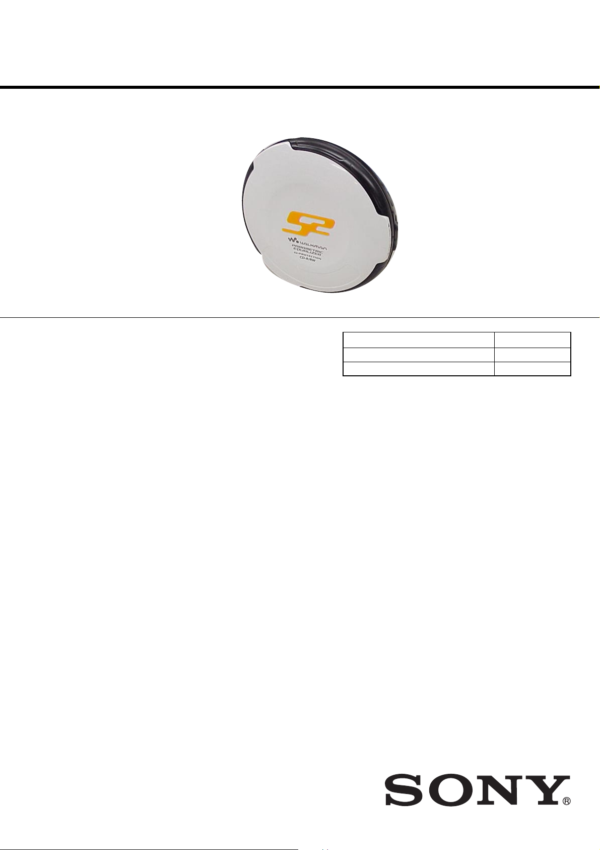
D-NS707F
SERVICE MANUAL
Ver 1.0 2004.04
Manufactured under license from Dolby
Laboratories Licensing Corporation.
SPECIFICATIONS
US Model
Canadian Model
Model Name Using Similar Mechanism D-NE10
CD Mechanism Type CDM-3325ERV2
Optical Pick-up Name DAX-25EV
CD player
System
Compact disc digital audio system
Laser diode properties
Material: GaAlAs
Wav elength: λ = 770 - 800 nm
Emission duration: Continuous
Laser output: Less than 44.6 µW
(This output is the value measured at a distance
of 200 mm from the objective lens surface on the
optical pick-up block with 7 mm aperture.)
D-A conversion
1-bit quartz time-axis control
Frequency response
20 - 20 000 Hz
Output (at 4.5 V input level)
Headphones (stereo minijack)
Approx. 5 mW + Approx. 5 mW at 16 Ω
+1–2
dB (measured by JEITA)
Radio
Frequency range
• 9 kHz step:
TV: 2 - 13 ch
WB (weather band): 1 - 7 ch
FM: 87.5 - 108.0 MHz
AM: 531 - 1 710 kHz
• 10 kHz step:
TV: 2 - 13 ch
WB (weather band): 1 - 7 ch
FM: 87.5 - 108.0 MHz
AM: 530 - 1 710 kHz
Antenna
FM: Headphones/earphones cord antenna
AM: Built-in ferrite bar antenna
General
Power requirements
• LR6 (size AA) batteries: 1.5 V DC 2
• AC power adaptor (DC IN 4.5 V jack):
120 V, 60 Hz
Operating temperature
5°C - 35°C (41°F - 95°F)
Dimensions (w/h/d) (excluding projecting parts
and controls)
Approx. 136 30.5 136 mm (53⁄811⁄453⁄8 in.)
Mass (excluding accessories)
Approx. 276 g (9.8 oz.)
Supplied accessories
•
Headphones
•
CD-ROM (SonicStage)
•
Operating Instructions
•
SonicStage Installation/Operating Guide
Design and specifi cations are subject to change
without notice.
x
x
x
x
x
9-877-798-01
2004D1679-1
© 2004.04
PORTABLE CD PLAYER
Sony Corporation
Personal Audio Company
Published by Sony Engineering Corporation
D-NS707F
This appliance is classified as a CLASS 1 LASER product. The
CLASS 1 LASER PRODUCT MARKING is located on the rear
exterior.
CAUTION
Use of controls or adjustments or performance of procedures
other than those specified herein may result in hazardous radiation
exposure.
Flexible Circuit Board Repairing
•Keep the temperature of soldering iron around 270˚C
during repairing.
• Do not touch the soldering iron on the same conductor of the
circuit board (within 3 times).
• Be careful not to apply force on the conductor when soldering
or unsoldering.
Notes on chip component replacement
•Never reuse a disconnected chip component.
• Notice that the minus side of a tantalum capacitor may be
damaged by heat.
On AC power adaptor
•Use only the AC power adaptor supplied or
recommended in “Accessories (supplied/
optional).” Do not use any other AC power
adaptor. It may cause a malfunction.
Polarity of the plug
TABLE OF CONTENTS
1. SERVICE POSITION .......................................... 3
2. GENERAL ............................................................ 5
3. DISASSEMBLY
3-1. Upper (Lid) Section ......................................................... 6
3-2. Cabinet (Middle) Section ................................................ 7
3-3. MAIN PWB Assy ............................................................ 7
3-4. MAIN Board, CD Mechanism Deck
(CDM-3325ERV2) .......................................................... 8
3-5. Turn Table Motor Assy (M901), Sled Motor Assy (M902),
Optical Pick-up (DAX-25EV) ......................................... 8
4. ELECTRICAL CHECKING ................................ 9
5. DIAGRAMS
5-1. Block Diagram – MAIN Section (1/2) – ......................... 12
Block Diagram – MAIN Section (2/2) – ......................... 13
Block Diagram – TUNER Section – ............................... 14
Block Diagram – POWER Section –............................... 15
5-2. Printed Wiring Board – MAIN Board (Side A) –............ 16
5-3. Printed Wiring Board – MAIN Board (Side B) –............ 17
5-4. Schematic Diagrams – MAIN Board (1/5) –................... 18
5-5. Schematic Diagrams – MAIN Board (2/5) –................... 19
5-6. Schematic Diagrams – MAIN Board (3/5) –................... 20
5-7. Schematic Diagrams – MAIN Board (4/5) –................... 21
5-8. Schematic Diagrams – MAIN Board (5/5) –................... 22
5-9. IC Pin Function Descriptions .......................................... 27
6. EXPLODED VIEWS
6-1. Cabinet Upper.................................................................. 34
6-2. Cabinet Lower ................................................................. 35
6-3. Strap Front ....................................................................... 36
6-4. MAIN PWB Assy ............................................................ 37
6-5. CD Mechanism Deck Section (CDM-3325ERV2).......... 38
Unleaded solder
Boards requiring use of unleaded solder are printed with the leadfree mark (LF) indicating the solder contains no lead.
(Caution: Some printed circuit boards may not come printed with
the lead free mark due to their particular size.)
: LEAD FREE MARK
Unleaded solder has the following characteristics.
• Unleaded solder melts at a temperature about 40°C higher than
ordinary solder.
Ordinary soldering irons can be used but the iron tip has to be
applied to the solder joint for a slightly longer time.
Soldering irons using a temperature regulator should be set to
about 350°C.
Caution: The printed pattern (copper foil) may peel away if the
heated tip is applied for too long, so be careful!
• Strong viscosity
Unleaded solder is more viscous (sticky, less prone to flow)
than ordinary solder so use caution not to let solder bridges
occur such as on IC pins, etc.
• Usable with ordinary solder
It is best to use only unleaded solder but unleaded solder may
also be added to ordinary solder.
7. ELECTRICAL PARTS LIST............................... 39
2
SECTION 1
SERVICING NOTE
D-NS707F
NOTES ON HANDLING THE OPTICAL PICK-UP
BLOCK OR BASE UNIT
The laser diode in the optical pick-up block may suffer electrostatic
breakdown because of the potential difference generated by the
charged electrostatic load, etc. on clothing and the human body.
During repair, pay attention to electrostatic breakdown and also use
the procedure in the printed matter which is included in the repair
parts.
The flexible board is easily damaged and should be handled with
care.
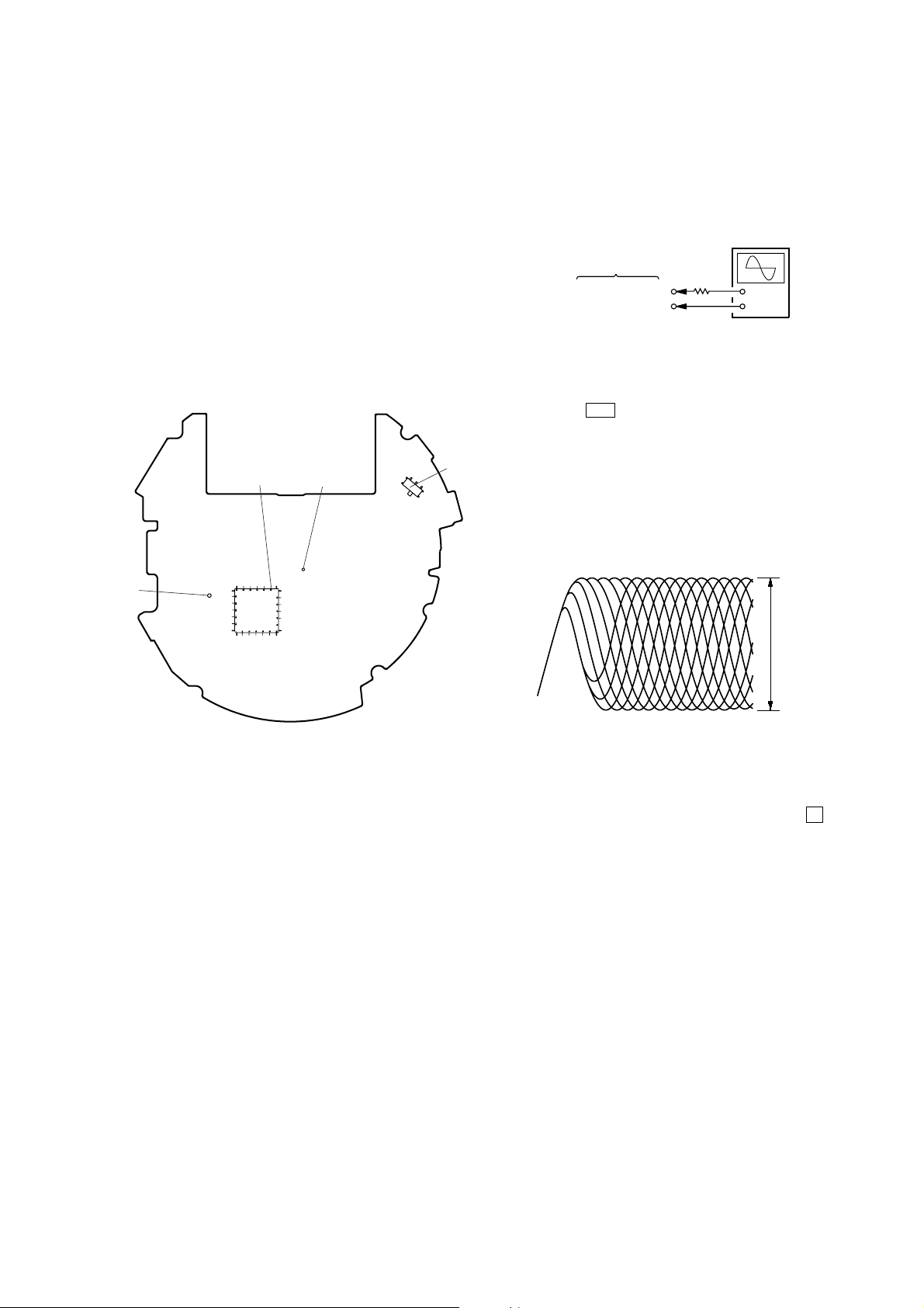
NOTES ON LASER DIODE EMISSION CHECK
The laser beam on this model is concentrated so as to be focused on
the disc reflective surface by the objective lens in the optical pickup block. Therefore, when checking the laser diode emission, observe from more than 30 cm away from the objective lens.
SAFETY-RELATED COMPONENT WARNING!!
COMPONENTS IDENTIFIED BY MARK 0 OR DOTTED LINE WITH
MARK 0 ON THE SCHEMATIC DIAGRAMS AND IN THE PARTS
LIST ARE CRITICAL TO SAFE OPERATION. REPLACE THESE
COMPONENTS WITH SONY PARTS WHOSE PART NUMBERS
APPEAR AS SHOWN IN THIS MANUAL OR IN SUPPLEMENTS
PUBLISHED BY SONY.
BEFORE REPLACING THE OPTICAL PICK-UP BLOCK
Please be sure to check thoroughly the parameters as par the “Optical Pick-Up Block Checking Procedures” (Part No.: 9-960-027-11)
issued separately before replacing the optical pick-up block.
Note and specifications required to check are given below.
• FOK output: IC601 yg pin
When checking FOK, remove the lead wire to disc motor.
• RF signal P-to-P value: 0.45 to 0.65 Vp-p
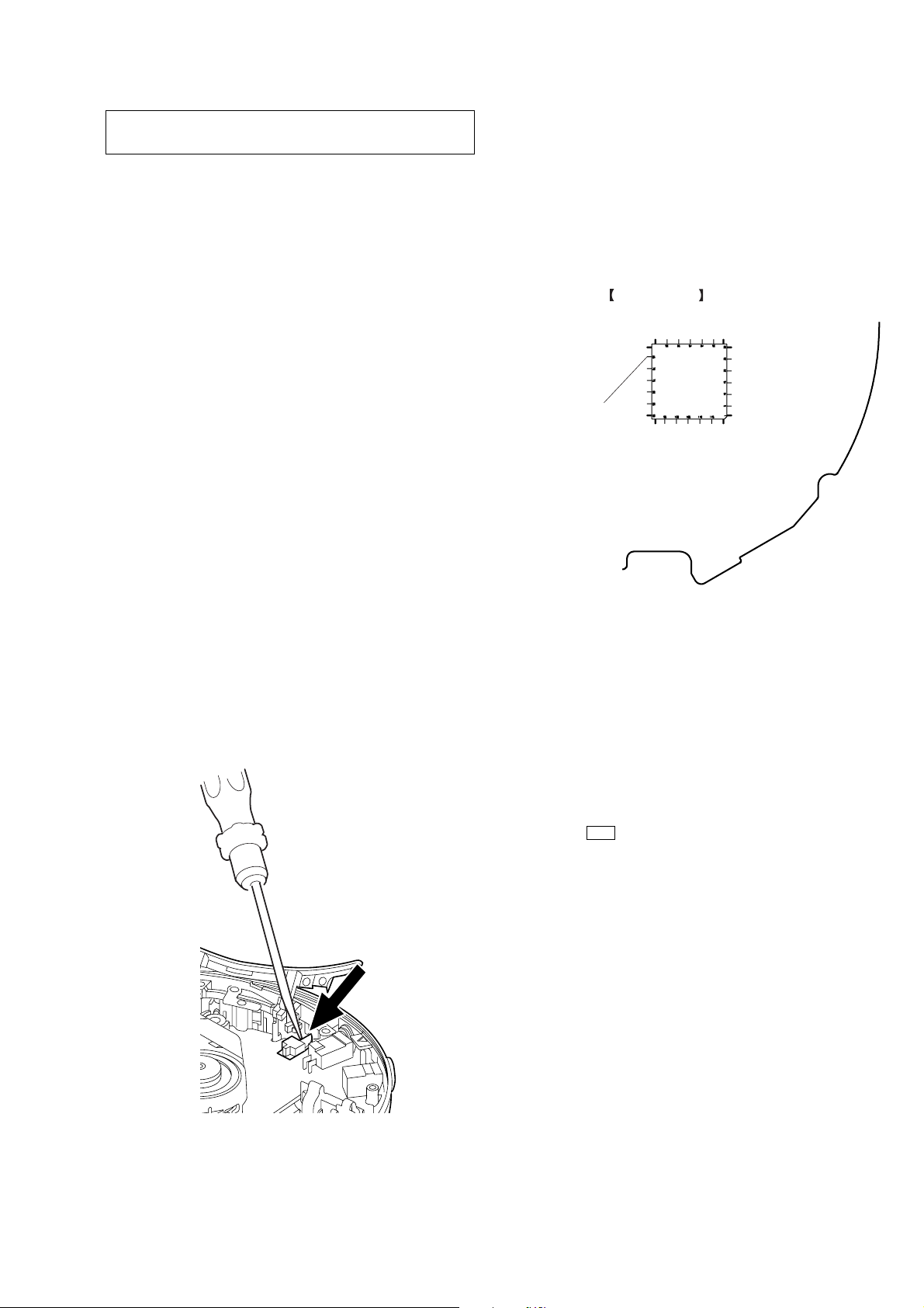
MAIN BOARD (SIDE B)
3160
30
1
120
IC601 FOK output ygpin
61
90
91
ATTENTION AU COMPOSANT AYANT RAPPORT
À LA SÉCURITÉ!
LES COMPOSANTS IDENTIFÉS PAR UNE MARQUE 0 SUR LES
DIAGRAMMES SCHÉMATIQUES ET LA LISTE DES PIÈCES SONT
CRITIQUES POUR LA SÉCURITÉ DE FONCTIONNEMENT. NE
REMPLACER CES COMPOSANTS QUE PAR DES PIÈSES SONY
DONT LES NUMÉROS SONT DONNÉS DANS CE MANUEL OU
DANS LES SUPPÉMENTS PUBLIÉS PAR SONY.
LASER DIODE AND FOCUS SEARCH OPERATION
CHECK
During normal operation of the equipment, emission of the laser
diode is prohibited unless the upper lid is closed while turning ON
the S820.
The following checking method for the laser diode is operable.
• Method:
Emission of the laser diode is visually checked.
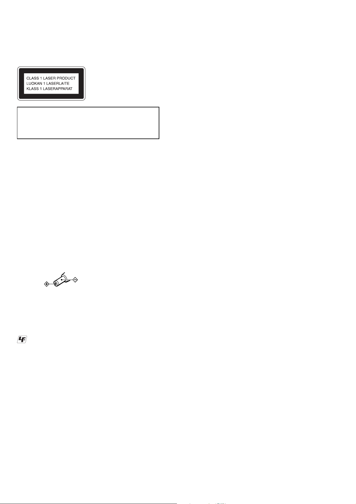
1. Remove the upper lid.
2. With a disc not set, turn on the S820 with a screwdriver having
a thin tip as shown in Fig.1.
3. Press the
u
button.
4. Observing the objective lens, check that the laser diode emits
light.
When the laser diode does not emit light, automatic power control circuit or optical pickup is faulty.
In this operation, the objective lens will move up and down 4
times along with inward motion for the focus search.
Fig. 1 Method to push the S820
3
D-NS707F
SERVICE MODE
The following confirmation can be performed when the Service
Mode is set.
1. How to set the CD Service Mode.
To set the Service Mode, the following method is available.
1) Confirm the set is not powered on.
2) Confirm the following settings.
OPEN/CLOSE detect switch (S820) ................. OFF
Solder Land (TAP833) ...................................... OPEN
[HOLD] switch (S803)........................................ OFF
3) Short the solder land TAP824 (TEST) on the MAIN board.
4) Turn on the main power.
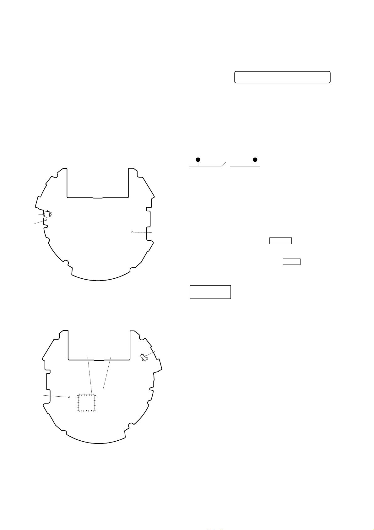
MAIN BOARD(SIDE A)
S820
TAP833
TAP824
MAIN BOARD(SIDE B)
2. Operation when the Service Mode is set.
When the Service Mode becomes active, following messages are
displayed onthe remote control LCD.
Microcomputer
version display
1) Turn off the power.
2) Open the solder land TAP824 (TEST) on the MAIN board.
Note : The solder should be removed clean.
3. How to set the Tuner Service Mode.
To set the tuner Service Mode, the following method is available.
1) Confirm the set is not powered on.
2) Connect a external switch between TJ80 (Tu Test) and TJ81
(Gnd).
TJ80
(TU Test)
3) Slide the switch to connect TJ80 and TJ81 to be shorted.
4) Short the solder land TAP824 (Test).
5) Turn on the main power.
4. Operation when Tuner Service Mode is set.
When the tuner Service Mode becomes active, following the below
procedure.
1) CD microcomputer version display VS010B .
2) Press play key.
3) Display panel show all segments turn on.
4) Then show DTS microcontroller version: 00008
5) Slide the switch to oposite direction to open the connection of
TJ80(Tu test) and TJ81(Gnd).
6) Tuner mode turned on and display panel show :
FM
87.50 MHz
7) After checking complete, turn of the power.
8) Open solder land TAP824 (Test) and remove the external switch.
Note : The solder should be removed clean.
TJ81
(Gnd)
VS010B:
S803
TP746
IC601yg
TP538
4
SECTION 2
32145
GENERAL
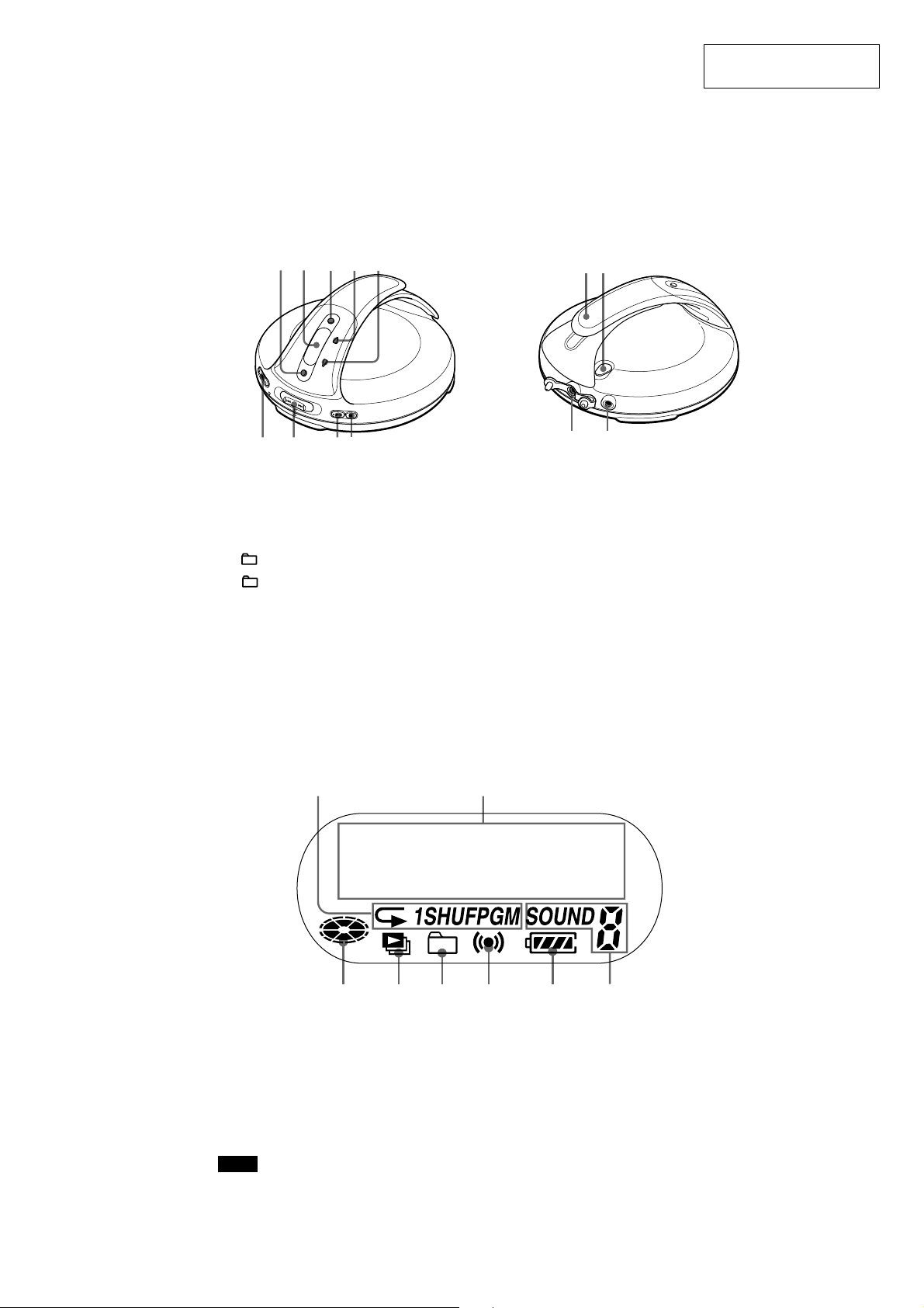
Guide to parts and Controls
0
D-NS707F
This section is extracted
from instruction manual.
qa
RADIO ON/BAND•MEMORY button
1
Display
2
DISPLAY/MENU button
3
4
5
6
VOL (volume) +*/– buttons
.
7
Display
67 89
(group) •TUNE button
(group)
H
•TUNE button
h
/PRESET –, /PRESET + lever
>
H
h
qf qg
qs qd
8
9
0
qa
qs
qd
(play/pause)*/ENTER button
u
(stop)•RADIO OFF button
x
Hand strap
HOLD switch
(headphones) jack
i
DC IN 4.5 V (external power input) jack
* This button has a tactile dot.
qh
Play mode indicator
qf
Character information display
qg
Disc indicator
qh
Play list indicator
qj
Note
Yo u can invert the characters on the display.
qj qk ql w; wa
Group indicator
qk
Timer indicator
ql
w;
Battery indicator
SOUND indicator
wa
5
D-NS707F
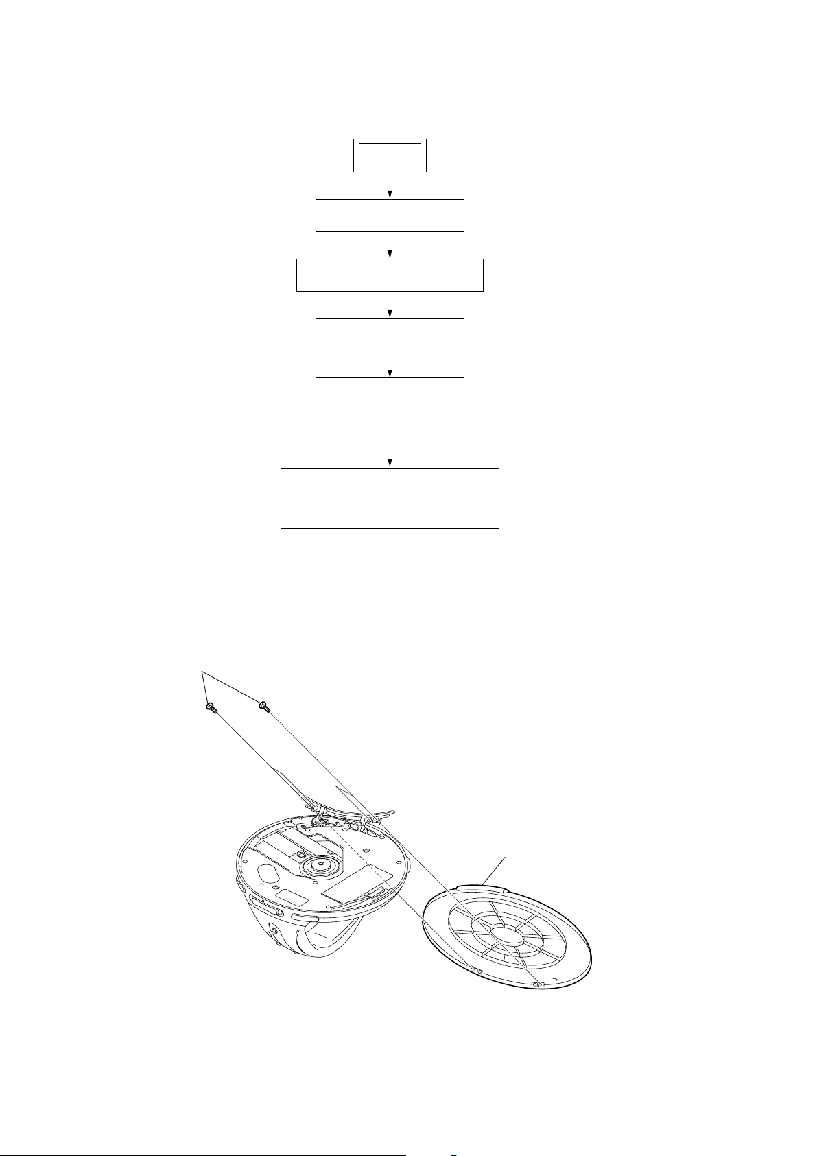
Note: Disassemble the unit in the order as shown below.
SECTION 3
DISASSEMBLY
SET
UPPER (LID) SECTION
CABINET (MIDDLE) SECTION
MAIN PWB ASSY
MAIN BOARD,CD
MECHANISM DECK
(CDM-3325ERV2)
TURN TABLE MOTOR ASSY (M901),
SLED MOTOR ASSY (M902),
OPTICAL PICK-UP (DAX-25EV)
Note: Follow the disassembly procedure in the numerical order given.
3-1. UPPER (LID) SECTION
1
four screws
2
upper lid sub assy
6
s
3-2. CABINET (MIDDLE) SECTION
2
cabinet middle
1
ten screw
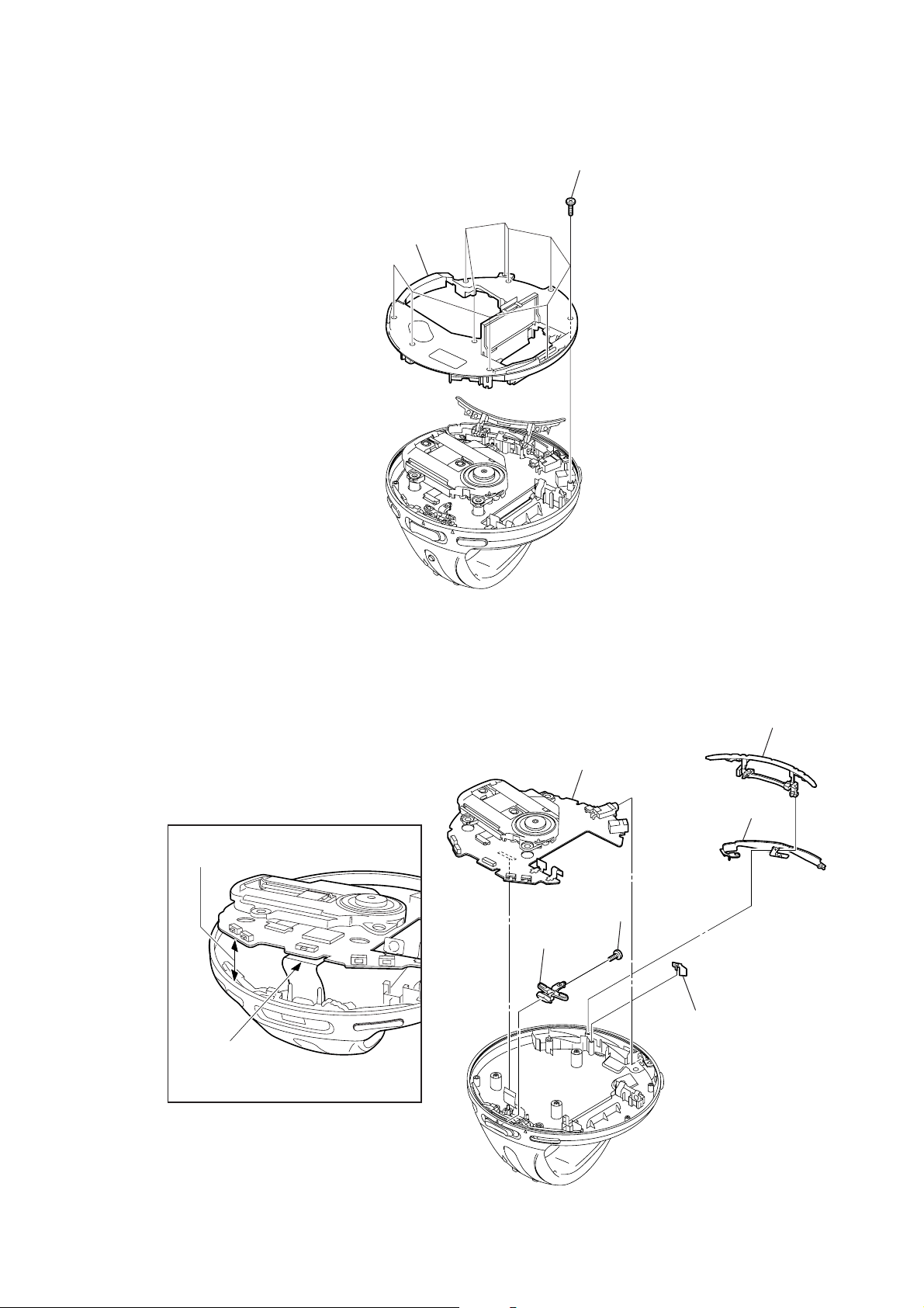
D-NS707F
3-3. MAIN PWB ASSY
Precaution:PWB can not be lifted up
>5cm from back cabinet.
NG
Prohibit:Can not press FPC during
assembly PWB to back cabinet.
6
main pwb assy
5
jog
actuator
4
screw
2
1
hinge support
3
open spring
hinge sliding
7
D-NS707F
)
3-4. MAIN BOARD, CD MECHANISM DECK (CDM-3325ERV2)
4
CD mechanism deck
(CDM-3325ERV2)
3
flexible board
(CN601)
5
com cover
sheet
1
connector (2P
(CN401)
2
connector (4P)
(CN402)
main board
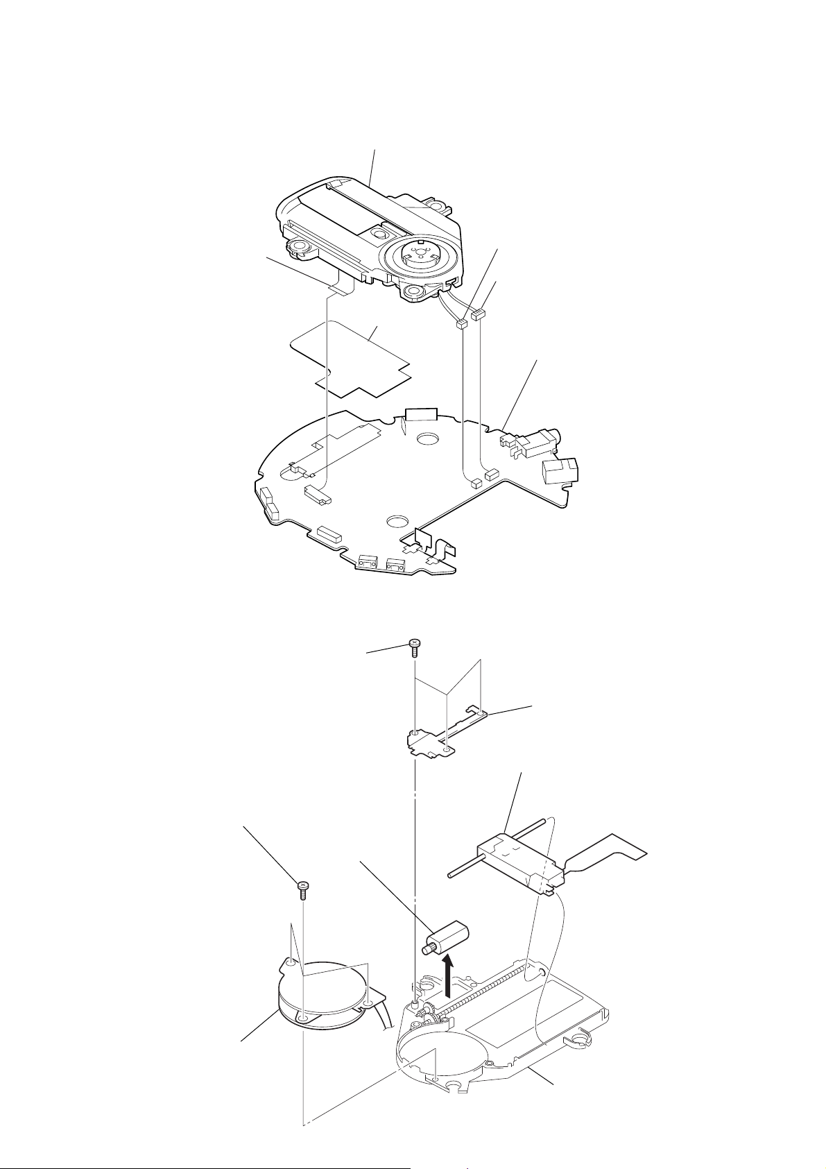
3-5. TURN TABLE MOTOR ASSY (M901), SLED MOTOR ASSY (M902), OPTICAL PICK-UP (DAX-25EV)
1
three screws
5
three screws
(B 1.7
×
(B 1.7
4)
×
4)
3
sled motor assy
(M902)
2
gear cover
4
optical pick-up
(DAX-25EV)
6
turn table motor assy
(M901)
chassis
8
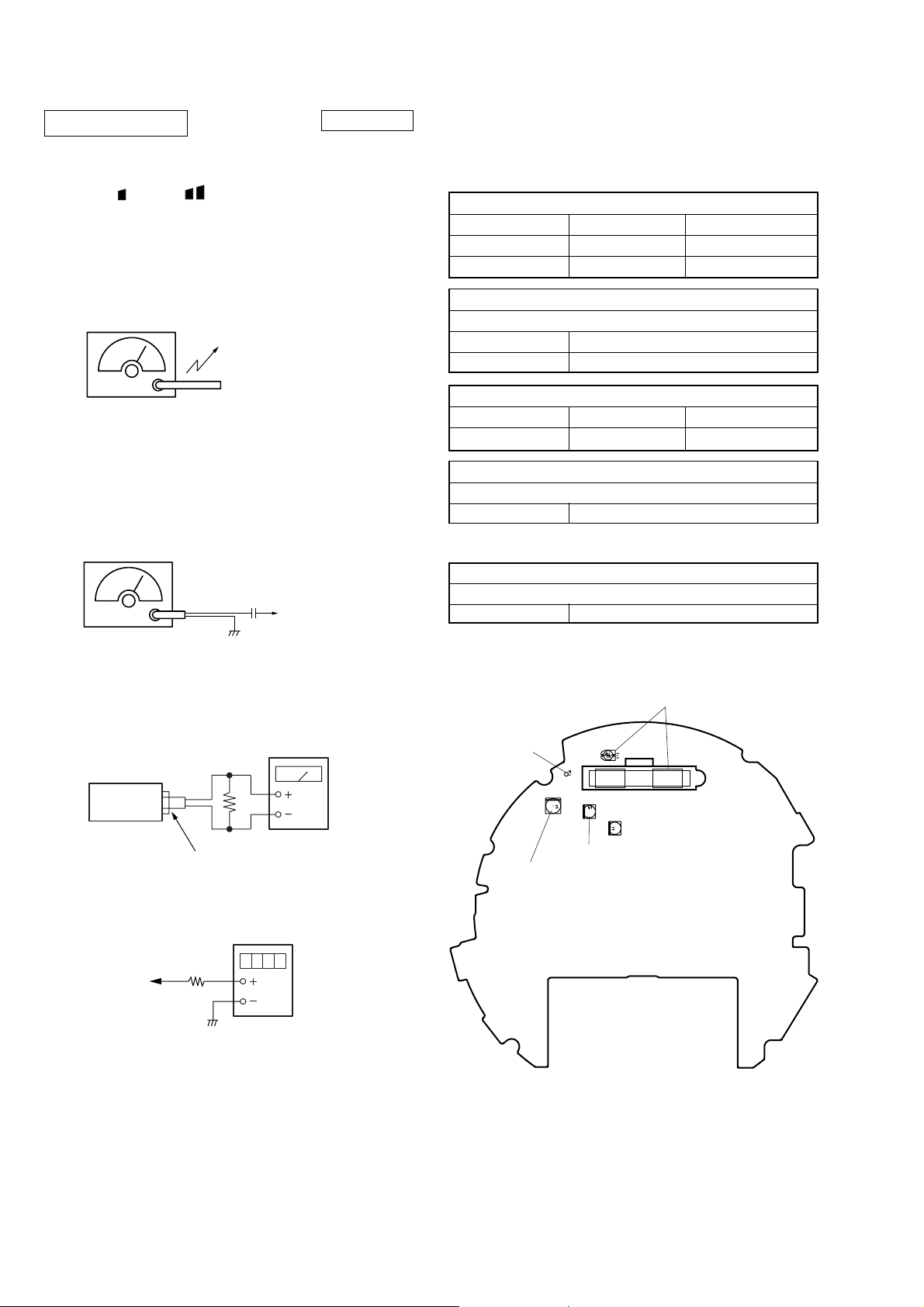
SECTION 4
e
RF level
0.45 to 0.65 Vp-p
ELECTRICAL CHECKING
D-NS707F
The CD section adjustments are done automatically in this set.
In case of operation check, confirm that RF level.
Precautions for Check
1. Perform check in the order given.
2. Use YEDS-18 disc (Part No.: 3-702-101-01) unless otherwise
indicated.
3. Power supply voltage requirement : DC4.5 V in terminals
(J401)
VOLUME button : Minimum
HOLD switch : OFF
Checking Location:
MAIN BOARD(SIDE B)
IC601yg
TP538
S803
RF Level Check
Condition:
• Hold the set in horizontal state.
Connection:
Oscilloscop
(AC range)
MAIN board
Ω
TP746 (RF)
TP538 (AGND)
Procedure:
1. Connect the oscilloscope to the test points TP746 (RF) and
TP538 (AGND) on the MAIN board.
2. Set a disc. (YEDS-18)
3. Press the u button.
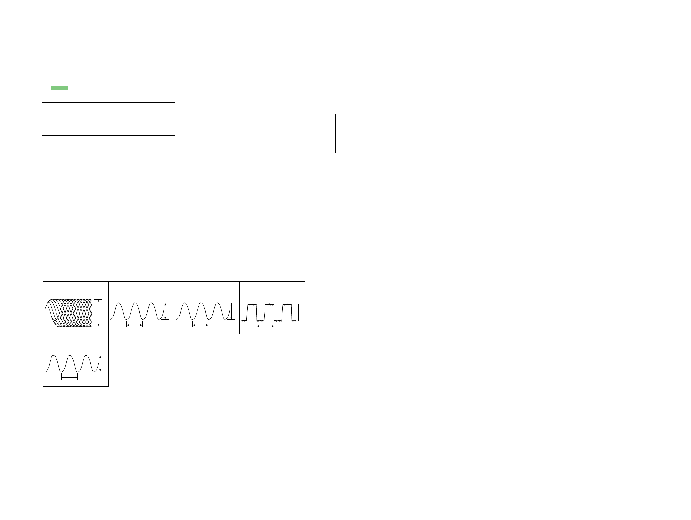
4. Check the oscilloscope waveform is as shown below.
A good eye pattern means that the diamond shape (◊) in the
center of the waveform can be clearly distinguished.
2 k
+
–
RF Signal reference Waveform (Eye Pattern)
VOLT/DIV : 100 mV (With the 10:1 probe in use)
TIME/DIV : 500 ns
TP746
To watch the eye pattern, set the oscilloscope to AC range and
increase the vertical sensitivity of the oscilloscope for easy
watching.
5. Stop revolving of the disc motor by pressing the x button.
9
D-NS707F
N
TUNER SECTION
• Switch Location and mode setting
VOLUME : MAX
BASS
AVLS : OFF
[AM]
BAND: AM
Signal generator
[FM]
BAND : FM
Signal generator
• Connecting levelmeter
or BASS : OFF
AM RF signal
generator
30% amplitude modulation by 400Hz
signal.
Output level : as low as possible
FM RF signal
generator
75kHz(100%) amplitude modulation
by 1kHz signal.
Output level: as low as possible
Put the lead-wire
antenna close to
the set.
0.01µF
FM I
point
0 dB = 1 µV
•Repeat the procedures in each adjustment several times for the
maximum level meter indication.
•The AM tracking adjustments should be finally done by the
trimmer capacitors.
AM FREQUENCY COVERAGE ADJUSTMENT AND CHECK
Adjustment Part Frequency Display
Reading on Digital Voltmeter
L4 530kHz 1.2 ± 0.1V
Confirmation 1710kHz 8.4 ± 0.5V
AM TRACKING ADJUSTMENT
Adjust for a maximum reading on levelmeter
L3 620kHz
CT3 1400kHz
FM FREQUENCY COVERAGE CHECK
Adjustment Part Frequency Display
Reading on Digital Voltmeter
Confirmation 87.5MHz 5.1 ± 0.8V
FM TRACKING ADJUSTMENT
Adjust for a maximum reading levelmeter
L1 98.0MHz
US model only
TV TRACKING ADJUSTMENT
Adjust for a maximum reading on levelmeter
L5 ch10 197.75MHz
Adjustment Location: MAIN board (Side B)
CT3,L3 AM TRACKING adjustment
set
J332 (
i)
• Connecting digital voltmeter
TJ8 (VT)
100k
16 Ω
digital voltmeter
Ω
levelmeter
TJ8(VT)
L4 AM FREQUENCY COVERAGE adjustment
CT3
L3
L1 FM TRACKING adjustment
L5 TV TRACKING adjustment
10
SECTION 5
DIAGRAMS
NOTE FOR PRINTED WIRING BOARDS AND SCHEMATIC DIAGRAMS
D-NS707F
Note on Printed Wiring Board
• X : parts extracted from the component side.
• Y : parts extracted from the conductor side.
• :Pattern from the side which enables seeing.
(The other layers' patterns are not indicated.)
Caution:
Pattern face side: Parts on the pattern face side seen from
(Side B) the pattern face are indicated.
Parts face side: Parts on the parts face side seen from
(Side A) the parts face are indicated.
Note on Schematic Diagram:
• All capacitors are in µF unless otherwise noted. pF: µµF 50 WV
or less are not indicated except for electrolytics and tantalums.
• All resistors are in W and 1/4 W or less unless otherwise
specified.
•%: indicates tolerance.
• C : panel designation.
Note:
The components identified by
mark 0 or dotted line with
mark 0 are critical for safety.
Replace only with part
number specified.
• A : B+ Line.
•Total current is measured with CD installed.
•Power voltage is dc 4.5 V and fed with regulated dc power supply
from DC IN jack.
•Voltages and waveforms are dc with respect to ground in
playback mode.
no mark : CD PLAY
* : Impossible to measure
•Voltages are taken with a VOM (Input impedance 10 MΩ).
Voltage variations may be noted due to normal production
tolerances.
•Waveforms are taken with a oscilloscope.
Voltage variations may be noted due to normal production
tolerances.
• Circled numbers refer to waveforms.
• Signal path.
J : CD PLAY
Note:
Les composants identifiés par une
marque 0 sont critiques pour la
sécurité.
Ne les remplacer que par une
pièce portant le numéro spécifié.
• Waveforms
1
IC601 if RFAC
100mV/DIV, 400ns/DIV
540 mVp-p
5
IC61 ug XIN
500mV/DIV, 10us/DIV
1.4 Vp-p
13.3us
2
IC601 rk XTAO
1V/DIV, 20ns/DIV
3.2 Vp-p
59ns
3
IC801 wk XIN
1V/DIV, 40ns/DIV
3.4 Vp-p
118ns
4
IC403 ef SYNC
1V/DIV, 2us/DIV
5.7us
2.0 Vp-p
1111
D-NS707F
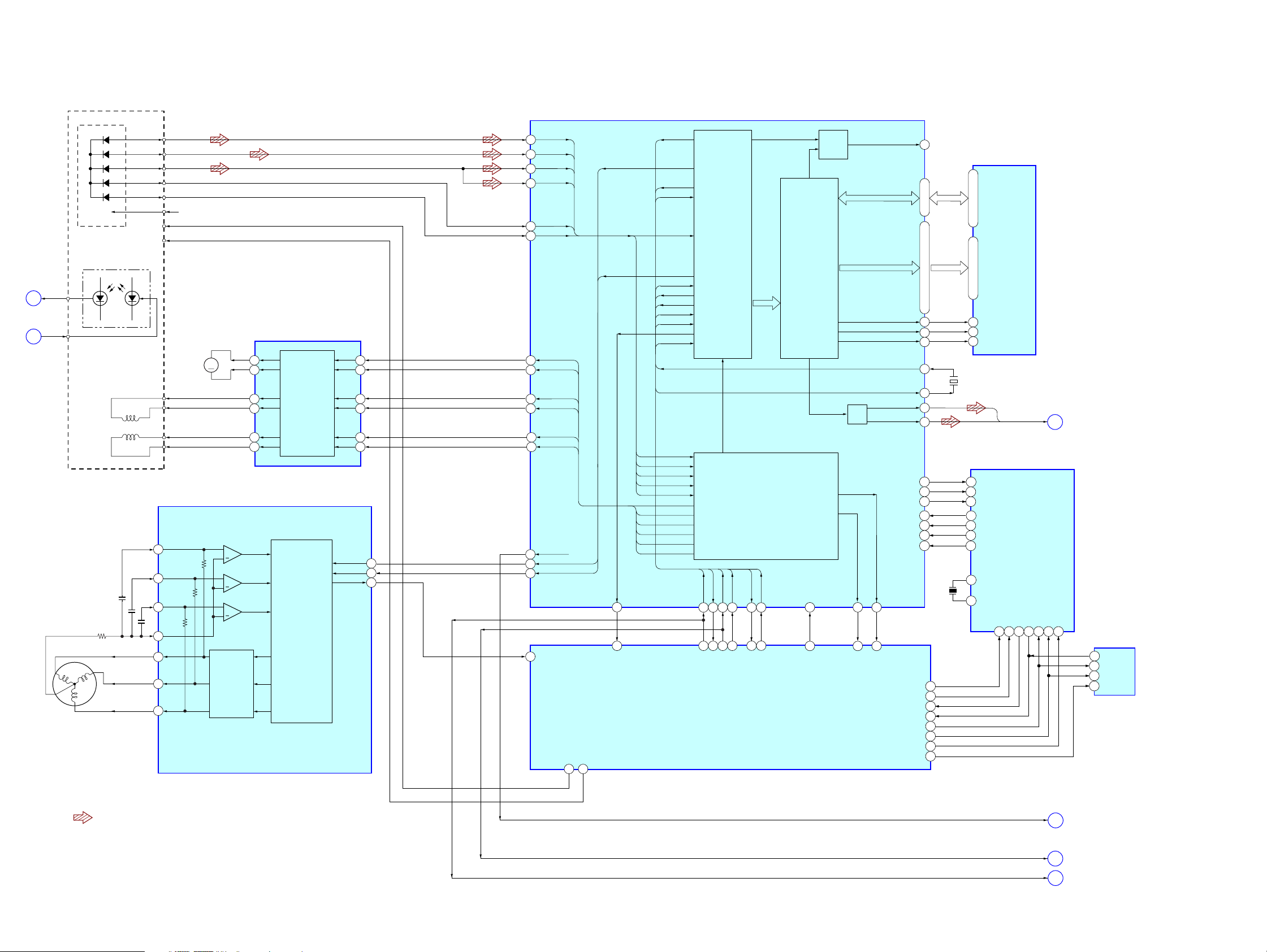
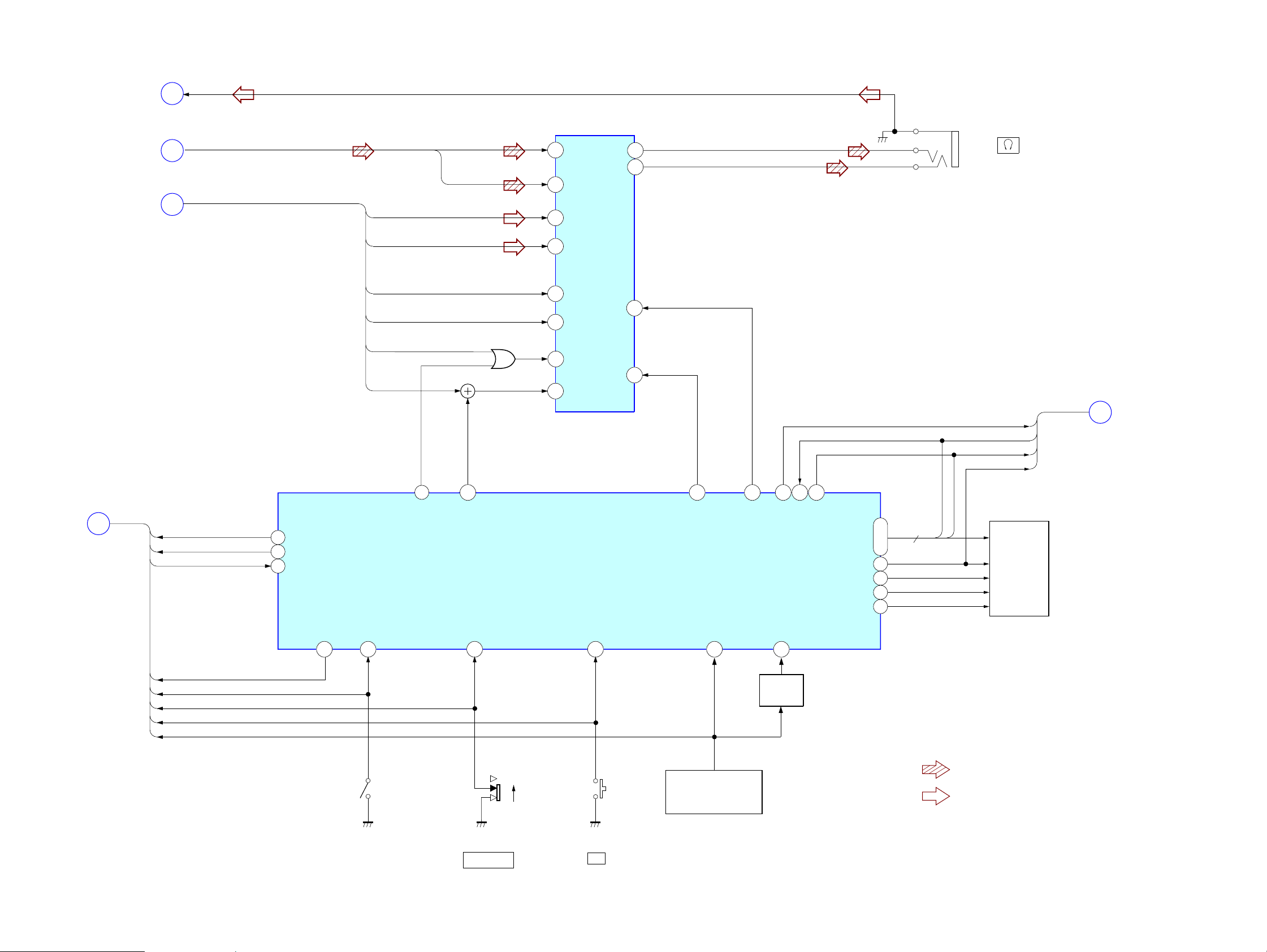
5-1. BLOCK DIAGRAM – MAIN SECTION (1/2) –
DETECTOR
A
(Page 15)
B
(Page 15)
OPTICAL PICK-UP BLOCK
LASER DIODE
PD
LD
(FOCUS)
2-AXIS
DEVICE
(TRACKING)
M902
SPINDLE
MOTOR
V
U
W
A
B
RF
E
F
VCC
DAX-25E
PD
A
B
RF
E
F
VCC3
OPGSW
OPSTB
LD
FOCUS/TRACKING COIL DRIVER
M901
M
SLED
MOTOR
U1
79
V1
78
W1
77
COM
80
U
2
V
4
W
6
+
+
+
MOTOR
DRIVER
FO1
52
RO1
50
FO3
44
RO3
42
FO2
42
RO2
40
IC403 (1/3)
SLED MOTOR DRIVER
CONTROLLER,
H BRIDGE DRIVER
IC403 (2/3)
SPINDLE MOTOR DRIVER
CONTROL
CIRCUIT
FI1
RI1
FI3
RI3
FI2
RI2
APWM
XBRK
IC601
RF AMP,
DIGITAL SIGNAL PROCESSOR,
DIGITAL SERVO PROCESSOR,
D-RAM CONTROLLER
A
92
B
91
RFDC
88
RFAC
84
E
89
F
90
SFDR
56
55
60
59
58
57
73
70
FG
74
100
104
103
102
SRDR
99
FFDR
96
FRDR
95
TFDR
98
TRDR
97
C176
MDP
MDS
SCOR
27
FG_I
10
SCOR_I
HG_XSTB_O
HG_GUP_O
12
13
WFCK
MDS
XTAO
XTAI
RFAC
XSOE
SENS
R4M
XLAT
CLOK
SCOR
SDTO
RFDC
SFDR
SRDR
FFDR
FRDR
TFDR
TRDR
SIGNAL
PROCESSOR
BLOCK
MDP
E
F
B
A
SDTO
SENS
858887838486
MSDTO0_O
IC801 (1/3)
SYSTEM CONTROLLER
CLOK
XLAT
232021
MSCK_O
MSDTI0_I
XLAT0_O
R8M
32
28
SERVO
BLOCK
XSOE
2422
XIN
XSOE_O
MEMORY
CONTROLLER,
BASS BOOST
BLOCK
XRST
28
4
XRST_O
DIGITAL
OUT
FOK
GFS
LPF
GFS
69
53
GFS_I
DOUT
D0-D3
A0-A10
XRAS
XWE
XCAS
XTAI
XTAO
AOUT1
AOUT2
PCMD_O
LRCK_O
BCK_O
PCMD_I
LRCK_I
BCK_I
XRDE
FOK
65
52
FOKI
AT3_MP3_V_O
WAKEUP_K_O
REQ_I
SDIN_I
SDOUT_O
SDCLK_O
SDXLAT_O
EEP_CS_O
62
4, 3, 6, 5
116 – 113, 17 – 15, 13 – 11, 117
1
2
9
47
48
51
56
108
106
110
109
107
111
18
X701
22MHz
60
66
11
20
19
18
17
67
D0 – D3A0 – A10
2, 3, 24, 25
9 – 12, 15 – 19, 21, 8
5
XRAS
4
XWE
23
XCAS
X601
16.9344MHz
4
PCMD
1
LRCK
2
BCK
15
PI0
14
PI2
13
PI3
12
PF4
29
EXTAL
30
XTAL
IC603
D-RAM
AOUTL,
AOUTR
IC701
MP3 DECODER
PF0
NRST
PF3
33
34
37
40
PC1
41
D
(Page 13)
PC0
PC2
38
42
PC3
4
3
2
1
IC803
EEPROM
DO
DI
XSK
XCS
• SIGNAL PATH
: CD PLAY
SYNC
MSCK
MSDTO
E
F
G
(Page 15)
(Page 15)
(Page 15)
1212
BLOCK DIAGRAM – MAIN SECTION (2/2) –
FMANT
H
(Page 14)
CD L, CD R
D
(Page 12)
CD L
CD R
IC332
HEADPHONE AMP
32
36
CD LIN
CD RIN
LOUT
ROUT
D-NS707F
J332
7
5
K
(Page 14)
I
(Page 14)
CDON
DTS RST
TUON
55 CDON_O
59 DTS_RST_O
68 TUON_I
TU L
TU R
VOL CTRL
BST SW
TU MUTE
TU BEEP
7
AMUTE_O
CD MUTE
6
BEEP_O
D335
33
TU LIN
35
TU RIN
14
VOL CTL
INSW
44
26
BST SW
1
MUTE
PWRSW
BEEP3
IC801 (2/3)
SYSTEM CONTROLLER
31
77
HP_PWRSW
56
AUD_SEL
21
22
DTS_SDTI
DTS_SDTO
23
AD0-7
DTS_SCK
LCD_A0
XRD_O
XWR_O
LCD-XRST_O
44
51
69
71
72
73
DTSSDTO
DTSSDTI
DTSSCK
A0
AD6
|
8
AD7
LCD UNIT
J
(Page 14)
ACK2SCK
LID OPEN
HOLD
ADKEY2
ADKEY1
ACK2SCK
16
(OPEN/CLOSE)
LID-SW_I
37
S820
HOLD_I
40
S810
> HOLD
ON
OFF
97
S801
x
AD-KEY2
S802 - 805
FUNCTION
KEY
1313
AD-KEY1
96
JOGKEY_I
36
Q801
SWITCH
• SIGNAL PATH
: CD PLAY
: FM

D-NS707F
BLOCK DIAGRAM – TUNER SECTION –
(Page 13)
RF/IF AMP, FM/AM DET, FM MPX
FM/TV MIX
TV
OSCFMOSC
1/2
AM
OSC
AM MIX
BPF
REF
REF
REF
TV RF OUT
30
FM RF OUT
29
TV RF IN
1
FM RF IN
2
TV FM OSC
24
AM OSC
25
AM BYPASS
28
AM RF IN
27
VT
Q152
FMANT
H
FL1/FL2
IC1
1/8
1/16
FM MIX
AM MIX
CF2
4 8
CF1
5
10
FM IF IN
AM IF IN
AGC
FM
DET
LEVEL
DET
AM
DET
IF
SW
DET OUT
AF
FM
MPX
MPX IN
L OUT
R OUT
LPF1
12
13
16
15
14
Q1
TU L
TU R
I
(Page 13)
(Page 13)
(Page 15)
FM/AM/TV
PW SW
MODE1
OSC OUT
23
IC61
ACK CD-O
54
ACKCD
73
DST RST
TUNER CONTROLLER
XIN
XOUT
RESET_I
75
74
X61
75kHz
T81
DDCON
3.2V
Q86
OSC
VCPU
Q89
Q84,85
VT
41
TV-L ON_O
65
EQ(DO1)_O
40
NC
AD DC REF
57
45
VCPU
1.4VREF
XTU TEST_I
SUBEY1_2
38
37
TU ON
ADKEY2
CD ON_I
TU ON_O
42
39
ADKEY1
CD ON
BATT_I
KEY_I
44
43
AD I HIDC
AD I BATT
71
HIDC_I
AM IN
TU HOLD_I
51
HOLD
K
L
MODE2
21
22
53
52
BAND CTRL 1_O
BAND CTRL 2_O
EEP CS_O
SCK-I-CDU
SDO-O-CDU
32
48
47
46427
1
2
3
DI
CS
SK
IF REQ
20
Q71
IFREQ_O
SDI-I-CDU
CS_O
A0_O
26
DO
IF COUNT
19
BUFF
6461
60
IFIN_I
+B ON/OFF_O
MONO_O 55
TUBEEP_O
PWM OUT_O 50
BST SW_O 58
TUMUTE_O
49
62
TUBEEP
VOL CTRL
BST SW
TUMUTE
DTS SDTO
DTS SDTI
DTS SCK
• SIGNAL PATH
XCS
A0
J
(Page 13)
: FM
IC62
EEPROM
1414
 Loading...