

Sony DNF-007, DNF-0070 Service manual
D-NF007/NF0070
SERVICE MANUAL
Ver. 1.1 2005.11
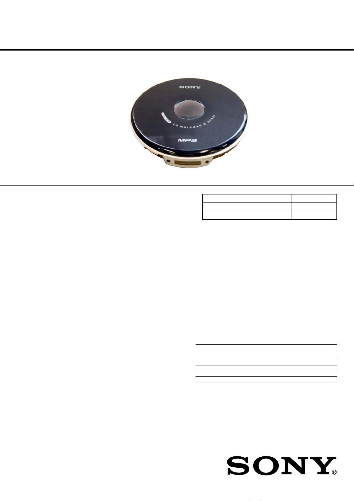
Photo : D-NF007
SPECIFICATIONS
Canadian Model
AEP Model
D-NF007
E Model
D-NF007/NF0070
Australian Model
D-NF007
Model Name Using Similar Mechanism D-FJ003
CD Mechanism Type CDM-3525A
Optical Pick-up Name DAX-25E
CD player
System: Compact disc digital audio system
Laser diode properties:
Emission duration: Continuous
Laser output: Less than 44.6 µW (This output is the value measured at a
distance of 200 mm from the objective lens surface on the optical pick-up
block with 7 mm aperture.)
Radio
Frequency range
• Canadian and Latin American models
9 kHz step:
FM: 87.5 - 108 MHz
AM: 531 - 1 710 kHz
10 kHz step:
FM: 87.5 - 108 MHz
AM: 530 - 1 710 kHz
• Other models
9 kHz step:
FM: 87.5 - 108 MHz
AM: 531 - 1 602 kHz
10 kHz step:
FM: 87.5 - 108 MHz
AM: 530 - 1 710 kHz
Antennas
FM: Headphones cord antenna
AM: Built-in ferrite bar antenna
General
Power requirements:
•Two LR6 (size AA) batteries: 1.5 V DC × 2
• AC power adaptor (DC IN 4.5 V jack):
220 V, 50 Hz (Model for China)
120 V, 60 Hz (Model for Mexico)
Dimensions (w/h/d) (without projecting parts and controls):
Approx. 139.8 × 28.8 × 139.8 mm (5 5⁄8 × 1 3⁄16 × 5 5⁄8 in.)
Mass (excluding accessories):
Approx. 219 g (7.8 oz.)
Operating temperature: 5°C - 35°C (41°F - 95°F)
MPEG Layer-3 audio coding technology and patents licensed from
Fraunhofer IIS and Thomson.
Design and specifications are subject to change without notice.
Supplied accessories
AC power adaptor (1) (not supplied with the USA model)
Headphones (1)
Battery life* (approx. hours)
(When the CD player is used on a flat and stable place.)
Playing time varies depending on how the CD player is used.
When using two Sony alkaline batteries LR6 (SG)
(produced in Japan)
G-PROTECTION G-on G-off
Audio CD 16 11
MP3 CD (Recorded at 128 kbps) 23 23
RADIO ON 35
* Measured value by the standard of JEITA (Japan Electronics and
Information Technology Industries Association).
Design and specifications are subject to change without notice.
FM/AM PORTABLE CD PLAYER
9-879-827-02
2005K02-1
© 2005.11
Sony Corporation
Personal Audio Division
Published by Sony Engineering Corporation
D-NF007/NF0070
TABLE OF CONTENTS
1. SERVICING NOTES ................................................ 3
2. GENERAL ................................................................... 3
3. DISASSEMBLY
3-1. Disassembly Flow ........................................................... 4
3-2. Upper Lid Assy, Cabinet (Middle) Assy,
Cabinet (Lower) Assy...................................................... 4
3-3. Optical Pick-Up (CDM-3525A), Main Board ................. 5
4. ELECTRICAL ADJUSTMENT ............................. 6
5. DIAGRAMS
5-1. Block Diagram – CD/Power Section –........................... 10
5-2. Block Diagram – Tuner Section – .................................. 11
5-3. Printed Wiring Board – Main Board (Side A) – ............. 12
5-4. Printed Wiring Board – Main Board (Side B) – ............. 13
5-5. Schematic Diagram – Main Board (1/3) – ..................... 14
5-6. Schematic Diagram – Main Board (2/3) – ..................... 15
5-7. Schematic Diagram – Main Board (3/3) – ..................... 16
5-8. IC Pin Function Description ............................................ 20
6. EXPLODED VIEWS ................................................. 23
7. ELECTRICAL PARTS LIST .................................. 24
Notes on chip component replacement
• Never reuse a disconnected chip component.
• Notice that the minus side of a tantalum capacitor may be
damaged by heat.
Flexible Circuit Board Repairing
• Keep the temperature of the soldering iron around 270 ˚C
during repairing.
• Do not touch the soldering iron on the same conductor of the
circuit board (within 3 times).
• Be careful not to apply force on the conductor when soldering
or unsoldering.
CAUTION
Use of controls or adjustments or performance of procedures
other than those specified herein may result in hazardous radiation
exposure.
UNLEADED SOLDER
Boards requiring use of unleaded solder are printed with the leadfree mark (LF) indicating the solder contains no lead.
(Caution: Some printed circuit boards may not come printed with
the lead free mark due to their particular size.)
: LEAD FREE MARK
Unleaded solder has the following characteristics.
• Unleaded solder melts at a temperature about 40°C higher than
ordinary solder.
Ordinary soldering irons can be used but the iron tip has to be
applied to the solder joint for a slightly longer time.
Soldering irons using a temperature regulator should be set to
about 350°C.
Caution: The printed pattern (copper foil) may peel away if
the heated tip is applied for too long, so be careful!
• Strong viscosity
Unleaded solder is more viscous (sticky, less prone to flow)
than ordinary solder so use caution not to let solder bridges
occur such as on IC pins, etc.
• Usable with ordinary solder
It is best to use only unleaded solder but unleaded solder may
also be added to ordinary solder.
SAFETY-RELATED COMPONENT WARNING!!
COMPONENTS IDENTIFIED BY MARK 0 OR DOTTED LINE
WITH MARK 0 ON THE SCHEMATIC DIAGRAMS AND IN
THE PARTS LIST ARE CRITICAL TO SAFE OPERATION.
REPLACE THESE COMPONENTS WITH SONY PARTS WHOSE
PART NUMBERS APPEAR AS SHOWN IN THIS MANUAL OR
IN SUPPLEMENTS PUBLISHED BY SONY.
2
ATTENTION AU COMPOSANT AYANT RAPPORT
À LA SÉCURITÉ!
LES COMPOSANTS IDENTIFIÉS PAR UNE MARQUE 0 SUR LES
DIAGRAMMES SCHÉMATIQUES ET LA LISTE DES PIÈCES
SONT CRITIQUES POUR LA SÉCURITÉ DE FONCTIONNEMENT.
NE REMPLACER CES COMPOSANTS QUE PAR DES PIÈCES
SONY DONT LES NUMÉROS SONT DONNÉS DANS CE MANUEL
OU DANS LES SUPPLÉMENTS PUBLIÉS PAR SONY.
SECTION 1
SERVICING NOTES
D-NF007/NF0070
NOTES ON HANDLING THE OPTICAL PICK-UP
BLOCK OR BASE UNIT
The laser diode in the optical pick-up block may suffer electrostatic
break-down because of the potential difference generated by the
charged electrostatic load, etc. on clothing and the human body.
During repair, pay attention to electrostatic break-down and also
use the procedure in the printed matter which is included in the
repair parts.
The flexible board is easily damaged and should be handled with
care.
NOTES ON LASER DIODE EMISSION CHECK
The laser beam on this model is concentrated so as to be focused on
the disc reflective surface by the objective lens in the optical pickup block. Therefore, when checking the laser diode emission,
observe from more than 30 cm away from the objective lens.
LASER DIODE AND FOCUS SEARCH OPERATION
CHECK
During normal operation of the equipment, emission of the laser
diode is prohibited unless the upper lid is closed while turning ON
the S811. (push switch type)
The following checking method for the laser diode is operable.
• Method:
Emission of the laser diode is visually checked.
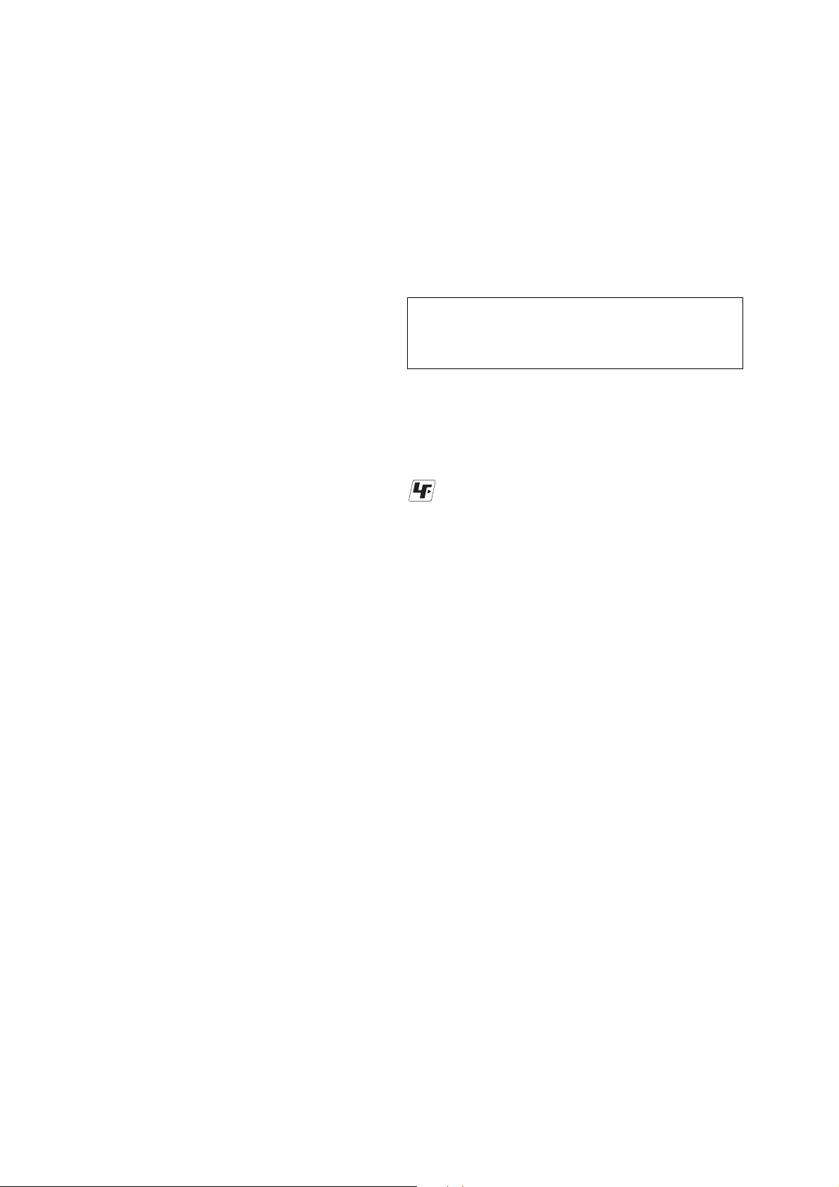
1. Open the upper lid.
2. With a disc not set, turn on the S811 with a screwdriver having
a thin tip as shown in Fig.1.
3. Press the u button.
4. Observing the objective lens, check that the laser diode emits
light.
When the laser diode does not emit light, automatic power
control circuit or optical pick-up is faulty.
In this operation, the objective lens will move up and down 2
times along with inward motion for the focus search.
S811
LOCATING THE CONTROLS
SOUND/AVLS
i (headphones) jack
P MODE/
VOL +*/–
OPEN
HOLD (rear)
RADIO ON/BAND
* The button has a tactile dot.
Headphones
MONO
LOCAL
PRESET
Band
Track number/Preset number
Playing time/Frequency
SECTION 2
GENERAL
Display
PRESET LOCAL MONO
Fig. 1 Method to push the S811
This section is extracted from
instruction manual.
DC IN 4.5 V
to an AC outlet
AC power adaptor
./>•
TUNE –/+
u*(play/pause)/ENTER
x (stop)•RADIO OFF
GROUP
MP3 indicator
Play mode
Remaining battery power
Group indicator
Sound mode
(group) –/+ •
3
D-NF007/NF0070
• This set can be disassembled in the order shown below.
3-1. DISASSEMBLY FLOW
3-2. UPPER LID ASSY, CABINET (MIDDLE) ASSY, CABINET (LOWER) ASSY
(Page 4)
3-3. OPTICAL PICK-UP (CDM-3525A),
MAIN BOARD
(Page 5)
SECTION 3
DISASSEMBLY
SET
Note: Follow the disassembly procedure in the numerical order given.
3-2. UPPER LID ASSY, CABINET (MIDDLE) ASSY, CABINET (LOWER) ASSY
4
screw
upper lid assy
3
five screws
5
two claws
cabinet (middle) assy
2
1
open
6
three claws
cabinet (lower) assy
4
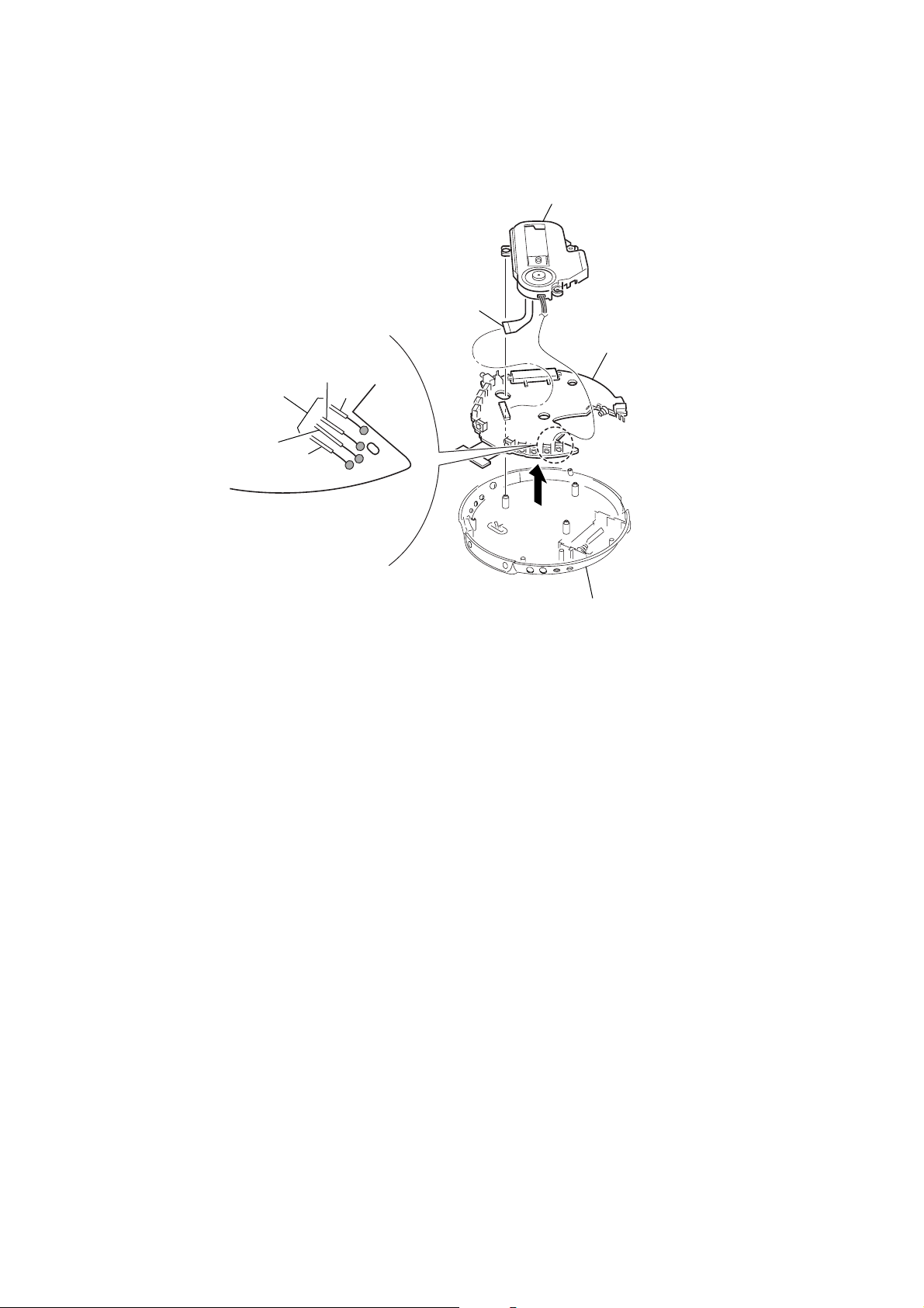
3-3. OPTICAL PICK-UP (CDM-3525A), MAIN BOARD
A
1
CN501
3
Unsolder four lead wires
4
optical pick-up CDM-3525
5
MAIN board
D-NF007/NF0070
to optical pick-up
BLK
RED
MAIN board (side A)
GRY
ORG
2
cabinet (lower) assy
5
D-NF007/NF0070
Ver. 1.1
SECTION 4
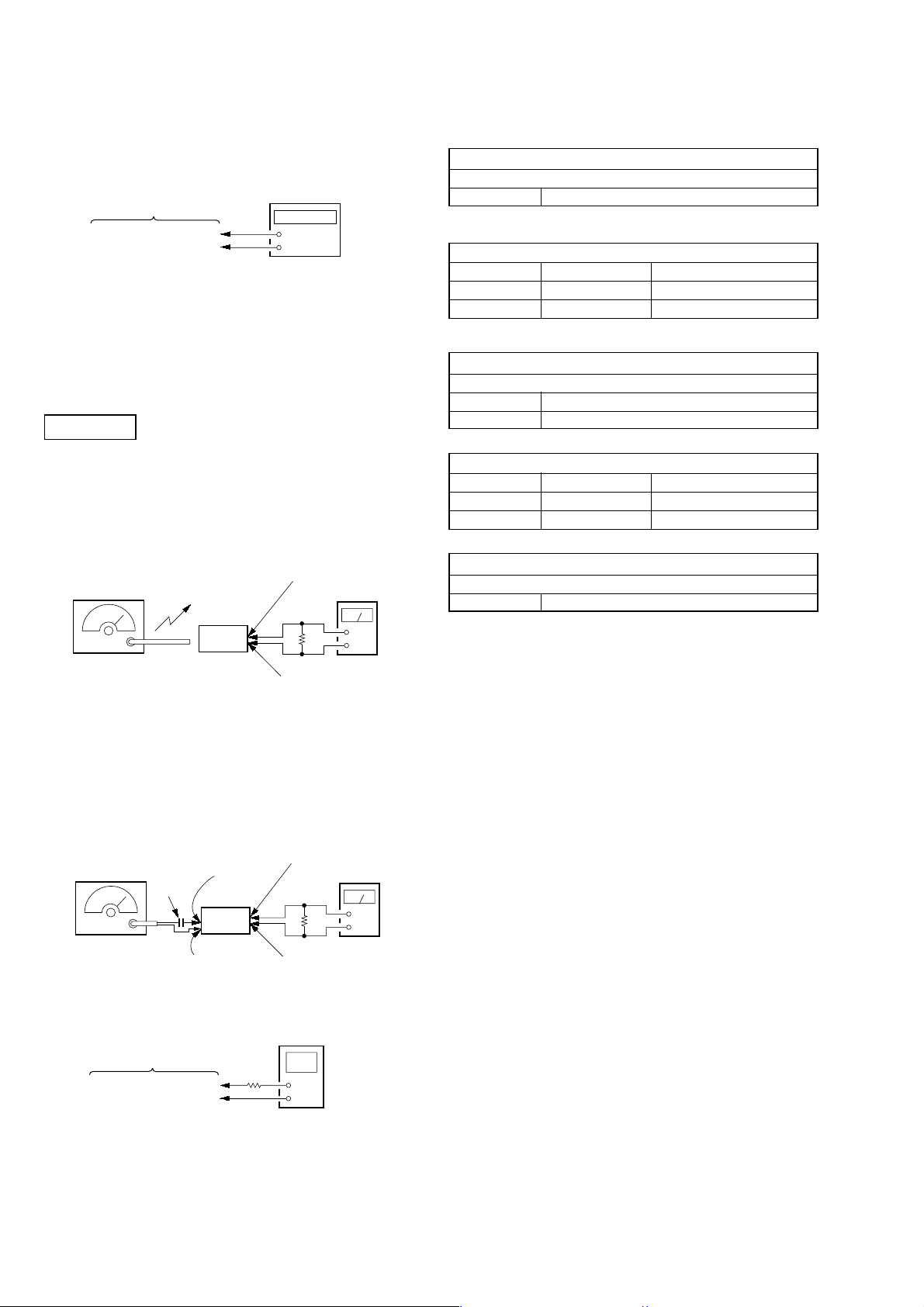
ELECTRICAL ADJUSTMENTS
[TUNER SECTION]
CLOCK SHIFT ADJUSTMENT
Connection:
MAIN board
TP471 (SIFT)
TP005 (RFGND (A)) or
TP003 (RFGND (B))
frequency counter
+
–
Adjusting Procedure:
1. Connect the frequency counter to TP471 (SIFT) and TP005
(RFGND (A)) or TP003 (RFGND (B)) on the MAIN board.
2. Set the AM 621 kHz (9kHz step model) or AM 620 kHz
(10kHz step model)
3. Adjust the RV471 so that the reading of frequency counter is
180 ± 1 kHz.
0 dB=1 µV
[AM]
Setting:
Function: RADIO
Band: AM
AVLS: OFF
MAIN board
AM RF signal
generator
30% amplitude
modulation by
400 Hz signal
Output level:
as low as possible
Put the lead-wire
antenna close to
the set.
TP012 (TU_L) or
TP014 (TU_R)
32
Ω
set
MAIN board
TP005 (RFGND (A)) or
TP003 (RFGND (B))
level meter
+
–
( ): 9kHz step model
AM IF ADJUSTMENT
Adjust for a maximum reading on level meter
T002 620 (621) kHz
( ): 9kHz step model
AM FREQUENCY COVERAGE CONFIRMATION
Adjustment Part Frequency Display Reading in Digital Voltmeter
Confirmation 530 (531) kHz 0.8 ± 0.5 V
Confirmation 1,710 (1,602) kHz 7.2 (6.8) ± 1.0 V
( ): 9kHz step model
AM TRACKING ADJUSTMENT
Adjust for a maximum reading on level meter
T001 620 (621) kHz
CT001 1,400 (1,404) kHz
FM FREQUENCY COVERAGE ADJUSTMENT
Adjustment Part Frequency Display Reading in Digital Voltmeter
Confirmation 87.5 MHz 2.8 ± 1.0 V
L004 108 MHz 8.0 ± 1.0 V
FM TRACKING ADJUSTMENT
Adjust for a maximum reading on level meter
L003 98 MHz
Adjustment and Connecting Location: MAIN board
(See page 7)
[FM]
Setting:
Function: RADIO
Band: FM
AVLS: OFF
MAIN board
TP012 (TU_L) or
TP014 (TU_R)
level meter
32
Ω
MAIN board
TP005 (RFGND (A)) or
TP003 (RFGND (B))
digital voltmeter
Ω
+
–
FM RF signal
generator
0.01 µF
33.75 kHz frequency
deviation by 1 kHz
signal
Output level:
as low as possible
TP005 (RFGND (A)) or
TP003 (RFGND (B))
TP005 (RFGND (A)) or
MAIN board
TP006 (VT)
MAIN board
TP002 (RF (A)) or
TP001 (RF (B))
set
MAIN board
TP003 (RFGND (B))
100 k
• Repeat the procedures in each adjustment several times, and
the tracking adjustments should be finally done by the trimmer
capacitors.
6
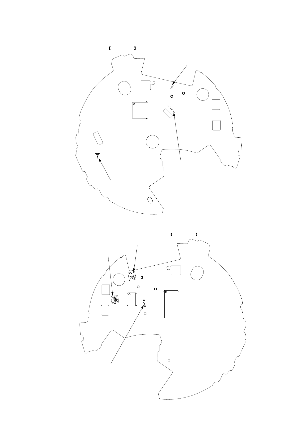
Adjustment and Connecting Location:
D-NF007/NF0070
(SIDE A)MAIN BOARD
CT001:
AM Tracking Adjustment
RV471:
Clock Shift Adjustment
T002:
AM IF Adjustment
TP005
80
1
IC601
20
21
(RFGND(A))
61
60
41
40
T001:
AM Tracking Adjustment
TP001
(RF(B))
L003:
FM Tracking Adjustment
MAIN BOARD
(SIDE B)
TP002
T001
(RF(A))
TP003
(RFGND(B))
1
IC001
15
30
16
TP012
(TUL)
TP006
(VT)
L004:
FM Frequency Coverage Adjustment
TP014
(TUR)
1
25
TP471
(SIFT)
50
IC602
26
7
D-NF007/NF0070
R601
1
0
)
Ver. 1.1
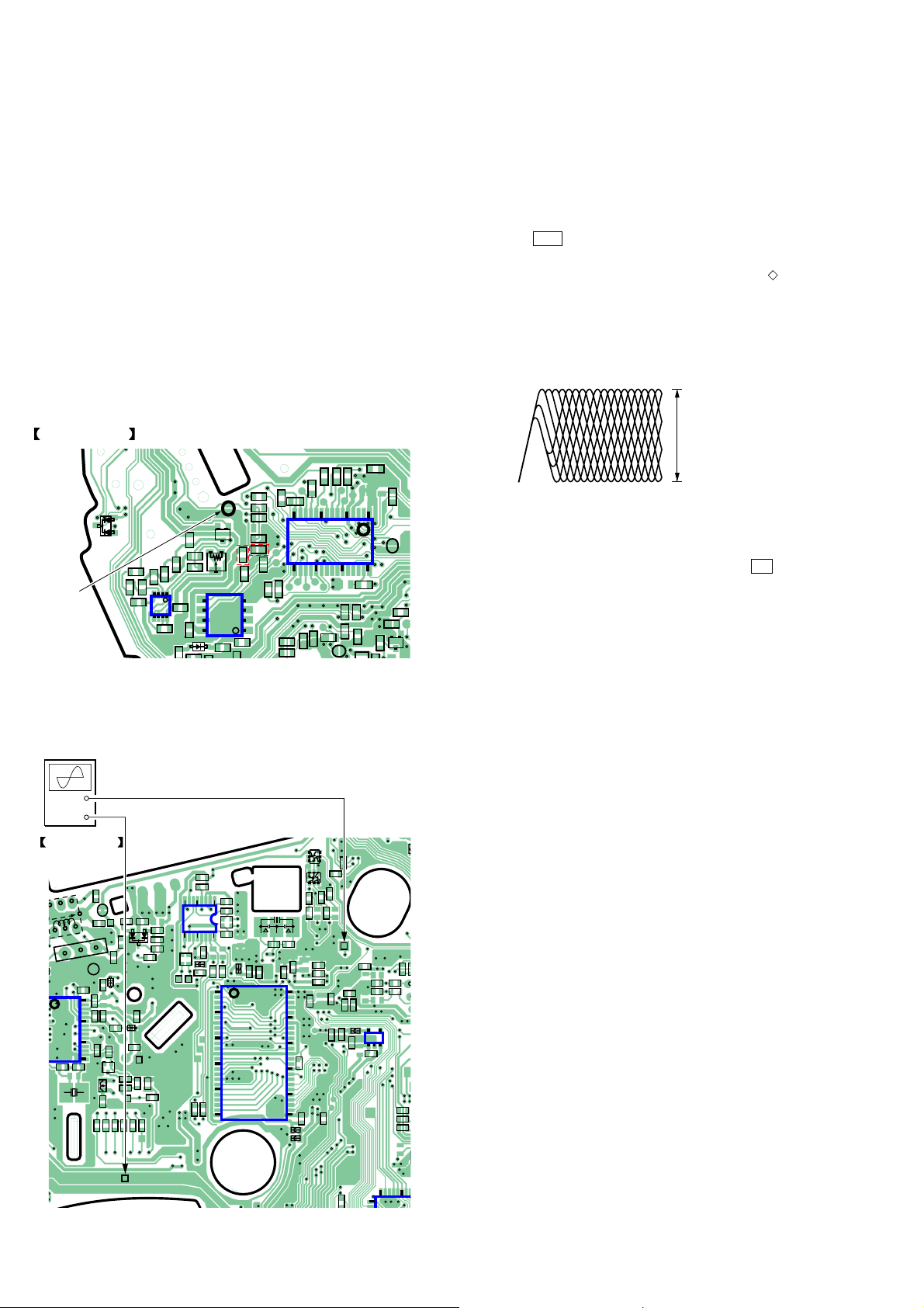
[CD SECTION]
The CD section adjustments are done automatically in this set.
Adjusting Procedure:
1. Perform check in the order given.
2. Use YEDS-18 disc (Part No: 3-702-101-01) unless otherwise
indicated.
3. Power supply voltage requirement :DC4.5 V in DC IN jack.
(J401)
VOLUME button : Minimum
HOLD switch :OFF
Focus bias Check
Condition:
• Hold the set in horizontal state.
Connection:
D871
(SIDE A)
R472
R475
C472
R474
4
C478
5
R411
C474
1
IC471
8
D004
C471
C473
021
SL801
OPEN
R477
(EXCEPT AEP)
R476
R473
C805
Q475
RV471
5
IC802
8
ECB
C040
4
R020
(AEP)
R824
R1015
R1014
R821
R872
R1016
15
16
R1010
IC1001
C001
R871
R873
R826
R828
R812
R808
R804
R844
R843
1
8
MAIN BOARD
SL801(OPEN)
C880
R1011
R1012
C814
R874
R1003
R1019
C812
C806
R1017
1
Procedure:
1. Make a solder bridge to short SL801 (OPEN) on the MAIN
board side A.
2. Connect the oscilloscope to the test point TP604 (RF) and
TP406 (M-GND) on the MAIN board side B.
3. Set a disc. (YEDS-18)
4. Press the u button.
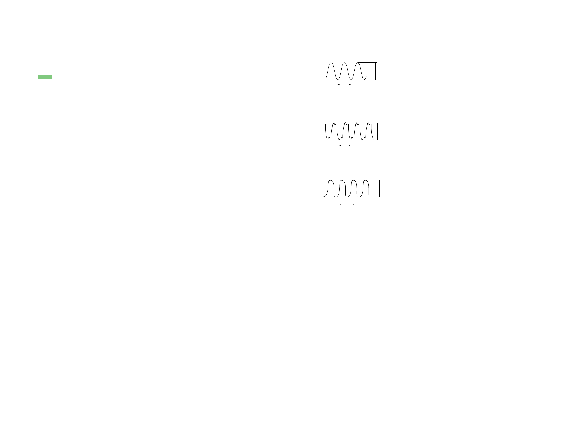
5. Check the oscilloscope waveform is as shown below.
A good eye pattern means that the diamond shape (
) in the
center of the waveform can be clearly distinguished.
RF Signal reference Waveform (Eye Pattern)
VOLT/DIV : 500 mV (With the 10 : 1 probe in use
TIME/DIV : 500ns
RF level
±
0.2 Vp-p
1.2
R1018
To watch the eye pattern, set the oscilloscope to AC range and
increase the vertical sensitivity of the oscilloscope for easy
watch-ing.
SL871
30
6. Stop revolving of the disc motor by pressing the x button.
7. SL801 is opened by taking the solder bridge.
R876
C874
ECB
C877
Q804
2
oscilloscope
(AC range)
+
–
MAIN BOARD
(SIDE B)
1
TAP001
C014
TP002
RF(A)
FL001
TAP003
RF GND(B)
C023
30
IC001
16
5
C043C045
X001
TP406
M-GND
TP604(RF)
TP406(M-GND)
NATURAL
GREEN
RED
C022
R004
C003
C002
R001
C024
C005
D001
R002
C006
D002
C011
C020
C018
R007
C021
C037
R109
G
D
S
L005
C046
R013
R018
TP012
TUL
C102
D003
C109
TP013
GND
C031
R014
C035
C032
R016
TP006
VT
R220
R024
R012
R011
8
9
RB901
TP014
TUR
IC901
R906
R902
R901
R1008
C910
R1009
FB901
Q102
C301
Q101
R303
C620
50
TP604
C635
R617
C627
FB604
FB605
R204
R203
R103
C109
C209
RF
C631
R626
R621
C626
R632
R606
C612
C606
C605
FB606
C632
C633
C634
R627
1
C905
C906
X601
R902
C907
16
R905
R618 R622
FB601
C638
R904
C624
1
IC602
25
26
1004
IC603
5
1
R630
41
FB201
R620
R615
C615
R613
C609
4
3
R605
R604
R603
IC
40
8
SECTION 5
DIAGRAMS
D-NF007/NF0070
• Note for Printed Wiring Boards and Schematic Diagrams
Note on Printed Wiring Boards.
• X : parts extracted from the component side.
• Y : parts extracted from the conductor side.
• a : Through hole.
• f : internal component
• : Pattern from the side which enables seeing.
(The other layers' patterns are not indicated.)
Caution:
Pattern face side: Parts on the pattern face side seen from
(Side B) the pattern face are indicated.
Parts face side: Parts on the parts face side seen from
(Side A) the parts face are indicated.
• Abbreviation
3AEP : UK model
8E19 : Philippines model
AUS : Australian model
CND : Canadian model
E19 : Singapore model
EE : East European model
Note on Schematic Diagrams.
• All capacitors are in µF unless otherwise noted. (p: pF)
50 WV or less are not indicated except for electrolytics
and tantalums.
• All resistors are in Ω and 1/
specified.
• f : internal tolerance.
• C : panel designation.
Note:
The components identified
by mark 0 or dotted line
with mark 0 are critical for
safety.
Replace only with part
number specified.
• A : B+ Line.
• H : adjustment for repair.
• Power voltage is dc 3 V and fed with regulated dc power
supply from battery terminal.
•Voltages and waveforms are dc with respect to ground
under no-signal (detuned) conditions.
no mark : CD PLAY
( ) : FM
[ ] : AM
•Voltages are taken with a VOM (Input impedance 10 MΩ).
Voltage variations may be noted due to normal production tolerances.
•Waveforms are taken with a oscilloscope.
Voltage variations may be noted due to normal production tolerances.
• Circled numbers refer to waveforms.
• Signal path.
J : CD PLAY
F : FM
f : AM
• Abbreviation
3AEP : UK model
8E19 : Philippines model
AUS : Australian model
CND : Canadian model
E19 : Singapore model
EE : East European model
4
W or less unless otherwise
Note:
Les composants identifiés
par une marque 0 sont
critiques pour la sécurité.
Ne les remplacer que par une
piéce portant le numéro
spécifié.
•Waverforms
IC601 ya XO (CD play mode)
1
0.5 V/DIV, 20 ns/DIV
IC801 yd XOUT4M
2
(CD play mode)
1 V/DIV, 50 ns/DIV
IC001 qg X O (RADIO mode)
3
1 V/DIV, 5 µs/DIV
59 ns
1.8 Vp-p
3.5 Vp-p
126 ns
1.6 Vp-p
13.75 µs
D-NF007/NF0070
99
 Loading...