

Sony DNE-336-CK, DNE-331-CK Service manual

D-NE331CK/NE336CK
SERVICE MANUAL
Ver. 1.1 2006.06
SPECIFICATIONS
US Model
D-NE336CK
E Model
D-NE331CK
Model Name Using Similar Mechanism NEW
CD Mechanism Type CDM-3325ERV2
Optical Pick-up Name DAX-25EV
System
Compact disc digital audio system
Laser diode properties
Emission duration: Continuous
Laser output: Less than 44.6 µW
(This output is the value measured at a distance
of 200 mm from the objective lens surface on the
optical pick-up block with 7 mm aperture.)
D-A conversion
1-bit quartz time-axis control
Frequency response
20 - 20 000 Hz
Output
Headphones (stereo minijack)
Approx. 15 mW + Approx. 15 mW at 16 Ω
Power requirements
• LR6 (size AA) battery: 1.5 V DC × 1
• AC power adaptor (DC IN 3 V jack):
120 V, 60 Hz (NE331CK: MX)
100 - 240 V, 50/60 Hz (NE331CK: E33)
Operating temperature
5°C - 35°C (41°F - 95°F)
+1
dB (measured by JEITA)
−2
Dimensions (w/h/d) (excluding projecting parts
and controls)
Approx. 137.8× 31.1× 137.8 mm
1
(5
⁄2× 1 1⁄4× 5 1⁄2 in.)
Mass (excluding accessories)
Approx. 191 g (6.8 oz.)
Supplied Accessories
AC power adaptor (NE331CK)
Earphones
Rotary commander
Car battery cord
Car connecting pack
Velcro tapes for the CD player
Velcro tape for the rotary commander
Operating instructions
AC plug adaptor (NE331CK: E33)
US and foreign patents licensed from Dolby
Laboratories.
MPEG Layer-3 audio coding technology and patents
licensed from Fraunhofer IIS and Thomson.
Design and specifications are subject to change
without notice.
"ATTERYLIFE
7HENUSINGA3ONYALKALINEBATTERY,2
3'PRODUCEDIN*APAN
!UDIO#$
!42!##$
-0#$
-EASUREDVALUEUSINGTHE*%)4!*APAN
%LECTRONICSAND)NFORMATION4ECHNOLOGY
)NDUSTRIES!SSOCIATION
0LAYINGTIMESHOWNISAPPROXIMATEHOURSWHEN
YOUUSETHEPLAYERONAmATANDSTABLESURFACEAND
h0/7%23!6%vISSETTOh/.v
4HISVALUEVARIESDEPENDINGONHOWTHEPLAYER
ISUSED
2ECORDEDATKBPS
2ECORDEDATKBPS
• Abbreviation
'02/4%#4)/.
hv hv
E33: 100 – 240V AC area in E model
MX : Mexican model
9-887-071-02
2006F05-1
© 2006.06
PORTABLE CD PLAYER
Sony Corporation
Personal Audio Division
Published by Sony Techno Create Corporation
D-NE331CK/NE336CK
.OTESONTHE!#POWERADAPTOR
s $ISCONNECTALLPOWERSOURCESWHENTHEPLAYERIS
NOTTOBEUSEDFORALONGTIME
s 5SEONLYTHE!#POWERADAPTORSUPPLIED)FYOUR
PLAYERISNOTSUPPLIEDWITHAN!#POWERADAPTOR
USEAN!#%('!#POWERADAPTOR$ONOT
USEANYOTHER!#POWERADAPTOR)TMAYCAUSEA
MALFUNCTION
. OTAVAILABLEIN!USTRALIAANDSOMEOTHER
REGIONS!SKYOURDEALERFORDETAILED
INFORMATION
0OLARITYOFTHEPLUG
s $ONOTTOUCHTHE!#POWERADAPTORWITHWET
HANDS
s #ONNECTTHE!#POWERADAPTORTOANEASILY
ACCESSIBLE!#OUTLET3HOULDYOUNOTICEAN
ABNORMALITYINTHE!#POWERADAPTORDISCONNECTIT
FROMTHE!#OUTLETIMMEDIATELY
Note on the car battery cord
The 3 V DC plug supplied with car battery
cord conforms to the proposed standards
of the Japan Electronics and Information
Technology Industries Association (JEITA).
Do not connect it to other players.
Polarity of the plug
(JEITA standards)
Notes on chip component replacement
• Never reuse a disconnected chip component.
• Notice that the minus side of a tantalum capacitor may be
damaged by heat.
TABLE OF CONTENTS
1. SERVICING NOTES ............................................... 3
2. GENERAL ................................................................... 4
3. DISASSEMBLY
3-1. Disassembly Flow ........................................................... 5
3-2. Cabinet Lower Sub Assy, Upper Lid Sub Assy ............... 5
3-3. MAIN Board, Optical Pick-Up Assy
(CDM-3325ERV2) .......................................................... 6
3-4. SWITCH Board ............................................................... 6
4. DIAGRAMS
4-1. Schematic Diagram – MAIN Board (1/3) – .................... 9
4-2. Schematic Diagram – MAIN Board (2/3) – .................... 10
4-3. Schematic Diagram – MAIN Board (3/3) – .................... 11
4-4. Printed Wiring Board
– MAIN Board (Component Side) – ............................... 12
4-5. Printed Wiring Board
– MAIN Board (Conductor Side) – ................................. 13
4-6. Printed Wiring Board – SWITCH Board – ..................... 14
4-7. Schematic Diagram – SWITCH Board – ........................ 15
5. EXPLODED VIEWS
5-1. Upper Lid Section ........................................................... 21
5-2. Cabinet Lower Section .................................................... 22
5-3. Optical Pick-Up Section (CDM-3325ERV2) .................. 23
6. ELECTRICAL PARTS LIST................................ 24
Flexible Circuit Board Repairing
• Keep the temperature of the soldering iron around 270 ˚C
during repairing.
• Do not touch the soldering iron on the same conductor of the
circuit board (within 3 times).
• Be careful not to apply force on the conductor when soldering
or unsoldering.
CAUTION
Use of controls or adjustments or performance of procedures
other than those specified herein may result in hazardous radiation
exposure.
SAFETY-RELATED COMPONENT WARNING!!
COMPONENTS IDENTIFIED BY MARK 0 OR DOTTED LINE
WITH MARK 0 ON THE SCHEMATIC DIAGRAMS AND IN
THE PARTS LIST ARE CRITICAL TO SAFE OPERATION.
REPLACE THESE COMPONENTS WITH SONY PARTS WHOSE
PART NUMBERS APPEAR AS SHOWN IN THIS MANUAL OR
IN SUPPLEMENTS PUBLISHED BY SONY.
2
SECTION 1
SERVICING NOTES
D-NE331CK/NE336CK
NOTES ON HANDLING THE OPTICAL PICK-UP
BLOCK OR BASE UNIT
The laser diode in the optical pick-up block may suffer electrostatic
break-down because of the potential difference generated by the
charged electrostatic load, etc. on clothing and the human body.
During repair, pay attention to electrostatic break-down and also
use the procedure in the printed matter which is included in the
repair parts.
The flexible board is easily damaged and should be handled with
care.
NOTES ON LASER DIODE EMISSION CHECK
The laser beam on this model is concentrated so as to be focused on
the disc reflective surface by the objective lens in the optical pickup block. Therefore, when checking the laser diode emission,
observe from more than 30 cm away from the objective lens.
UNLEADED SOLDER
Boards requiring use of unleaded solder are printed with the leadfree mark (LF) indicating the solder contains no lead.
(Caution: Some printed circuit boards may not come printed with
the lead free mark due to their particular size)
: LEAD FREE MARK
Unleaded solder has the following characteristics.
• Unleaded solder melts at a temperature about 40 °C higher
than ordinary solder.
Ordinary soldering irons can be used but the iron tip has to be
applied to the solder joint for a slightly longer time.
Soldering irons using a temperature regulator should be set to
about 350 °C.
Caution: The printed pattern (copper foil) may peel away if
the heated tip is applied for too long, so be careful!
• Strong viscosity
Unleaded solder is more viscou-s (sticky, less prone to flow)
than ordinary solder so use caution not to let solder bridges
occur such as on IC pins, etc.
• Usable with ordinary solder
It is best to use only unleaded solder but unleaded solder may
also be added to ordinary solder.
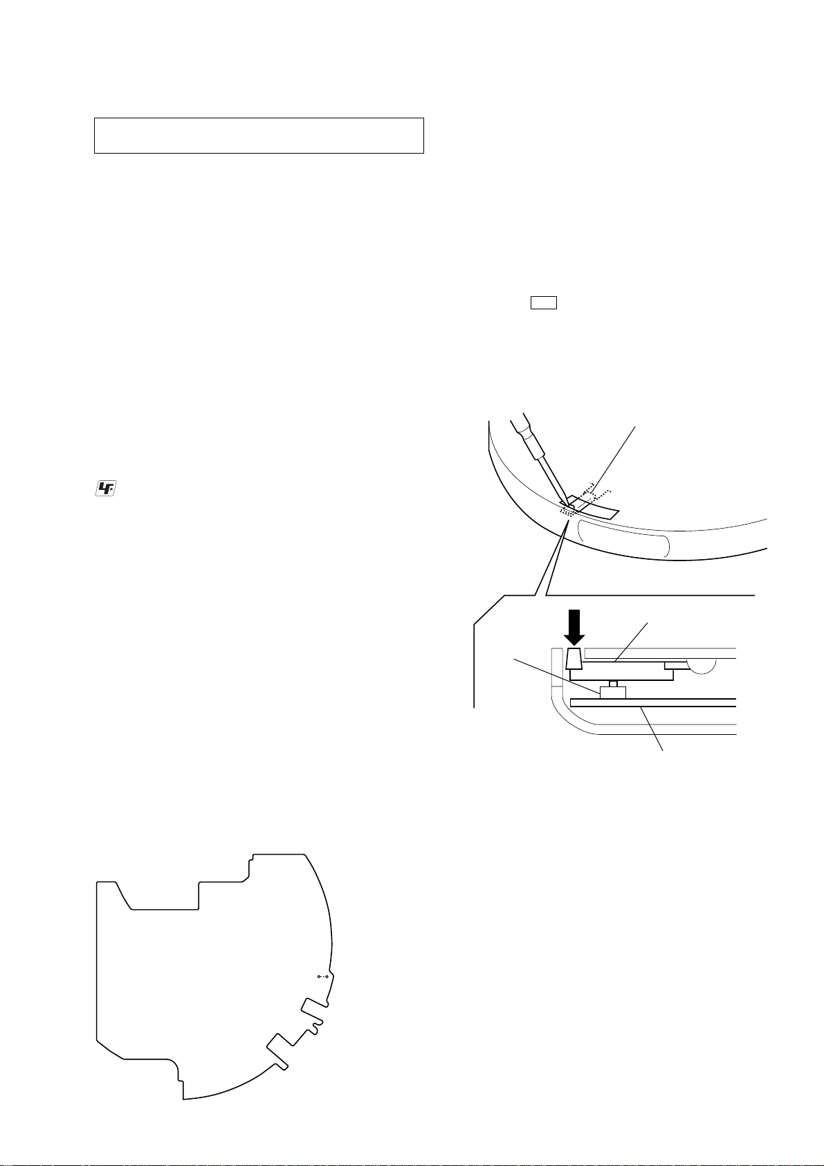
LASER DIODE AND FOCUS SEARCH OPERATION
CHECK
During normal operation of the equipment, emission of the laser
diode is prohibited unless the upper lid is closed while turning on
the S801. (push switch type)
The following checking method for the laser diode is operable.
• Method:
Emission of the laser diode is visually checked.
1. Open the upper lid.
2. With a disc not set, turn on the S801 with a screwdriver having
a thin tip as shown in Fig.1.
3. Press the u button.
4. Observing the objective lens, check that the laser diode emits
light.
When the laser diode does not emit light, automatic power
control circuit or optical pick-up is faulty.
In this operation, the objective lens will move up and down 2
times along with inward motion for the focus search.
lever (detector)
lever (detector)
S801
OPERATION CHECK WHEN THE LID IS OPEN
In performing the repair with the power supplied to the set, removing
the MAIN board causes the set to be disabled.
In such a case, make a solder bridge to short SL805 (OPEN) on the
MAIN board in advance.
– MAIN Board (Component Side) –
SL805
(OPEN)
MAIN board
Fig. 1 Method to push the S801
NOTE ON REPLACEMENT OF MAIN BOARD OR
EEPROM (IC802)
When MAIN board is replaced or EEPROM (IC802) on the MAIN
board is replaced, patch processing is needed.
Confirm about information of patch processing to each service
headquarters.
3
D-NE331CK/NE336CK
Guide to Parts and
Controls
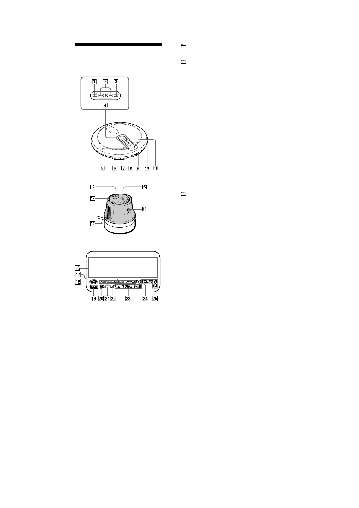
CD player
Display
SECTION 2
GENERAL
1
2
./> buttons
3
4
Jog lever
VOL (volume) +/−
U/u
u
5
CD player:
x
Rotary commander:
x
6
i (headphones) jack
7
DC IN 3 V jack
8
HOLD switch (on the back of the CD
player)
9
OPEN switch
q;
SEARCH button
qa
DISPLAY/MENU button
qs
u (play/pause) button
qd
./> control
qf
Jack for connecting a car connecting pack
qg
Push down and turn.
qh
Character information display
qj
Atrac3plus/MP3 indicator
qk
Disc indicator
ql
Battery indicator
w;
Play list indicator
wa
Group indicator
ws
Bookmark indicator
wd
Play mode indicator
wf
Timer indicator
wg
Sound indicator
* This button has a tactile dot.
This section is extracted from
instruction manual.
(group) − button
(group) + button
(play/pause)*
STOP button
(stop) button
(group) +/− control
4

• This set can be disassembled in the order shown below.
3-1. DISASSEMBLY FLOW
SET
3-2. CABINET LOWER SUB ASSY, UPPER LID SUB ASSY
(Page 5)
D-NE331CK/NE336CK
SECTION 3
DISASSEMBLY
3-3. MAIN BOARD, OPTICAL PICK-UP ASSY (CDM-3325ERV2)
(Page 6)
Note: Follow the disassembly procedure in the numerical order given.
3-2. CABINET LOWER SUB ASSY, UPPER LID SUB ASSY
2
two screws
3-4. SWITCH BOARD
(Page 6)
3
two claws
2
four screws
5
flexible flat cable (10 core)
(CN604)
6
upper lid sub assy
3
two claws
4
cabinet lower sub assy
1
Open the upper lid.
MAIN board
S802
Note: On installation of MAIN board,
adjust the position of switch (S802)
and hold knob.
hold knob
3
two claws
5
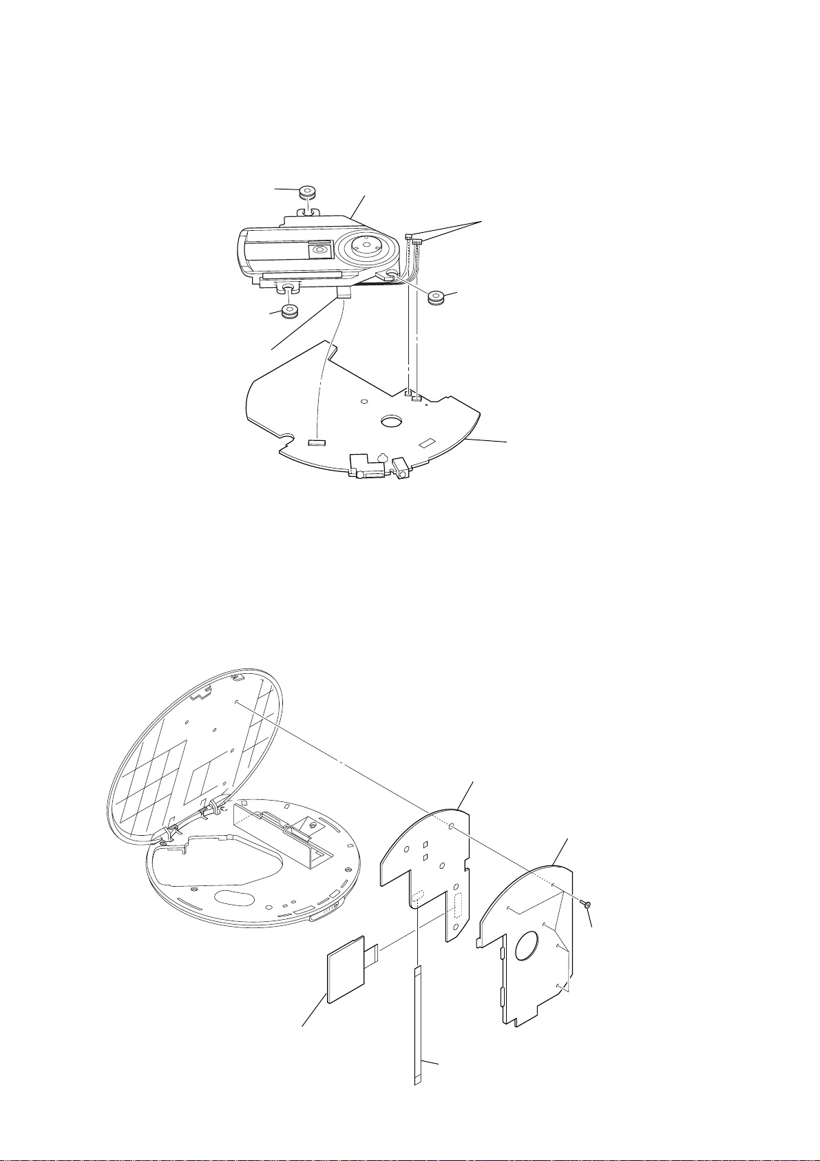
D-NE331CK/NE336CK
s
3-3. MAIN BOARD, OPTICAL PICK-UP ASSY (CDM-3325ERV2)
5
4
4
insulator
1
OP flexible board
(CN603)
insulator
optical pick-up assy
(CDM-3325ERV2)
4
insulator
2
two connectors
(CN601, CN602)
3-4. SWITCH BOARD
5
SWITCH board
3
MAIN board
2
lid cover
1
five screw
3
liquid crystal display panel
(LCD1001) (CN1001)
4
flexible flat cable (10 core)
(CN1002)
6

SECTION 4
DIAGRAMS
• Note for Printed Wiring Boards and Schematic Diagrams
D-NE331CK/NE336CK
Note on Printed Wiring Board:
• X : parts extracted from the component side.
• Y : parts extracted from the conductor side.
• z : Through hole.
• : Pattern from the side which enables seeing.
(The other layers' patterns are not indicated.)
Caution:
Pattern face side: Parts on the pattern face side seen from
(Conductor Side) the pattern face are indicated.
Parts face side: Parts on the parts face side seen from
(Component Side) the parts face are indicated.
Note on Schematic Diagram:
• All capacitors are in µF unless otherwise noted. (p: pF)
50 WV or less are not indicated except for electrolytics
and tantalums.
• All resistors are in Ω and 1/
specified.
• C : panel designation.
Note: The components identified by mark 0 or dotted line
with mark 0 are critical for safety.
Replace only with part number specified.
• A : B+ Line.
• Power voltage is dc 1.5 V and fed with regulated dc power
supply from battery teminal.
• Voltages and waveforms are dc with respect to ground
under no-signal conditions.
no mark : CD PLAY
• Voltages are taken with a VOM (Input impedance 10 MΩ).
Voltage variations may be noted due to normal production tolerances.
• Waveforms are taken with a oscilloscope.
Voltage variations may be noted due to normal production tolerances.
• Circled numbers refer to waveforms.
• Signal path.
J : CD PLAY
4
W or less unless otherwise
7
D-NE331CK/NE336CK
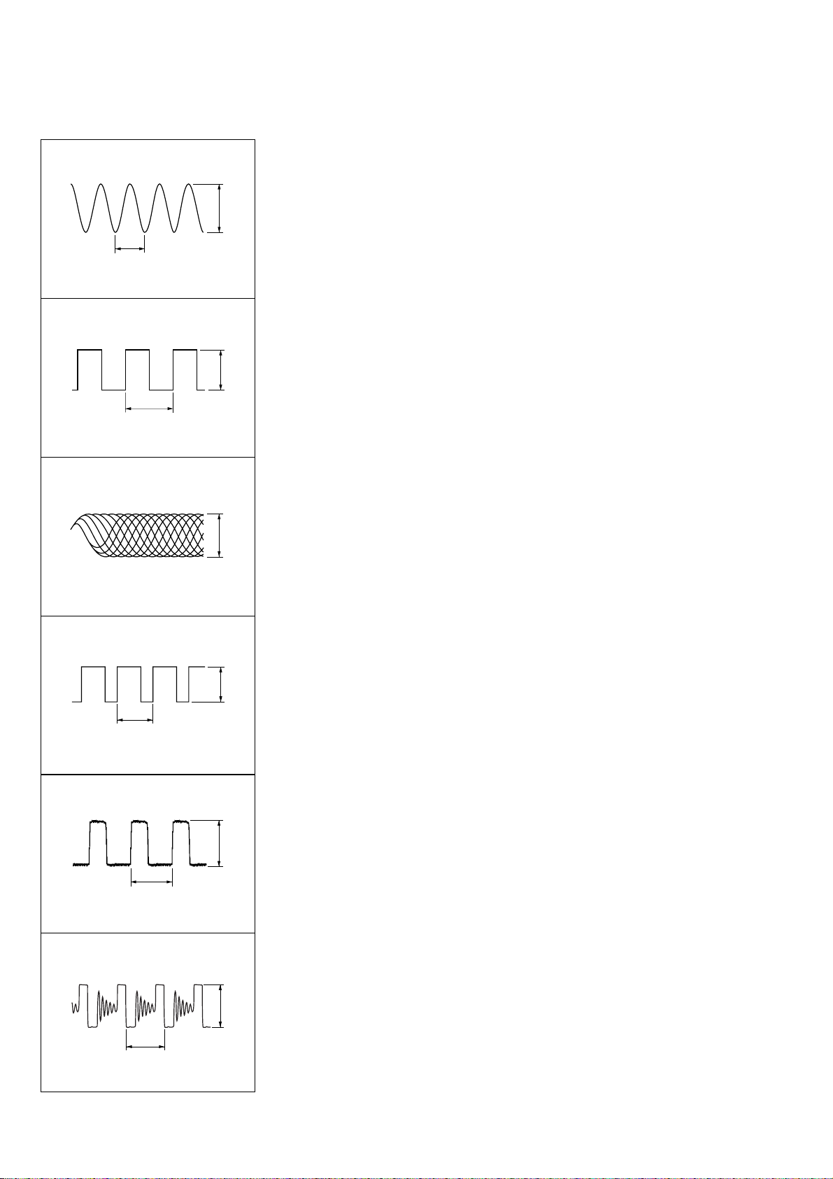
• Waveforms
– MAIN Board –
IC801 tg (XTAL)
1
1.1 Vp-p
45.5 ns
500 mV/DIV, 20 ns/DIV
IC801 yd (SYNC)
2
(CD play mode)
2.2 Vp-p
5.7 µs
1 V/DIV, 2 µs/DIV
IC801 if (RFACI)
3
(CD play mode)
200 mV/DIV, 200 ns/DIV
IC401 9 (L2L)
4
5.7 µs
1 V/DIV, 2 µs/DIV
IC302 5 (EXT), Q301 (Gate)
5
550 mVp-p
2.6 Vp-p
6
8
3.7 µs
2.2 Vp-p
1 V/DIV, 1 µs/DIV
Q301 (Drain)
3.6 Vp-p
3.7 µs
2 V/DIV, 1 µs/DIV
D-NE331CK/NE336CK
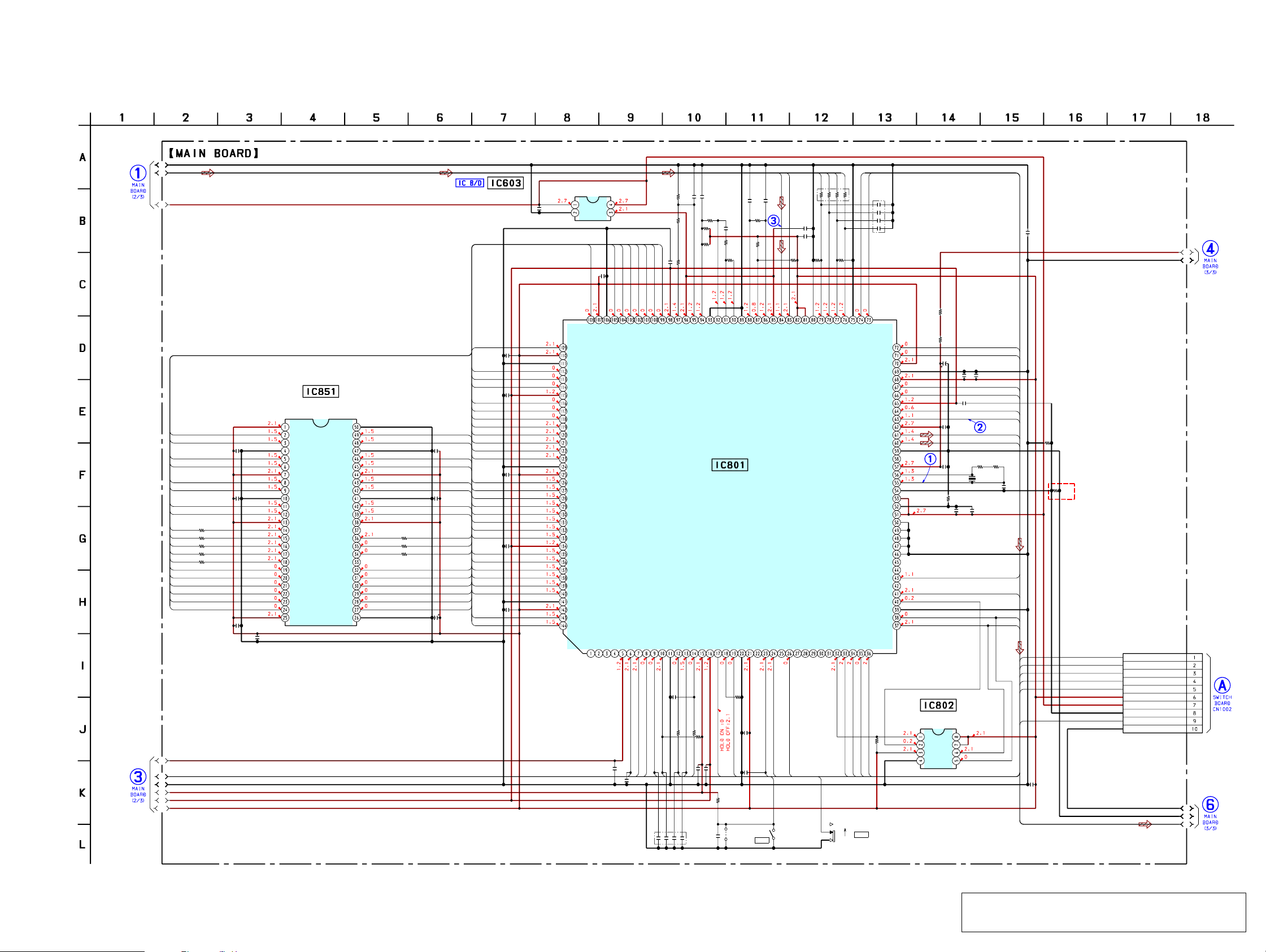
4-1. SCHEMATIC DIAGRAM – MAIN Board (1/3) –
(1/3)
VCC
DQ1
DQ2
VSSQ
DQ3
DQ4
VCCQ
DQ5
DQ6
VSSQ
DQ7
DQ8
VCCQ
LDQM
XWE
XCAS
XRAS
XCS
A11
A10
A0
A1
A2
A3
VCC
SD-RAM
IC851
MSM56X16160J
-20T3
UDQM
(Page 10)
(Page 10)
A1
A2
A3
SDDQ1
SDDQ2
SDDQ3
SDDQ4
SDDQ5
SDDQ6
SDDQ7
SDDQ8
SDLDQM
SDXWE
SDXCAS
SDXRAS
SDXCS
SDA11
SDA10
SDA0
SDA1
SDA2
SDA3
A5
A6
A7
A8
A9
A10
C895
C897
0
R859
0
R855
R856
22
R860
22
0
R858
C898 C899
0.1
0.1
0.1 0.1
• See page 8 for Waveforms. • See page 16 for IC Block Diagrams. • See page 16 for IC Pin Function Description.
B
F
A
RFDC
OPGUP
RFDC
HG_GUP
C611
1
C862
0.1
R617
22k
IGEN
AVDSAD
VOL_LATCH
CLOCK_SHIFT
E
22k
RB601
100k
R612
E
VC
DBG_MNT_I
DBG_MNT_O
HOLD
A
TSB
100k
R620
F
B
XSCK1
XEEPROM_CS
XSCKI
OFF
SFDR
SFDR
AVSSAD
S01
SI1
SI1
SO1
S802
HOLD
0.1
C602
R606
2.2k
R607
2.2k
FILI
FILO
IC801
CXR721260-203R
X_HOLD
OPEN
HOLD
R811
1M
0.47
RFACI
C610
C608
R614
220k
R616
0.1
47k
PCO
BIAS
ASYI
ASY0
RFACI
AVDASM
VDIO
OPEN
HG_STB_O
LCD_XRST_O
ECO
LCD_XRST
OPSTB
OPEN
OPEN(OPEN) HOLD
AMUTE
AMUTE_O
100k
R894
AVSASM
VSS
0.1
C837
0.1
C894
IC603
+2.1V REGULATOR
C603
1
SDUDQM
C829
0.1
SDA3
SDA2
SDA1
C828
0.1
SDA0
SDA10
SDA11
VSS
DQ16
DQ15
VSSQ
DQ14
DQ13
VCCQ
DQ12
DQ11
VSSQ
DQ10
DQ9
VCCQ
NC
CLK
CKE
NC
A9
A8
A7
A6
A5
A4
VSS
0
R865
R866
22
R867
22
SDXCS
SDDQ16
SDXRAS
SDDQ15
SDXCAS
C892
SDXWE
0.1
SDDQ14
SDLDQM
SDDQ13
SDDQ12
SDDQ11
C893
0.1
SDDQ10
SDDQ9
SDUDQM
SDCLK
SDCKE
SDA9
SDA8
SDA7
SDA6
SDA5
SDA4
C891
22
6.3V
SDDQ8
SDDQ7
SDDQ6
SDDQ5
SDDQ4
SDDQ3
SDDQ2
SDDQ1
SDDQ16
SDDQ15
SDDQ14
SDDQ13
SDDQ12
SDDQ11
SDDQ10
SDDQ09
C832
0.1
C838
0.1
C833
0.1
XC6213B212NR
CE
VIN
VSS
VOUT
C831
SDA5
SDA4
0.1
SDCKE
SDCLK
VSS
SDA4
SDCKE
SDCLK
VDIOSD
SDUDQM
VDIOSD
VSS
SDA3
SDA2
SDA1
DVDD
SDA0
SDA10
SDA11
SDNCS
SDNRAS
SDNCAS
SDNWE
SDLDQM
VSS
VDIOSD SYSTEM CONTROLLER,DSP,LCD DRIVER
SDDQ8
SDDQ7
SDDQ6
SDDQ5
SDDQ4
SDDQ3
SDDQ2
SDDQ1
DVDD
SDDQ16
SDDQ15
SDDQ14
SDDQ13
SDDQ12
SDDQ11
VSS
VDIOSD
SDDQ10
SDDQ9
DVDBK
XTRST
TDI
TMS
TCK
C834
XRST
0.1
C803
R604 C607
1M 0.47
R613
220k
0.1
C883
SDA9
SDA8
SDA6
SDA7
SDA9
SDA8
SDA7
SDA6
SDA5
XRST
XWAKE
XADEVENT
OPEN
0.1
CASINO_WAKE
DCINMNT
AD_KEY1
AD_DCINMNT
DVDD
AVSAD
KEY1
1
C806
22k
R615
VPCO
RMKEY
1k
R812
AD_RMKEY
AVDVCO
BATMNT
1k
R814
AD_BATMNT
AD_CHGMNT
C805
4700p
VCTL
CHGMNT
C601
4700p
R601
47k
10k
R611
R610
100k
CLTV
AVSVC0
DVDD
AVDAD
10k
R623
0.1
0.1
C835
C836
C810 SL805 S801
0.01
SRDR
SRDR
DAMPCLK
TESTMODE
POW.LATCH
LCD_CS
R820
100k
LCD_CS
CB605
470P
VDIOSD2
VDIODSP
VDIOAMP
VSSAMP
AVDMO
AVSMO
AVDPLL0
AVSPLL1
AVDPLL1
TU BEEP
PWML
PWMR
EXTAL
TEST 2
TEST 3
ATEST
XSCK0
0.1
C847
B2
B3
(Page 11)
R999
0
R851
TFDR
TRDR
VSS
FFDR
FRDR
DVDD
MDP
SYNC
XTAL
EVA
RTCK
TDO
FG
SI0
VSS
SO0
47
C851
47
6.3V
EEPROM
IC802
AK6510CL-L
XCS
DO
_WP
GND
_HOLD
VCC
SCK
DI
C846
0.1
C840
0.1
R806
0
C845 C844
0.1 0.1
C841C843
C842
0.10.1
R647
10k
22.496MHz
TFDR
TRDR
FFDR
FRDR
0.1
MDP
SYNC
PWML
PWMR
R819
2.2k
X601
C680
3p
FG
POWERLT
SO0
XSCK0
R854
0
R807
(NE331CK)
0
CN604
XSCKI
LCD_CS
SO1
SI1
LCD_XRST
AD_KEY1
C875
0.1
CLK_I
LCD_CS_I
DATA_O
DATA_I
LCD_XRST
VCC2 2.1V
VCC3 2.7V
D_GND
AD_KEY1
SGND
10P
(Page
15)
B5
B6
B7
(Page 11)
D-NE331CK/NE336CK
When MAIN board is replaced or EEPROM (IC802) on the MAIN board is
replaced, patch processing is needed.
99
Confirm about information of patch processing to each service headquarters.
D-NE331CK/NE336CK
4-2. SCHEMATIC DIAGRAM – MAIN Board (2/3) –
CN603
15P
OPGSW
A
B
RF
OPSTB
LD
PD
GND_A
VCC
E
F
F+
T-
T+
F-
CN601
M601
(SPINDLE)
U
W
DRY BATTERY
(IEC DESIGNATION LR6)
M602
(SLED)
SIZE"AA"
1PC. 1.5V
DC IN 3V
N
V
(Page 9)
J401
4P
COM
W
V
U
CN602
2P
S+
S-
A2
A3
A1
C404
0.1
C403
220
6.3V
F401
1.4A
TH401
32V
C402
L410
C401
L411
1
W401
W402
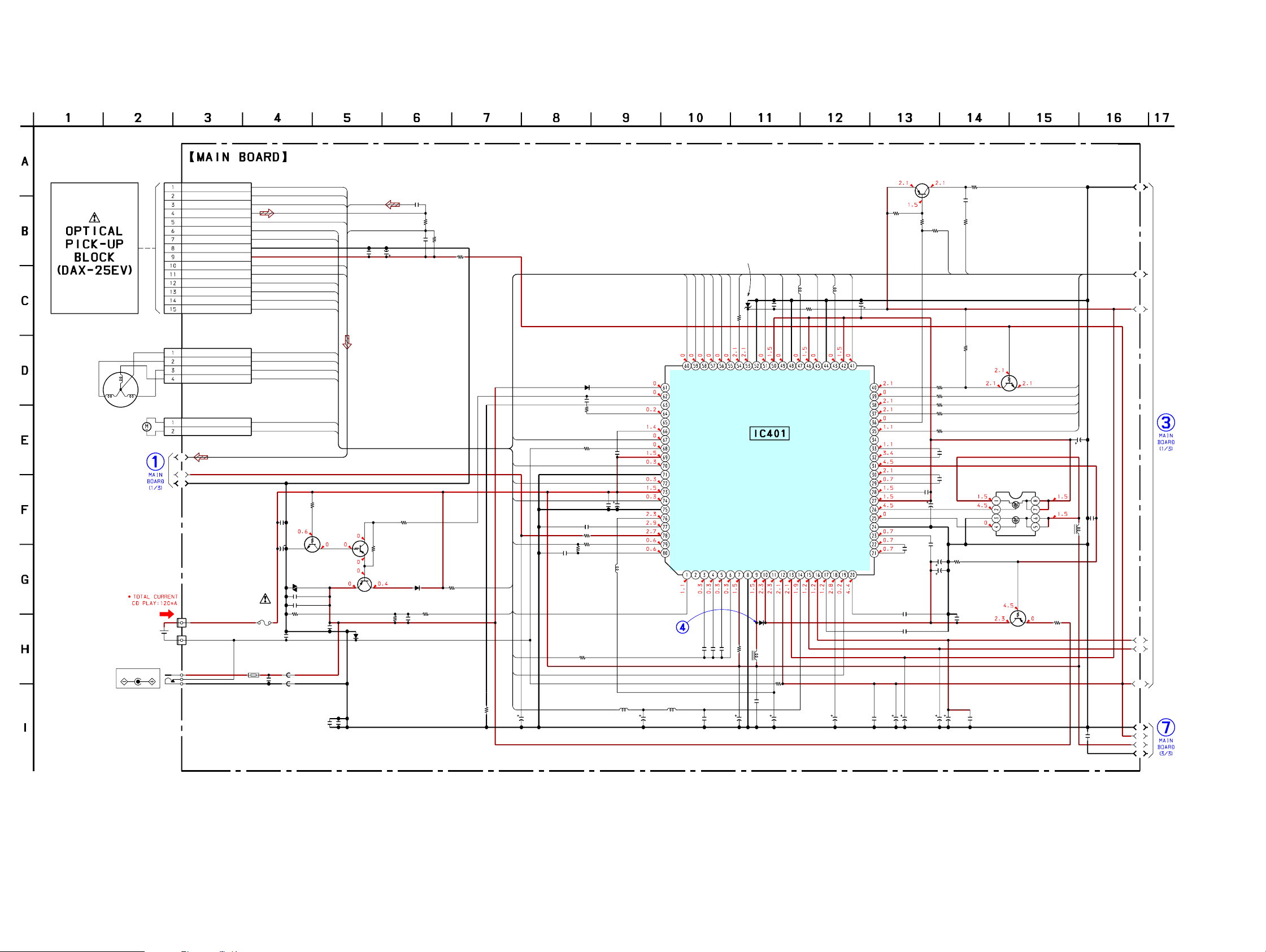
• See page 8 for Waveforms. • See page 16 for IC Pin Function Description.
(2/3)
OPGUP
DTC144TUA-T106
1
VDR401
C408
C411
R405
A
RFACI
B
OPSTB
RFDC
LD
PD
E
F
F+
T-
T+
F-
COM
W
V
U
S+
S-
R411
470k
Q408
DTA144TUA-T106
R401
Q402
2SA1363-T111-1E
MBR120LSFT1
4.7k
D402
Q406
10
10
10k
C410
1
C460
1000p
C461
1000p
C605
22
6.3V
Q401,402,404
RIPPLE FILTER
R404
47k
C609
2200p
C614C604
22p0.1
R406
100
D403
MA2YD2300LS0
C409 R410
0.22 47k
R609
22k
R619
47k
R631
10
D406
MA2SD3100LS0
C437
100p
R452
100k
AD_BATMNT
R470
47k
AD_DCINMNT
AD_CHGMNT
U
V
W
MDP
FG
COM
PD
R400
0
LD
C444
47
6.3V
R455
1k
C438
1000p
C452
0.1
C439
4.7
L408
0
0
R456
C445
R457
47k
4.7
L407
47µH
R416
47k
47µH47µH
R426
470k
Q407
2SA1832FV
(TH3SONY)
DC DETECT
R423 R417
R425
220k 10k
220k
D441
RSB6.8STE61
R
D
D
FF
FR
3
1
F
DCIN
RF1
RS1
INM1
CHGSW
INP1
CHGMNT
BATM
VD4
U
MGND4
V
VD5
47 6.3V
C443
W
MGND5
L3L
VLGO3
VCC3
PWM
APWM
G
F
L409L402
C448
47
6.3V
DR
D
TFD
TR
SFD
SR
1
2
2
3
1
1
1
1
F
F
R
R
K
R
I
I
I
B
U
V
W
X
1000p
1000p
1000p
C414
C415
C416
C822
C426
47
1
6.3V
S
S
R
X
0
R454
1
T
1
B
1
T
S
D
R
S
R
N
R
N
G
M
FOCUS/TRACKING COIL DRIVE,
SPINDLE/SLED MOTOR DRIVE,
POWER CONTROL
IC401
TB2169AFG(O)
2
D
N
M
L
G
IN
O
2
L
P
V
C
0
22µH
R437
L401
C821
0.1
+
T
R
R
R
R
C446
2200
1
1
D
O
F
V
W
0
S
C
W
C
P
V
D404
MA785-(TX).SO
S-
R482
22k
6.3V
+
T
R442
L406 L405
47µH47µH
2
2
1
D
1
D
O
O
D
F
V
R
N
G
M
1
2
2
C
B
B
C
T
P
T
C
S
A
S
V
V
V
V
47
T
F+
F-
C442
47
6.3V100k
3
3
3
2
O
R
1
C
C
V
3
2
D
O
O
F
D
V
R
N
LATCH
G
M
DATA
CLOCK
WAKE UP
RMCR
SYNC
COLD ST
C1L
C1H
VG
RF7
INM7
INP7
VD
UPCKB7
UPCK7
GND
INP2
RF2
2
Y
F
A
M
G
E
L
E
D
W
R
D
P
P
V
C423C418
C463
4.7
1
6.3V
C429
IN
0.01
C427
0.047
C419
100
6.3V
C433
4700p
C430
4700p
C450
47
6.3V
C449
6.3V
0.1
C428
C421
C420
47
22
6.3V
6.3V
C405
0.22
R422
10k
T
N
M
EY
K
IN
M
DC
_
_R
D
AD
A
R480
100k
0
R436
0
R435
0
R434
0
R433
0
R431
C436
0.22
C435
0.01
C432
47 6.3V
R465
220k
100
Q412
DTA143TE-TL
C451
SWITCHING
1
C422
C464
47
1
6.3V
NTHD4508N
B+ SWITCH
S
S
DTC115TE-TL
SWITCHING
Q405
Q411
POWERLT
SO0
XSCK0
XWAKE
SYNC
C431
47 6.3V
0.1
C434
L404
10µH
R464
220
C462
47p
A7
A6
A8
A9
A5
A10
C1
C2
C3
C4
(Page 9)
(Page 11)
D-NE331CK/NE336CK
1010
D-NE331CK/NE336CK
4-3. SCHEMATIC DIAGRAM – MAIN Board (3/3) –
(3/3)
R104
10k
C105
4.7
R105
6.3V
33k
R205
C205
C113C110
220p2200p
C213C211
220p4700p
6.3V
33k
4.7
R204
10k
PWMR
PWML
R112
470
R212
470
C210
2200p
220
R213
220
C111
4700p
R114R113
4.7k
R214
4.7k
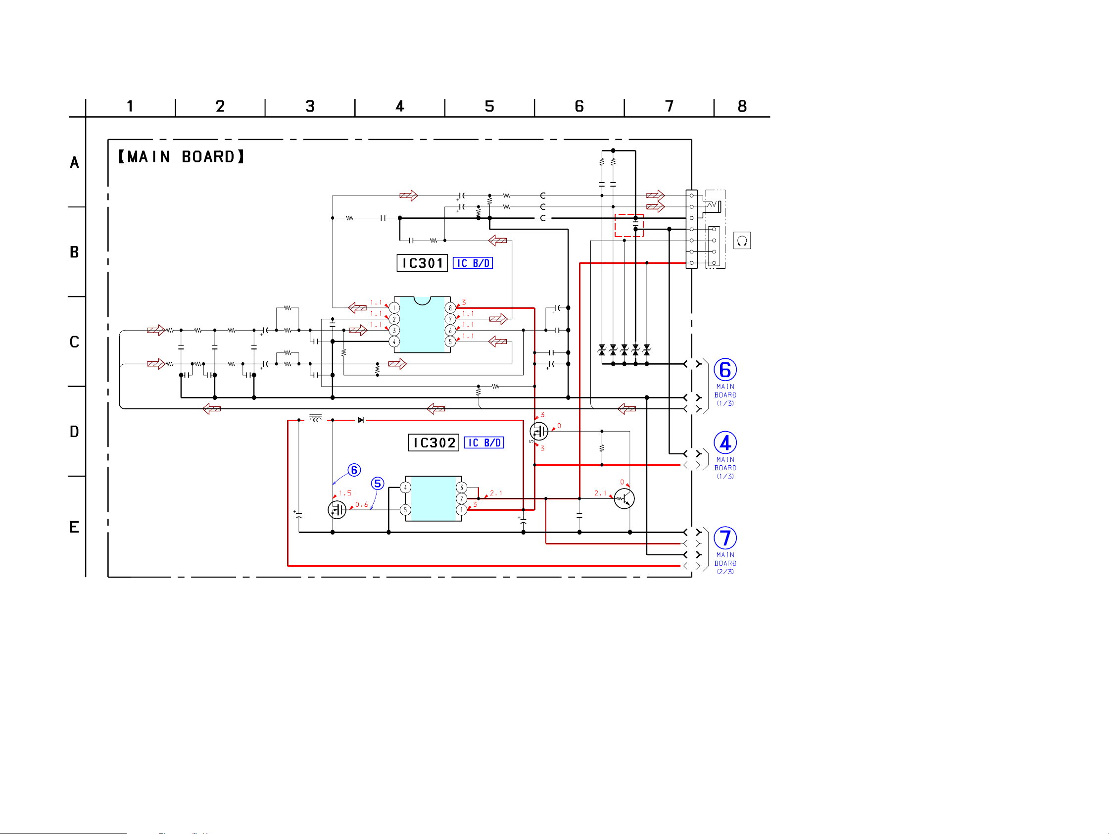
• See page 8 for Waveforms. • See page 16 for IC Block Diagrams.
C108
R109
C106
470p
C206
470p
C307
L302
22µH
47
4V
C305
1
S
R108 C107
10 1000p
D301
MA2Z748001S0
Q301
XP151A13A0MR
DC/DC CONVERTER
R206R106
10k10k
HEADPHONE AMP
IC301
BH35544F-FE2
OUT1
XMUTE
IN1
GND
DC/DC CONVERTER
XC6367A281MR
GND
EXT
R208C207
OUT2
BIAS
IC302
220
C208
220
101000p
VCC
IN2
CE
VDD
VOUT
1k
4V
R209
1k
4V
R307
AMUTE
R302
220k
C306
6.3V
R110
R210
680k
100
0
0
100 6.3V
FB101
FB201
FB301
C303
22
6.3V
C304
0.1
C302
0.1
C301
Q302
CPH3303-TL
C308
1
Q302,303
B+ SWITCH
R111
2.2
C109
0.22
AD_RMKEY
R308
1M
Q303
DTC115TUA
-T106
R211
C209
0.22
0.033
RSB6.8STE61
RSB6.8STE61
D201
D101
2.2
C309
RSB6.8STE61
RSB6.8STE61
D304
D302
(NE336CK)
RSB6.8STE61
D303
B5
B6
B7
B3
B2
C1
C2
C4
C3
J301
(Page 9)
(Page 9)
(Page 10)
D-NE331CK/NE336CK
1111
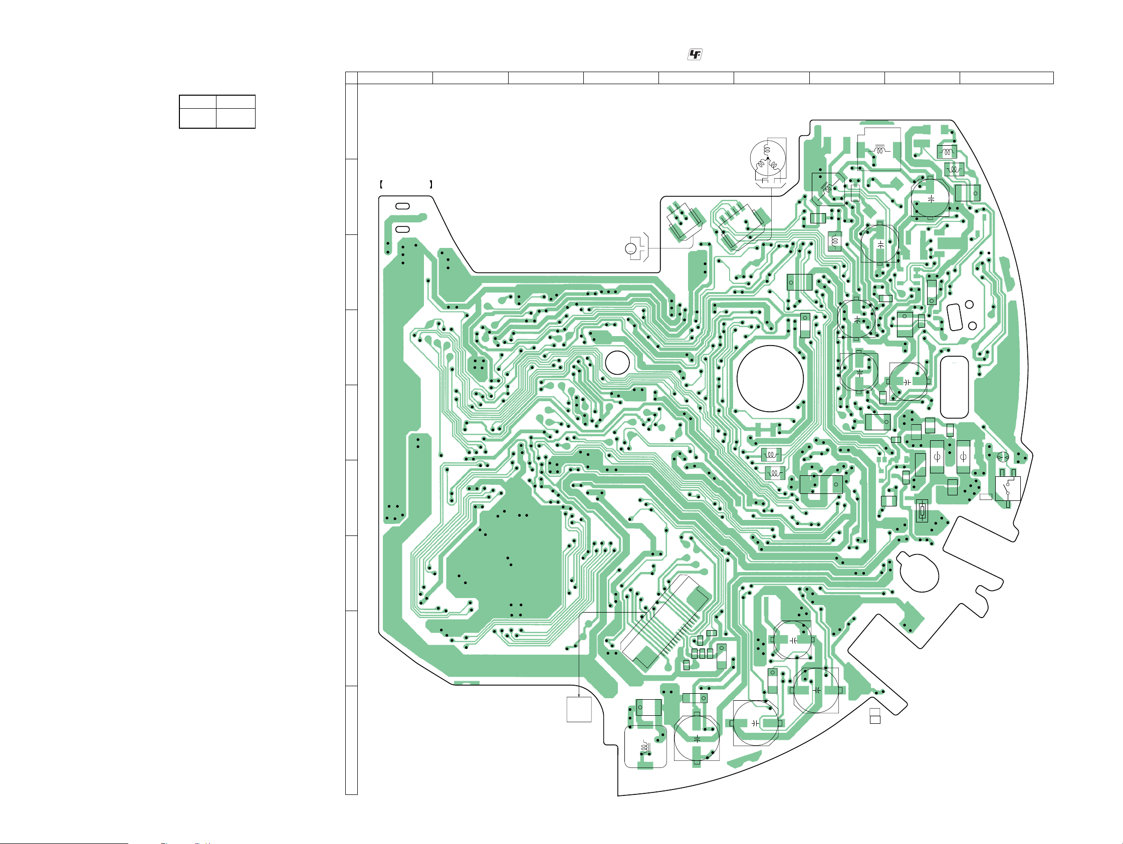
D-NE331CK/NE336CK
• Semiconductor
Location
Ref. No. Location
D402 F-8
D404 B-7
4-4. PRINTED WIRING BOARD – MAIN Board (Component Side) –
1 2 3 4 5 6 7 8 9
A
MAIN BOARD
(COMPONENT SIDE)
B
M602
M
(SLED)
C
: Uses unleaded solder.
C418
L401
AK
D404
C443
+
R437
+
+
C419
V
M601
(SPINDLE)
1
2
CN602
1
4
CN601
UW
4
1
+
L404
L408
L407
C442
+
C444
C463
C822
L402
L409
+
C420
+
C448
+
D
C422
+
E
L406
L405
+
C403
C449
F
C464
C411
C421
+
+
R400
C402
C410
D402
A
K
C408
L410 L411
TH401
VDR401
C401
S801
OPEN
SL805
(OPEN)
G
C604
C306
C108
C614
15
R609
+
+
R619
C609
R631
+
C605
C301
C303
+
+
C105
+
C208
+
11
(11)
1-868-466-
CN603
H
1
OPTICAL
PICK-UP
BLOCK
(DAX-25EV)
I
+
C307
L302
D-NE331CK/NE336CK
1212
 Loading...