

D-NE240/NE241/NE241CK
SERVICE MANUAL
Ver. 1.0 2006.10
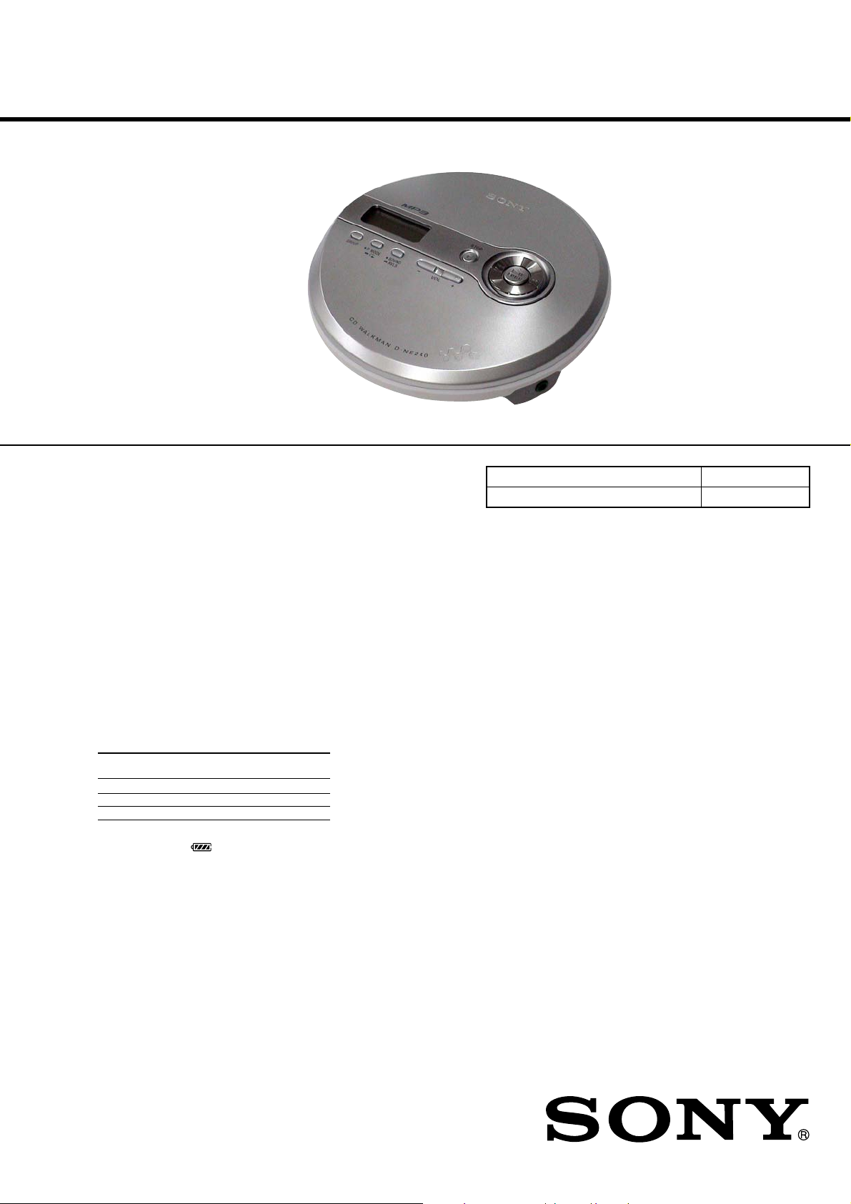
Photo: D-NE240
SPECIFICATIONS
AEP Model
D-NE240/NE241
E Model
D-NE241/NE241CK
Model Name Using Similar Mechanism D-NE005
CD Mechanism Type CDM-3525A
System
Compact disc digital audio system
Laser diode properties
Emission duration: Continuous
Laser output: Less than 44.6 µW (This output is the value measured
at a distance of 200 mm from the objective lens surface on the
optical pick-up block with 7 mm aperture.)
Power requirements
• Two LR6 (size AA) batteries: 1.5 V DC × 2
• AC power adaptor (DC IN 4.5 V jack):
100 - 240 V, 50/60 Hz
Battery life* (approx. hours)
(When the CD player is used on a flat and stable place.)
Playing time varies depending on how the CD player is used.
When using two Sony alkaline batteries LR6 (SG)
(produced in Japan)
G-PROTECTION G-on G-off
Audio CD 16 11
MP3 CD (Recorded at 128 kbps) 23 23
* Measured value by the standard of JEITA (Japan Electronics and
Information Technology Industries Association).
• The indicator sections of
battery power. One section does not always indicate one-fourth of
the battery power.
roughly show the remaining
Dimensions (w/h/d) (without projecting parts and controls)
Approx. 140.0 × 32.7 × 140.0 mm
Mass (excluding accessories)
Approx. 210 g
Operating temperature
5°C - 35°C
MPEG Layer-3 audio coding technology and patents
licensed from Fraunhofer IIS and Thomson.
Design and specifications are subject to change without notice.
Supplied accessories
AC power adaptor (1) (except NE240)
Headphones (1)
Connection Cord (1) (NE241CK)
Car battery cord (1) (NE241CK)
Magic tape (1) (NE241CK)
9-887-425-01
2006J05-1
© 2006.10
PORTABLE CD PLAYER
Sony Corporation
Personal Audio Division
Published by Sony Techno Create Corporation
D-NE240/NE241/NE241CK
TABLE OF CONTENTS
1. SERVICING NOTES ............................................... 3
2. GENERAL ................................................................... 4
3. DISASSEMBLY
3-1. Disassembly Flow ........................................................... 5
3-2. Cabinet (Lower) Assy...................................................... 5
3-3. MAIN Board, CD Mechanism (CDM-3525A) ............... 6
3-4. Cabinet (Inner) Assy, SWITCH Board............................ 6
4. TEST MODE.............................................................. 7
5. ELECTRICAL CHECK........................................... 7
6. DIAGRAMS
6-1. Printed Wiring Board – SWITCH Board – ..................... 9
6-2. Printed Wir ing Board
– MAIN Board (Component Side) – ............................... 10
6-3. Printed Wir ing Board
– MAIN Board (Conductor Side) – ................................. 11
6-4. Schematic Diagram – MAIN Section (1/2) –.................. 12
6-5. Schematic Diagram – MAIN Section (2/2) –.................. 13
7. EXPLODED VIEWS
7-1. Upper Lid and Cabinet (Inner) Section ........................... 17
7-2. Cabinet Lower Section .................................................... 18
Notes on chip component replacement
• Never reuse a disconnected chip component.
• Notice that the minus side of a tantalum capacitor may be
damaged by heat.
Flexible Circuit Board Repairing
• Keep the temperature of the soldering iron around 270 ˚C
during repairing.
• Do not touch the soldering iron on the same conductor of the
circuit board (within 3 times).
• Be careful not to apply force on the conductor when soldering
or unsoldering.
CAUTION
Use of controls or adjustments or performance of procedures
other than those specified herein may result in hazardous radiation
exposure.
8. ELECTRICAL PARTS LIST................................ 19
On the AC power adaptor
• Use only the AC power adaptor supplied.
If your player is not supplied with an AC
power adaptor, use an AC-E45HG AC power
adaptor*. Do not use any other AC power
adaptor. It may cause a malfunction.
* Not available in Australia and some other
regions. Ask your dealer for detailed
information.
• Do not touch the AC power adaptor with wet hands.
• Connect the AC power adaptor to an easily accessible AC outlet.
Should you notice an abnormality in the AC power adaptor,
disconnect it from the AC outlet immediately.
Polarity of the
plug
SAFETY-RELATED COMPONENT WARNING!!
COMPONENTS IDENTIFIED BY MARK 0 OR DOTTED LINE
WITH MARK 0 ON THE SCHEMATIC DIAGRAMS AND IN
THE PARTS LIST ARE CRITICAL TO SAFE OPERATION.
REPLACE THESE COMPONENTS WITH SONY PARTS WHOSE
PART NUMBERS APPEAR AS SHOWN IN THIS MANUAL OR
IN SUPPLEMENTS PUBLISHED BY SONY.
2
SECTION 1
SERVICING NOTES
D-NE240/NE241/NE241CK
NOTES ON HANDLING THE OPTICAL PICK-UP
BLOCK OR BASE UNIT
The laser diode in the optical pick-up block may suffer electrostatic
breakdown because of the potential difference generated by the
charged electrostatic load, etc. on clothing and the human body.
During repair, pay attention to electrostatic breakdown and also use
the procedure in the printed matter which is included in the repair
parts.
The flexible board is easily damaged and should be handled with
care.
NOTES ON LASER DIODE EMISSION CHECK
The laser beam on this model is concentrated so as to be focused
on the disc reflective surface by the objective lens in the optical
pick-up block. Therefore, when checking the laser diode emission, observe from more than 30 cm away from the objecti ve lens.
OPERATION CHECK WHEN THE LID IS OPEN
In performing the repair with the power supplied to the set, removing
the MAIN board causes the set to be disabled.
In such a case, make a solder bridge to short SL801 (OPEN/CLOSE)
on the MAIN board in advance.
– MAIN Board (Component Side) –
LASER DIODE AND FOCUS SEARCH OPERATION
CHECK
During normal operation of the equipment, emission of the laser
diode is prohibited unless the upper lid is closed while turning ON
the S811. (push switch type)
The following checking method for the laser diode is operable.
• Method:
Emission of the laser diode is visually checked.
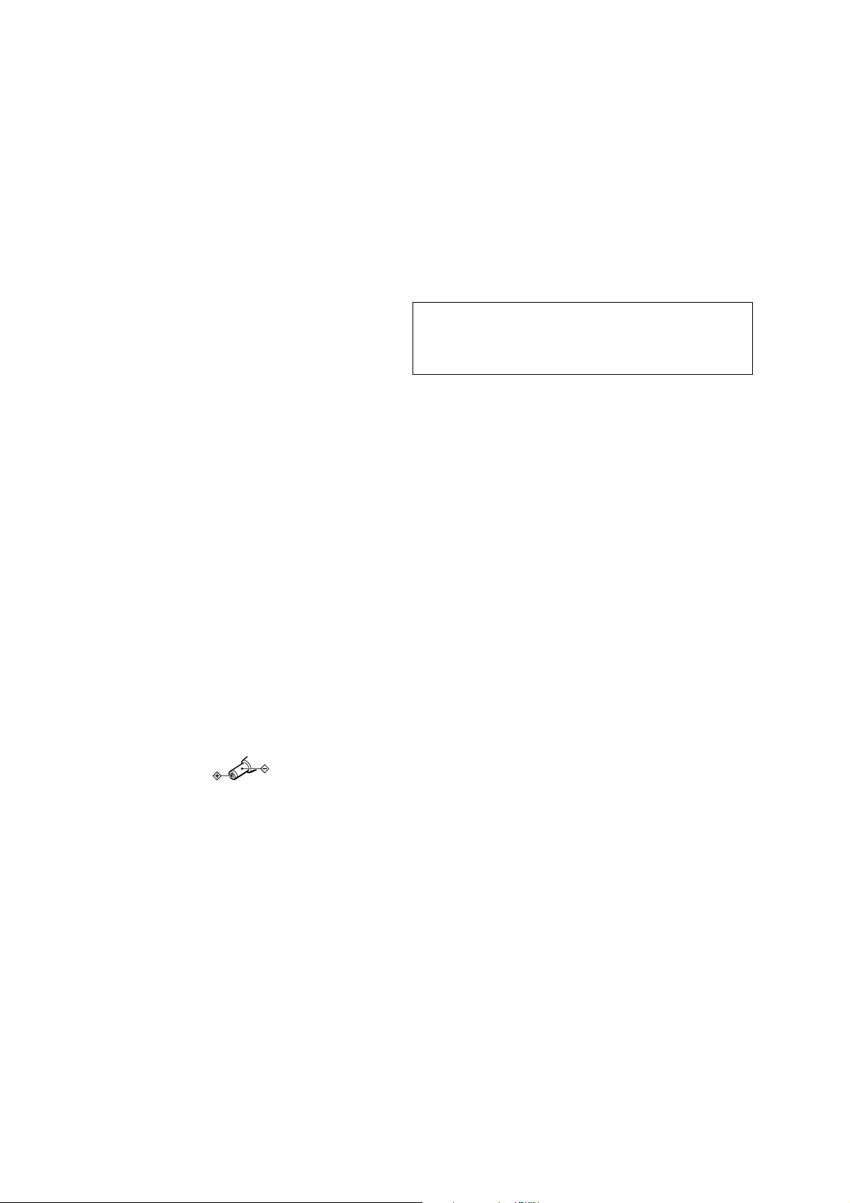
1. Open the upper lid.
2. With a disc not set, turn on the S811 with a screwdriv er having
a thin tip as shown in Fig.1.
3. Push the u button.
4. Observing the objective lens, check that the laser diode emits
light.
When the laser diode does not emit light, automatic power
control circuit or optical pickup is faulty.
In this operation, the objective lens will move up and down 4
times along with inward motion for the focus search.
S811
SL801
(OPEN/CLOSE)
COLOR VARIATION
Model Destination
D-NE240 AEP zz
AEP zz
D-NE241 E92 z
MX z
D-NE241CK MX z
• Abbreviation
E92 : 120V AC area in E model
MX : Mexican model
COLOR
BLACK SILVER
S811
MAIN board
Fig. 1 Method to push the S811
3
D-NE240/NE241/NE241CK
SECTION 2
GENERAL
This section is extracted from
instruction manual.
*(play/pause)
(lecture/pause)•ENTER
/ •
(group) (groupe) –/+
GROUP
P MODE/
SOUND/AVLS
VOL +*/–
(stop) (arrêt)•STOP
Display / Fenêtre d’affichage
Track number
Numéro de plage
Bookmark
Signet
Sound mode
Mode audio
Group indicator
Témoin du groupe
* The button has a tactile dot. / Ce bouton possède un point tactile.
DC IN 4.5 V
to an AC outlet
vers une prise secteur
AC power adaptor
Adaptateur secteur
OPEN
(headphones) jack
(casque d’écoute)
Prise
Headphones
Casque
HOLD (rear) (arrière)
Playing time
Temps de lecture
Play mode
Mode de lecture
Remaining battery power
Autonomie des piles
MP3 indicator
Témoin MP3
4
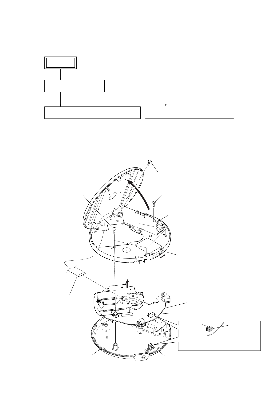
• This set can be disassembled in the order shown below.
3-1. DISASSEMBLY FLOW
SET
3-2. CABINET (LOWER) ASSY
(Page 5)
D-NE240/NE241/NE241CK
SECTION 3
DISASSEMBLY
3-3. MAIN BOARD, CD MECHANISM (CDM-3525A)
(Page 6)
Note: Follow the disassembly procedure in the numerical order given.
3-2. CABINET (LOWER) ASSY
3
four screws
3-4. CABINET (INNER) ASSY, SWITCH BOARD
(Page 6)
2
two screws
5
screw
4
Open the battery case lid.
7
flexible flat cable
(CN801)
9
cabinet (lower) assy
6
Lift up the CD mechanism.
knob (hold)
1
Open the upper lid.
8
MAIN board block
S812
knob (hold)
Note: On installation of MAIN board,
adjust the position of slide switch (S812)
and knob (hold).
S812
5
D-NE240/NE241/NE241CK
3-3. MAIN BOARD, CD MECHANISM (CDM-3525A)
3
insulator
orange
3
insulator
4
CD mechanism
(CDM-3525A)
2
flexible board
(CN501)
3
insulator
5
MAIN board
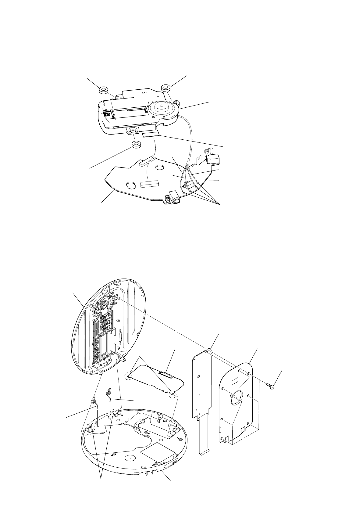
3-4. CABINET (INNER) ASSY, SWITCH BOARD
0
upper lid
4
two bosses
red
5
battery case lid
gray
black
9
SWITCH board
1
Remove four solders.
8
cover (upper lid)
7
eight screws
3
spring (R)
2
spring (L)
1
two bosses
6
cabinet (inner) assy
6

SECTION 4
p
TEST MODE
D-NE240/NE241/NE241CK
SECTION 5
ELECTRICAL ADJUSTMENTS
In the test mode, this set can check the microcomputer version and
liquid crystal display.
1) Short SL803 (TEST) on the MAIN board with a solder bridge.
Then, turn on the power.
2) Microcomputer version is displayed on the liquid crystal
display, and the liquid crystal display is all lighted.
3) Tuen off the power and open the solder bridge on SL803
(TEST) on the MAIN board.
Note: Remove the solders completely. Remaining could be shorted with
the chassis, etc.
– MAIN Board (Conductor Side) –
The CD section adjustments are done automatically in this set. In
case of operation check, confirm that focus bias.
Precautions for Cheack
1. Perform check in the order given.
2. Use YEDS-18 disc (P art No.: 3-702-101-01) unless otherwise
indicated.
3. Power supply voltage requirement: DC4.5 C in DC IN jack.
(J401)
HOLD switch: OFF
Connecting and Checking Location:
– MAIN Board (Conductor Side) –
TP604 (RF)
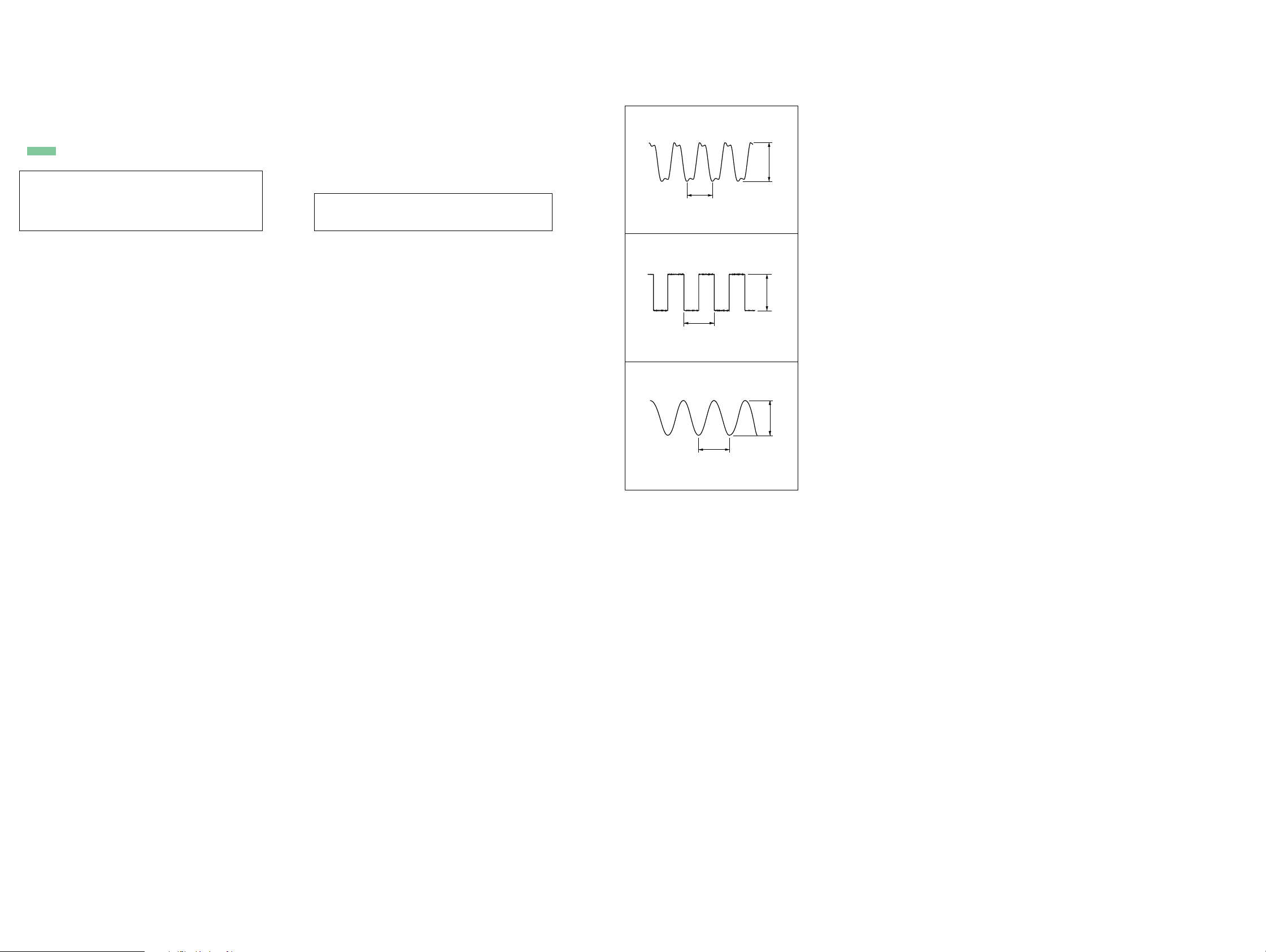
Focus Bias Check
Condition:
• Hold the set in horizonal state.
Connection:
oscilloscope
(AC range)
MAIN board TP604 (RF)
Procedure:
1. Connect the oscilloscope to the test point TP604 (RF) on the
MAIN board.
2. Set a disc. (YEDS-18)
3. Push the
4. Check the oscilloscope waveform is as shown below.
A good eye pattern means that the diamond shape (◊) in the
center of the waveform can be clearly distinguished.
u button.
+
–
RF Signal reference Waveform (Eye Pattern)
VOLT/DIV: 500 mV (With the 10:1 probe in use)
TIME/DIV: 500 ns
SL803
(TEST)
RF level
1.1 to 1.5 Vp-
To watch the eye pattem, set the oscilloscope to AC range and
increase the vertical sensitivity of the oscilloscope for easy
watching.
5. Stop revolving of the disc motor by pressing the x button.
D-NE240/NE241/NE241CK
77
D-NE240/NE241/NE241CK
SECTION 6
DIAGRAMS
• Note for Printed Wiring Boards and Schematic Diagrams
Note on Printed Wiring Board:
• X : parts extracted from the component side.
• Y : parts extracted from the conductor side.
• f : internal component.
• : Pattern from the side which enables seeing.
(The other layers' patterns are not indicated.)
Caution:
Pattern face side: Parts on the pattern face side seen from
(Conductor Side) the pattern face are indicated.
Parts face side: Parts on the parts face side seen from
(Component Side) the parts face are indicated.
Note on Schematic Diagram:
• All capacitors are in µF unless otherwise noted. (p: pF)
50 WV or less are not indicated except for electrolytics
and tantalums.
• All resistors are in Ω and 1/
specified.
• f : internal component.
• C : panel designation.
Note: The components identified by mark 0 or dotted line
with mark 0 are critical for safety.
Replace only with part number specified.
• A : B+ Line.
• Power voltage is dc 3 V and fed with regulated dc power
supply from battery terminal.
• Voltages and wavef orms are dc with respect to ground in
no-signal conditions.
no mark : CD PLAY
• Voltages are taken with a V OM (Input impedance 10 MΩ).
Voltage variations may be noted due to normal production tolerances.
• Waveforms are taken with a oscilloscope.
Voltage variations may be noted due to normal production tolerances.
• Circled numbers refer to waveforms.
• Signal path.
J : CD PLAY
4
W or less unless otherwise
• Waveforms
– MAIN Board –
IC601 tg (CLK)
1
237 ns
1 V/DIV, 100 ns/DIV
IC601 th (CLK88)
2
11.3 µs
1 V/DIV, 5 µs/DIV
IC601 ya (XO)
3
2.2 Vp-p
3.1 Vp-p
1.6Vp-p
59.4 ns
500 mV/DIV, 20 ns/DIV
D-NE240/NE241/NE241CK
88

D-NE240/NE241/NE241CK
6-1. PRINTED WIRING BOARD – SWITCH Board –
1 2 3 4 5 6 7 8 9
A
SWITCH BOARD
B
S801
u
ENTER
C
>
+
: Uses unleaded solder.
R849
S803S802
.
S801 – S809
S804
VOL +
R852
C819
30
R850 C820
S807
STOP
–
x
S805 S808 S809 S806
VOL – GROUP
CN802
SOUND
AVLS
P-MODE
F
R851
R853
R854
124
D
1
11
(11)
A
MAIN BOARD
CN801
(Page 10)
LCD801
LIQUID CRYSTAL DISPLAY
1-871-511-
D-NE240/NE241/NE241CK
99
D-NE240/NE241/NE241CK
CD MECHANISM BLOCK
CDM-3525A (1/2)
C632
C633
C620
C631
C618
C629
R626
RB602
RB601
R615
C615
C604
C609
FB602
CN801
R617
R613
R606
C611 C606
R614
R621
RB304
C105
R103
R203
C108
C301
RB301
C206
C106
VDR101
R202
R102
VDR201
C208
C303
R305
R304
RB305
C205
C324
RB331
RB330
C624
C101 C201
RB303
RB620
C625
R624
C619
C642
C634
IC603
FB605
R811
R618
R622
C637
IC601
Q602
Q321
Q323
Q320
R804
RB803
C871
C805
VDR801
CB414
R416
R417
R418
R407
R406
C413
R405
R401
R404
C405
C407
C406
L407
L406
CN403
CN408
CN407
CN404
SL801
C401
C421
L405
L404
F402
R402
R419
FB401
FB801
Q401
D403
IC401
IC802
1-871-510-
(11)
11
IC301
MAIN BOARD
(COMPONENT SIDE)
E
C
B
E
C
B
E
C
B
SWITCH BOARD
CN802
A
1
3
5
4
1C
2B
2C
1B
1E
2E
2C
1B
1C
2B
2E
1E
1
30
(OPEN/CLOSE)
A
B
C
D
E
F
G
H
1 2 3 4 5 6 7 8
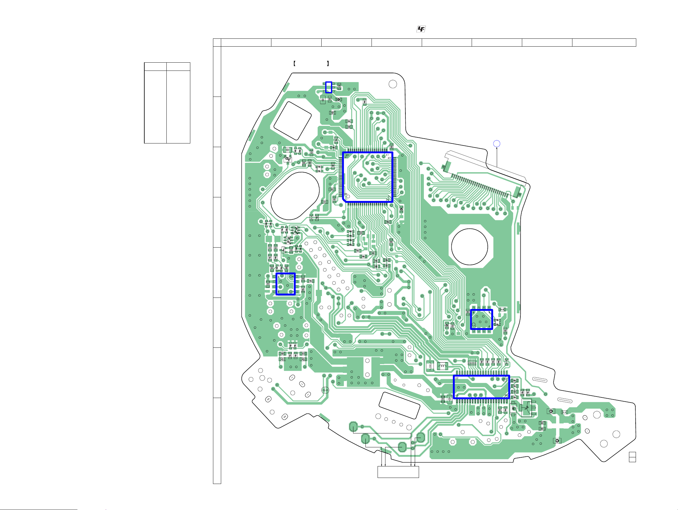
6-2. PRINTED WIRING BOARD – MAIN Board (Component Side) –
: Uses unleaded solder.
• Semiconductor
Location
Ref. No. Location
D403 H-6
IC301 E-2
IC401 G-6
IC601 C-3
IC603 A-3
IC802 F-6
Q320 E-2
Q321 D-2
Q323 D-2
Q401 H-7
Q602 C-2
(Page 9)
D-NE240/NE241/NE241CK
1010

D-NE240/NE241/NE241CK
6-3. PRINTED WIRING BOARD – MAIN Board (Conductor Side) –
1 2 3 4 5 6 7 8 9
A
B
C
R856
D
RB815
E
F
DRY BATTERY
SAZE "AA"
(IEC DESIGNATION LR6)
2PCS. 3V
G
CN401
CN402
D402
D406
H
VDR418
D404
R810
R422
C428
F401
C408
R828
R403
C409
R812
D803
C807
C411
Q402
1C
1B
D401
1E
2B
2E
2C
C404
L401
IC801
C410
C412
: Uses unleaded solder.
RB810
RB811
RB812RB813RB814
C806
R817
R818
SL803
(TEST)
R848
R847
C808
C802
R821
R827
Q403
R829
C416
C818
C431
C
VDR802
E
B
ECB
Q404
C419
+
R415
R414
C417
R823
C811
C403
L402
C812
C810
C814
RB801
C626
C623
C813
RB806
C809
+
L403
ON T OFF
MAIN BOARD
IC602
+
R835
+
C420
S812
HOLD
(CONDUCTOR SIDE)
R604
R410
+
C402
1
C601
TP604 (RF)
2
R603
C627
C612
+
C610
CN501
C640
R619
C602
Q601
B
CE
X601
15
C605
+
R201
R602
C210
Q324
1C
1E
2E
1B
2B
2C
16
R329
R323
C607
+
C603
C304
C204
+
R211 R111
FB301
L201
C628
R326
R327
C202
R321 R320
+
C321
1E
2E
2B
C104
L101
C630
C323
C320
Q322
+
C305
S811
• Semiconductor
Location
Ref. No. Location
D401 H-4
D402 H-3
D404 H-2
D406 H-2
D803 G-4
IC602 C-6
IC801 F-4
Q322 E-8
Q324 D-8
Q402 H-4
Q403 H-5
Q404 H-5
Q601 F-7
R328
C322
C102
R322
1C
1B
2C
+
R101
C110
1-871-510-
OPEN/CLOSE
J301
(11)
S811
DETECT
i
11
CD
MECHANISM
BLOCK
CDM-3525A
(2/2)
J401
DC IN 4.5V
+
–
D-NE240/NE241/NE241CK
1111
D-NE240/NE241/NE241CK
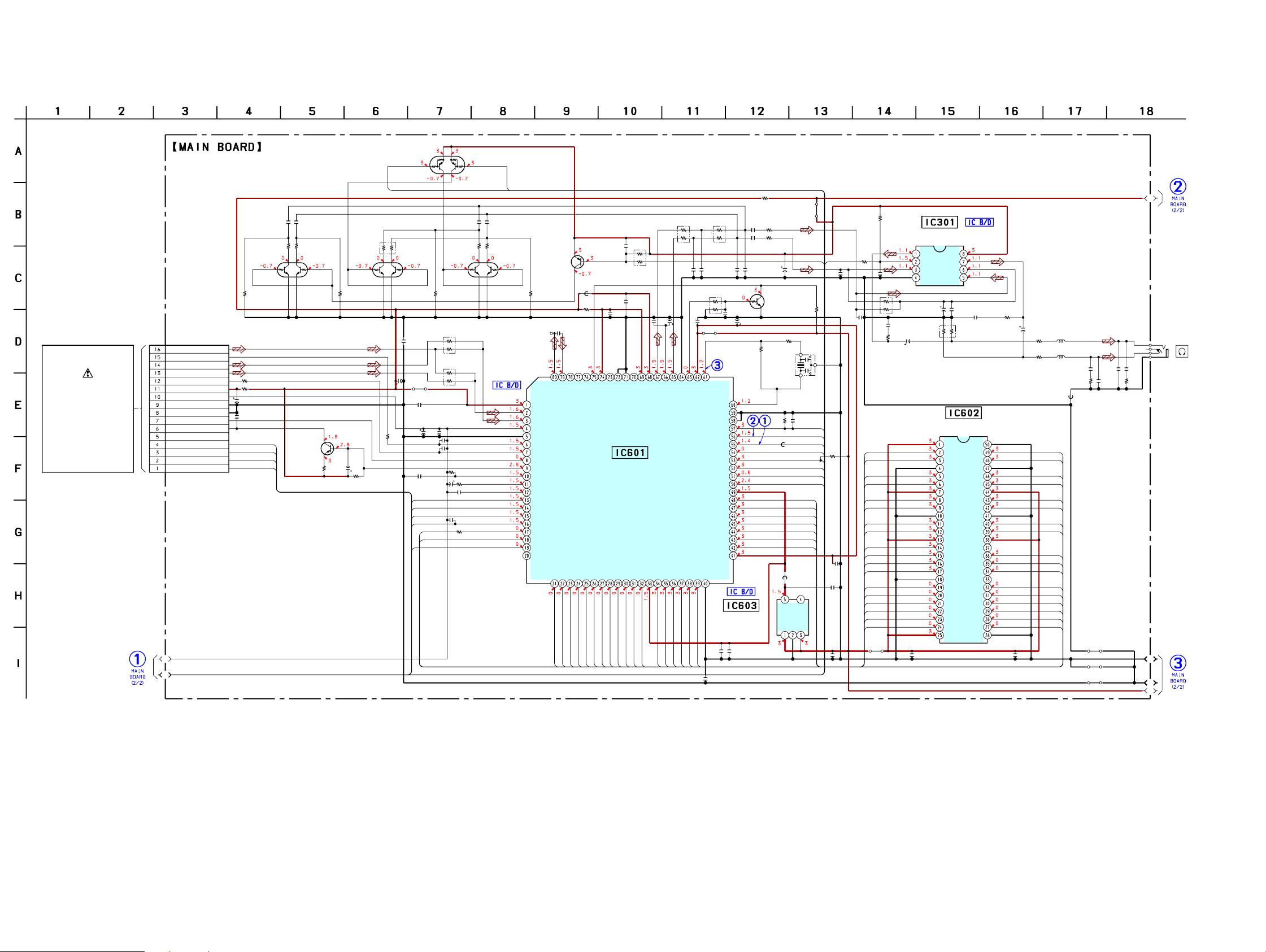
6-4. SCHEMATIC DIAGRAM – MAIN Board (1/2) –
(1/2)
C320 C321 C322 C323
0.047 0.047 0.047 0.047
R322
1M
CN501
16P
C
E
A
CD
MECHANISM
BLOCK
CDM-3525A
(1/2)
(Page 13)
B
F
VCC
VC
GND
GND
PD
LD
NC
F+
T+
T-
F-
A1
A2
68k
R613
2.2
R602
47 6.3V
C602
C603
0.01
F+
T+
T-
F-
• See page 8 for Waveforms. • See page 14 for IC Block Diagrams.
Q321
UMB2N-TN
FILTER SWITCH
-1-2
LPF_SW1
RB331R320 R321
LOW-PASS
FILTER
-1-2 -1-2 -1-2
Q601
2SA1602TP-1EF
AUTOMATIC
POWER
CONTROL
C601
R603
4.7
6.3V
1k220 220
R323
1M
47
R604
100k
LOW-PASS
RB601
Z623
C612
0.1
C607
C605
0.1476.3V
2200p
2200p
C606 R606
0.1 220k
4.7
50V 0.22
FDOUT
TDOUT
SDOUT
CLVOUT
CLK
CKE
A13
RB602
10k
10k
R614C610
C611
C604
0.1
R617
C402
0.01
C623
470
6.3V
R615
68k
C615
C609
470
100
UMH8NUMH8NUMH8N
LOW-PASS
FILTERFILTER
LPF_SW3
Q324Q323Q322
Q320
2SA2018TL
FILTER
SWITCH
R329R328
1M1M
C618
470p
TP604
(RF)
RFI
EQO
AVDD1
AC
BD
VBIAS
AGND1
E
F
PD
LD
ASY
PCO
FCO
FDOUT
TDOUT
SDOUT
CLVOUT
RCLK
RCKE
A13
A12
ANA_MONI1
ANA_MONI0
A08
A09
A10
A11
A08
A09
A10
A11
C324R327R326
0.472.2k2.2k
R621
R626 C629
C631
0.1
220 2.2
VSS_LD
VSS_RD
VDD_RD
HPRDACO
AD_MONI1
AD_MONI0
RF AMP,SERVO,DIGITAL SIGNAL PROCESSOR,
,SD-RAM CONTROLLER,D/A CONVERTER
IC601
BU9541JKV
A02
A03
A04
A05
A06
A07
A02
A03
A04
A05
A06
A07
RB330
A01
47k
HPLDAC0
A01
A00
VDD_LD
A00
AVDD2
VDD_CORE1
0.1
C628
10
16V
C620
VCDAC
LDACO
RDACO
WEX
CASX
RASX
WE
CAS
RAS
RB303 RB304
470 470
C101 C201 C102
2200p 2200p 1000p
RB620
10k
0.1 10 16V
C624 C630
Z601
XO
FLAG0
DVDD2
AGND2
DGND2
TESET
RESTB
CLK88
CLK
SUBSYQ
BUSY
MCK
DIN/DOUT
R/W
VDD_CORE2
DQ00
DQ01
DQ02
DQ03
DQ04
DQ05
DQ06
DVDD1
DGND1
DQ07
UDQM
LDQM
C633 C642
0.1 1
DQ07
UDQM
LDQM
C626
0.01
R410
1
C105
R103
2.2
22k
C205
R203
2.2
22k
C304
C202
100
1000p
6.3V
Q602
RT1N140M-TP-1
C625 R619
2.2 100k
XI
+1.5V REGULATOR
IC603
BH15FB1WG-TR
BUFFER
R618 R622
1M 220
X601
16.9344MHz
R624
100k
C619
0.1
FB602
FB605
VOUT
VSS
VIN
Z405
LPF_SW2 XHP_MUTE
RESTB
CLK88
CLK
R811
SUBSYQ
100k
BUSY
MCK
DIN/DOUT
R/W
DQ00
DQ01
DQ02
DQ03
DQ04
DQ05
DQ06
C637
0.1
C632
10
NC
CE
C634
1
A3
R304
1M
HEADPHONE AMP
IC301
R305
220k
C208
470p
C303
1
C108
470p
C210
1000p
R201
10
DQ00
DQ01
DQ02
DQ03
DQ04
DQ05
DQ06
DQ07
LDQM
WE
CAS
RAS
A11
A10
A00
A01
A02
A03
Z632
BH3544
OUT1
VCC
XMUTE
OUT2
IN1
BIAS
GND
IN2
C305
RB301
47
6.3V
C301
0.1
SD-RAM
IC602
M12L16161A-7T(J)
VCC
DQ0
DQ1
VSSQ
DQ2
DQ3
VCCQ
DQ4
DQ5
VSSQ
DQ6
DQ7
VCCQ
LDQM
XWE
CAS
RAS
XCS
A11
A10
A0
A1
A2
A3
VCC
R101
C110
1000p
VSS
DQ15
DQ14
VSSQ
DQ13
DQ12
VCCQ
DQ11
DQ10
VSSQ
DQ9
DQ8
VCCQ
NC
UDQM
CLK
CKE
NC
A9
A8
A7
A6
A5
A4
VSS
RB305
22k
C204
220
6.3V101k
C627 C640
4.7 4.7
C104
220
R211
6.3V
10
L201
R111 L101
10
UDQM
C106
VDR201
0.22
2200p
R102
VDR101
2.2
2200p
FB301
DQ00
DQ01
DQ02
DQ03
DQ04
DQ05
DQ06
DQ07
CLK
CKE
A09
A08
A07
A06
A05
A04
Z407
Z403
Z402
(Page 13)
J301
C206
0.22
R202
2.2
A6
A7
A8
(Page 13)
D-NE240/NE241/NE241CK
1212

D-NE240/NE241/NE241CK
6-5. SCHEMATIC DIAGRAM – MAIN Board (2/2) –
(2/2)
(Page 12)
A2
A1
CD
MECHANISM
BLOCK
CDM-3525A
(2/2)
DRY BATTERY
SIZE"AA"
(IEC DESIGNATION LR6)
2PCS. 3V
J401
DC IN 4.5V
CN404
CN403
CN407
CN408
Q401
2SB1132-T100-Q
+B SWITCH
F401
CN401
1P
CN402
1P
2A
32V
D406
UDZS-TE17-12B
D404
UDZS-TE17-12B
MA2YD2300LS0
F402
2A
32V
D403
VDR418
R403
1k
L404
L405
C421
0.22
MA2YD2300LS0
Q402
UMH8N
DC IN
DETECT
-1
-2
C401 R402
1 22k
D402
MAZ8062-TX
• See page 14 for IC Block Diagrams. • See page 15 for IC Pin Function Description.
Z401
C407
10
C406
0.1
C404
10
16V
C403
0.1
D401
C405
1000p
R404
100
L402
165µH
R401
100k
L401 330µ H
C409
R405
12k
C412
C410
C411
10 16V
R407
27k
2SD2652T106
1
0.1
470p
C413R406
0.02210k
Q403
SWITCHING
C408
220
6.3V
FOCUS/TRANCKING COIL DRIVE,SLED/
SPINDLE MOTOR DRIVE,DC/DC CONVERTER
IC401
BH6575FV
PVCC
SLED-
SLED+
SPIND-
DPG1
SPIND+
DPG2
SPRT
SOFT
CT
DCIN
FOCUS
REGB
REGO
PRGND
PGND
RESET
LG
MUTE1
VG
MUTE34
SW
VSYS
EI
EO
C416
47p
C417
0.1
TRK+
TRK-
FO+
FO-
FIL4
FIL3
FIL2
FIL1
VREF
TRK
SLED
CLV
CLK
OFF
WP
Q404
2SD2652T106
SWITCHING
T-
47µH
T+
L407
F+
L406
47µH
F-
CB414
0.022
22k
R416
FDOUT
100k
R417
TDOUT
47k
R418
SDOUT
CLVOUT
R419
22k
RESET
MUTE1
MUTE34
CLK88
FB401
0
L403
10µH
R415
1k
C419
C431
R414
1
10
C420
220
6.3V
6.3V
RESET
WP
R422 C428
47k 0.022
OFF
WP
OFF
MUTE1
MUTE34
470
R829
100k
C807
1
R810
1M
RB806
47k
R827
470k
R847
2.2k
R848
2.2k
KEY1
KEY2
COM1
COM2
COM3
COM4
A3
(Page 12)
E
K
L
C
C810
C809
0.1
GND
XIN4M
XOUT4M
VDD
DC_IN
BATT+
KEY1
KEY2
TEST MODE
WREM
SEL_OPTION
SEL_DRAM
TEST1
XP.OFF
MMUTE1
MMUTE2
COM1
COM2
COM3
COM4
C811
0.1
R823
1k
C818
0.1
5
5
7
7
T
IN
U
X
O
X
0
1
G
EG
E
S
S
k
0
1
11
8
B
R
1
2
G
G
E
E
S
S
22
VDR801
6.3V
VDR802
FB801
C808
1
C802
0.01
C812
470p
C813
470p
R818
C814
100k
470p
R817
C806
10k
0.1
RB801
10k
R821
SL803
(TEST)
100k
RB810
10k
B
T
T
U
S
E
M
R
_
P
H
X
T
0
T
S
E
T
2
G
E
S
T
E
L
L
E
E
T
T
T
S
S
C
C
U
E
E
_
_
M
R
R
U
D
_
X
X
T
C
P
X
H
X
SYSTEM CONTROLLER
3
5
6
7
4
G
G
G
G
G
E
E
E
E
E
S
S
S
S
S
k
10
2
1
8
B
R
3
G
E
S
8
5
6
7
4
G
G
G
G
G
E
E
E
E
E
S
S
S
S
S
3
1
A
D
D
V
IC801
BU18704-S1
8
G
E
S
k
0
1
3
1
8
B
R
9
G
E
S
T
K
Y
/W
U
C
S
R
O
U
M
B
/D
IN
D
D803
MA111-TX
R812
100k
T
Y
K
O
IF
F
9
G
E
S
C
.W
S
C
U
N
R
U
M
O
B
IN
D
3
0
1
2
4
1
1
1
1
1
G
G
G
G
E
E
EG
E
E
S
S
S
S
S
k
10
14
8
B
R
3
0
1
2
4
1
1
1
1
1
G
G
G
G
G
E
E
E
E
E
S
S
S
S
S
E
P
Y
R
R
E
S
A
E
E
E
O
N
N
B
PL
L
U
IN
_
T
/C
K
_
N
K
E
HOLD
P
O
SUBSYQ
XLINE_DET
LPF_SW3
LPF_SW2
LPF_SW1
NC
GND
NC
NC
NC
SEL_CEX
NC
PLL_DATA
PLL_CKE
PLL_CE
EE_SCL
EE_SDA/REM_SDA
XLINEOUT_MUTE
5
1
G
E
S
5
1
G
E
S
SEG20
8
6
9
7
1
1
1
1
G
G
G
G
E
E
E
S
S
S
SE
0k
1
5
1
8
B
R
0
8
6
9
7
2
1
1
1
1
G
G
G
G
G
E
E
E
E
E
S
S
S
S
S
SL801
R835
(OPEN/CLOSE)
S811
OPEN/CLOSE
DETECT
R804
0
RB803
10k
P
A
L
D
C
W
S
S
GND
EEPROM
IC802
BR24L02
S812
HOLD
ON OFF
C871R828
0.12.2k
C805
0.1
C
C
V
A0A1A2
SUBSYQ
LPF_SW3
LPF_SW2
LPF_SW1
R856
470
GND
K_PLAY
GND
SEG20
SEG20
SEG19
SEG19
SEG18
SEG18
SEG17
SEG17
SEG16
SEG16
SEG15
SEG15
SEG14
SEG14
SEG13
SEG13
SEG12
SEG12
SEG11
SEG11
SEG10
SEG10
SEG9
SEG9
SEG8
SEG8
SEG7
SEG7
SEG6
SEG6
SEG5
SEG5
SEG4
SEG4
SEG3
SEG3
SEG2
SEG2
SEG1
SEG1
COM4
COM4
COM3
COM3
COM2
COM2
COM1
COM1
S_GND
KEY2
KEY2
KEY1
KEY1
A7
A6
A8
(Page 12)
CN801
30P
D-NE240/NE241/NE241CK
CN802
30P
GND
K_PLAY
GND
SEG20
SEG19
SEG18
SEG17
SEG16
SEG15
SEG14
SEG13
SEG12
SEG11
SEG10
SEG9
SEG8
SEG7
SEG6
SEG5
SEG4
SEG3
SEG2
SEG1
COM4
COM3
COM2
COM1
S_GND
KEY2
KEY1
LCD801
LIQUID
CRYSTAL
DISPLAY
1
SEG20
SEG20
SEG19
SEG19
SEG18
SEG18
SEG17
SEG17
SEG16
SEG16
SEG15
SEG15
SEG14
SEG14
SEG13
SEG13
SEG12
SEG12
SEG11
SEG11
SEG10
SEG10
SEG9
SEG9
SEG8
SEG8
SEG7
SEG7
SEG6
SEG6
SEG5
SEG5
SEG4
SEG4
SEG3
SEG3
SEG2
SEG2
SEG1
SEG1
COM4
COM4
COM3
COM3
COM2
24
COM2
COM1
COM1
S802
+
S803
-
R849
2.2k
S807
STOP
R850
4.7k
S808
SOUND
AVSL
R851
22k
S801
ENTER
S804
VOL +
S805
VOL -
R852
2.2k
S809
P-MODE
R853
4.7k
S806
GROUP
R854
22k
SEG20
SEG19
SEG18
SEG17
SEG16
SEG15
SEG14
SEG13
SEG12
SEG11
SEG10
SEG9
SEG8
SEG7
SEG6
SEG5
SEG4
SEG3
SEG2
SEG1
COM4
COM3
COM2
COM1
Z801
C820
470
C819
470
1313

D-NE240/NE241/NE241CK
• IC Block Diagrams
– MAIN Board –
IC301 BH3544F-FE2
BIAS
VCC
OUT2
19
BIAS
18
IN2
17
OUT1
1 20
MUTE
2
MUTE
IN1
3
+ +
GND
4
IC401 BH6575FV
−
EO
EI
VSYS
SW
VG
LG
PGND3
GND
REGO
REGB
40 39 38 37 36 35 34 33 32 31 30 29 28 27 26 25 24 23 22 21
VSYS
CONVERTER
DC/DC
VG
CONVERTER
REGULATOR
VSYS
DETECT
DC INCTSOFT
SPRT
PGND2
OUT1+OUT1
PRE-DRIVER PRE-DRIVER
OUT2+OUT2−PVCC
IC601 BU9541JKV
EQO
80 79 78 77 76 75 74 73 72 71 70 69
1
AVDD1
2
AC
BD
3
VBIAS
AGND1
ASY
PCO
FCO
FDOUT
TDOUT
SDOUT
CLVOUT
RCLK
RCKE
A13
A12
4
5
6
E
7
F
8
PD
LD
9
10
11
12
13
14
15
16
17
18
19
20
RF
SIGNAL
GENERATOR
APC
PLL
ANA_MONI1
RFI
DIGITAL
SERVO
SIGNAL
PROCESSOR
ANA_MONI0
AD_MONI1
SERVE
SIGNAL
GENERATOR
AD_MONI0
VDD_RD
HPRDACO
VSS_RD
D CLASS HP
AMPLIFIER
DIGITAL
SIGNAL
PROCESSOR
VSS_LD
HPLDACO
VDD_LD
AVDD2
RDACO
VCDAC
LINE
AMPLIFIER
LDACO
DIGITAL FILTER
68 67 66 65 64 63 62 61
16K SRAM
MP3
&
ADPCM
CORE
AGND2
1 BIT DAC
X8 OVER
SAMPLING
FLAG0
DVDD2
XO
60
XI
59
DGND2
TEST
58
RESETB
57
CLK88
56
CLK
55
SUBSYQ
54
BUSY
53
MCK
52
DIN/DOUT
51
R/W
50
VDD_CORE2
49
DQ00
48
DQ01
47
DQ02
46
DQ03
45
DQ04
44
DQ05
43
42
DQ06
DVDD1
41
SYSTEM
ON
1 2 3 4 5 6 7 8 9 10 11 12 13 14 15 16 17 18 19 20
START
SYSTEM
OFF
OFF
OSC
MUTE34
CLK
MUTE1
MUTE34
RESET
MUTE1
RESET
IN1
IN2
IN3
IN4
VREF
FIL1
FIL2
FIL3
PRE-DRIVER PRE-DRIVER
FIL4
PGND1
OUT4−OUT4
+
+
OUT3−OUT3
21 22 23 24 25 26 27 28
A11
IC603 BH15FB1WG
+
−
VOLTAGE
REFERENCE
1
2
VIN
GND
A09
A08
A10
THERMAL
PROTECTION
OVER CURRENT
PROTECTION
CONTROL
BLOCK
3NC4
STBY
A07
A06
5
A05
VOUT
30 31 32 33 34
29
A04
A03
A02
A01
A00
RASX
VDD_CORE1
36 37 38 39 40
35
WEX
CASX
LDQM
UDQM
DQ07
DGND
D-NE240/NE241/NE241CK
1414
• IC Pin Function Description
MAIN BOARD IC801 BU18704-S1 (SYSTEM CONTROLLER)
Pin No. Pin Name I/O Description
1
2 to 21
22
23
24
25
26
27
28
29
30 to 32
33
34
35 to 37
38
39
40 HOLD I
41
42
43 K_PLAY I
44
45
46
47
48
49
50 BUSY I
51
52
53
54
55
56
57
58
59
60
61
62
63
64
65
66
SEG0 O Segment drive signal output terminal Not used
SEG1 to SEG20 O Segment drive signal output to the liquid crystal display
XLINEOUT_
MUTE
EE_SDA/
REM_SDA
EE_SCL O Serial clock signal output to the power control and EEPROM
PLL_CE - Not used
PLL_CKE - Not used
PLL_DATA - Not used
NC - Not used
SEL_CEX I Model setting terminal
NC - Not used
GND - Ground terminal
NC - Not used
LPF_SW1 to
LPF_SW3
XLINE_DET - Not used
SUBSYSQ I Sub-code sync (S0+S1) detection signal input from the RF amplifier
OPEN/CLOSE I CD lid open/close detection switch input terminal
NC - Not used
K_TUNER - Not used
BEEP - Not used
NC - Not used
DIN OUT I/O Commande output/DSP status input terminal
MCK O Serial interface clock signal output to the RF amplifier
R.W
FIFO
VDD - Power supply terminal (+3V)
XXRESET O System reset signal output to the RF amplifier "L": reset
CD_CTL - Not used
TU_CTL - Not used
XHP_MUTE O Headphone muting on/off control signal output to the headphone amplifier
XRESET I System reset signal input from the DC/DC converter "L": reset
TEST0 - Not used
XIN75 - Not used
XOUT75 - Not used
GND - Ground terminal
XIN4M I Clock signal input (4MHz) from the RF amplifier
XOUT4M - Not used
VDD - Power supply terminal (+3V)
DC_IN I DC input voltage monitor input terminal
BATT+ I Battery voltage monitor input terminal
-Not used
O Two way data bus with the power control and EEPROM
OLow-pass filter on/off control signal output terminal
HOLD switch input terminal "L": hold on, "H": hold off
Play key input terminal
O
Data read/write selection signal output to the RF amplifier
Busy signal input from the RF amplifier
O
SD-RAM initialize signal output to the RF amplifier
D-NE240/NE241/NE241CK
15

D-NE240/NE241/NE241CK
Pin No. Pin Name I/O Description
67, 68
69
70
71
72
73
74
75
76
77 to 80
KEY1, KEY2 I Top panel key input terminal (A/D input)
TEST MODE I Setting terminal for the CD test mode Normally: fixed at "H" ("L": test mode)
WREM - Not used
SEL_OPTION I Option setting terminal Fixed at "L" in this set
SEL_DRAM I Internal D-RAM setting terminal Fixed at "L" in this set
TEST1 - Not used
XP.OFF O Power off controlsignal output terminal
MMUTE1 O Spindle motor drive on/off control signal output terminal
MMUTE2 O Sled motor drive on/off control signal output terminal
COM1 to COM4 O Common drive signal output to the liquid crystal display
16
SECTION 7
EXPLODED VIEWS
D-NE240/NE241/NE241CK
NOTE:
• -XX and -X mean standardized parts, so they
may have some difference from the original
one.
• Color Indication of Appearance Parts
Example:
KNOB, BALANCE (WHITE) . . . (RED)
↑↑
Parts Color Cabinet's Color
• Items marked “*” are not stocked since they
are seldom required for routine service. Some
delay should be anticipated when ordering
these items.
• The mechanical parts with no reference
number in the exploded views are not supplied.
• Accessories are given in the last of the
electrical parts list.
• Refer to “COLOR VARIATION” in the
“SERVICING NOTES” (page 3) about color
variation of model and destination.
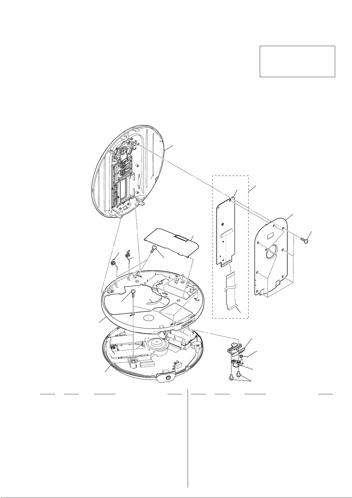
7-1. UPPER LID AND CABINET (INNER) SECTION
3
SWITCH
board
The components identified by mark
0 or dotted line with mark 0 are
critical for safety.
Replace only with part number
specified.
6
8
1
2
5
15
5
10
cabinet lower section
Ref. No. Part No. Description Remark
12-699-871-01 SPRING (L)
22-699-872-01 SPRING (R)
3 X-2159-378-1 LID SUB ASSY, UPPER (for SILVER) (NE240)
3 X-2159-381-1 LID SUB ASSY, UPPER (for BLACK) (NE240)
3 X-2159-385-1 LID SUB ASSY (S), UPPER (for SILVER)
(NE241)
3 X-2159-386-1 LID SUB ASSY (B), UPPER (for BLACK)
3 X-2176-011-1 LID SUB ASSY (B), UPPER (for BLACK)
42-699-864-01 LID, BATTERY CASE (SILVER)
42-699-864-11 LID, BATTERY CASE (BLACK)
53-254-070-11 SCREW
6 A-1209-616-A SWITCH BOARD, COMPLETE
(NE241: AEP)
(NE241CK)
4
9
7
11
12
13
14
Ref. No. Part No. Description Remark
7 1-833-573-11 CABLE, FLEXIBLE FLAT
8 2-699-865-01 COVER (LID, UPPER) (SILVER)
8 2-699-865-11 COVER (LID, UPPER) (BLACK)
9 3-254-014-11 SCREW
10 2-699-855-01 CABINET (MIDDLE) (SILVER)
10 2-699-855-11 CABINET (MIDDLE) (BLACK)
11 2-699-862-01 KNOB (OPEN) (SILVER)
11 2-699-862-11 KNOB (OPEN) (BLACK)
12 2-187-914-01 SPRING (OPEN)
13 2-187-913-01 LEVER (OPEN)
14 3-034-792-11 SCREW, TAPPING (B2.0)
15 2-895-894-01 CUSHION (CDM)
17
D-NE240/NE241/NE241CK
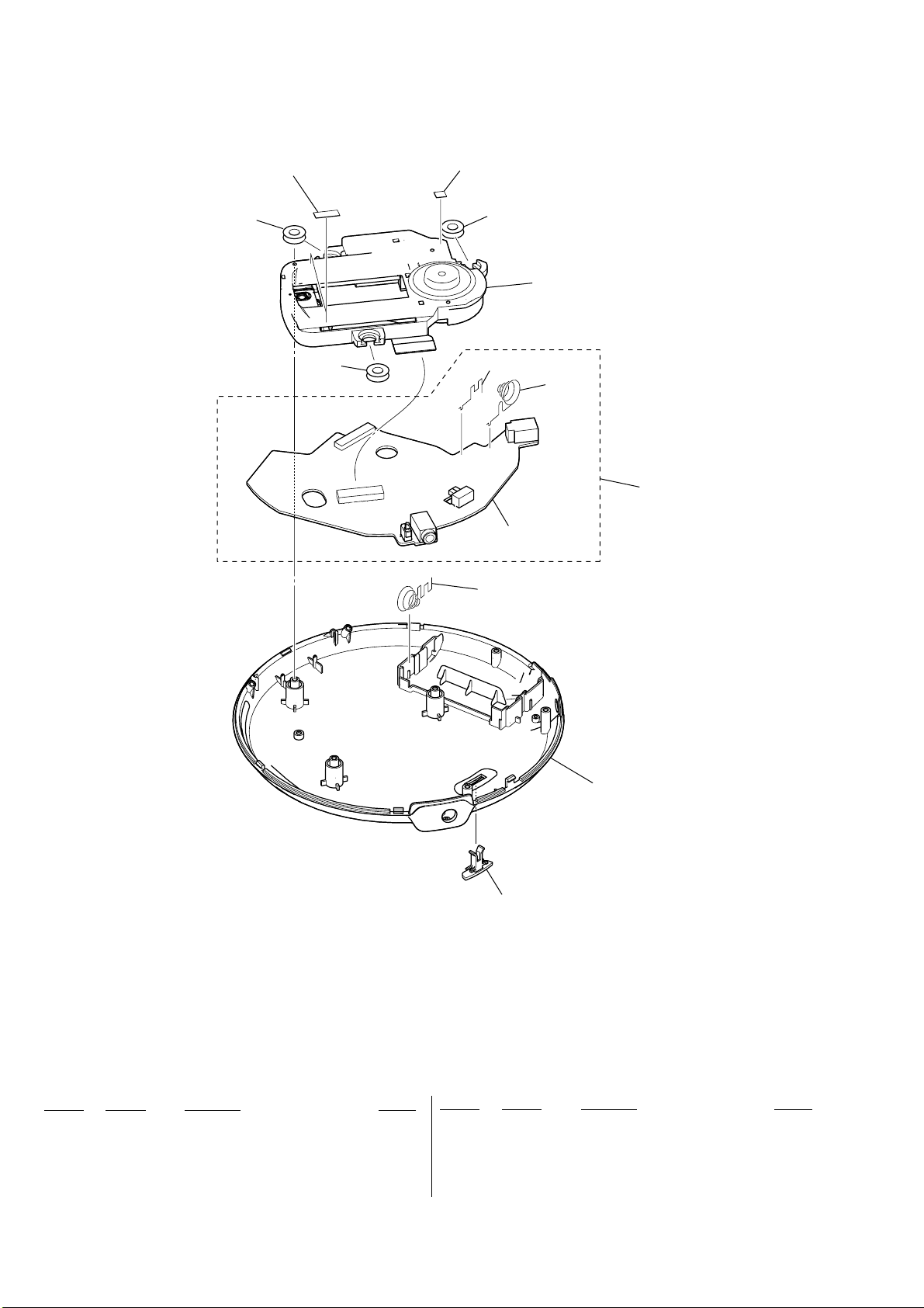
7-2. CABINET LOWER SECTION
not supplied
52
52
not supplied
52
53
54
56
55
MAIN board
51
Ref. No. Part No. Description Remark
51 2-699-869-01 TERMINAL (RELAY), BATTERY
52 3-245-331-02 INSULATOR
053 A-1112-193-A CDM-3525A (CD MECHANISM)
54 2-699-867-01 TERMINAL (+), BATTERY
55 A-1209-048-A MAIN PC BOARD ASSY
57
58
Ref. No. Part No. Description Remark
56 2-699-868-01 TERMINAL (-), BATTERY
57 2-699-856-01 CABINET (LOWER) (SILVER)
57 2-699-856-11 CABINET (LOWER) (BLACK)
58 2-699-863-01 KNOB (HOLD) (SILVER)
58 2-699-863-11 KNOB (HOLD) (BLACK)
18

SECTION 8
ELECTRICAL PARTS LIST
D-NE240/NE241/NE241CK
MAIN
NOTE:
• Due to standardization, replacements in the
parts list may be different from the parts
specified in the diagrams or the components
used on the set.
• -XX and -X mean standardized parts, so they
may have some difference from the original
one.
• RESISTORS
All resistors are in ohms.
METAL: Metal-film resistor.
METAL OXIDE: Metal oxide-film resistor.
F: nonflammable
• Abbreviation
E92: 120 V AC area in E model
MX: Mexican model
Ref. No. Part No. Description Remark Ref. No. Part No. Description Remark
A-1209-048-A MAIN BOARD, COMPLETE
*********************
2-699-867-01 TERMINAL (+), BATTERY
2-699-868-01 TERMINAL (–), BATTERY
< CAPACITOR >
C101 1-162-966-11 CERAMIC CHIP 0.0022uF 10% 50V
C102 1-162-964-11 CERAMIC CHIP 0.001uF 10% 50V
C104 1-124-635-00 ELECT 220uF 20% 6.3V
C105 1-135-834-11 CERAMIC CHIP 2.2uF 6.3V
C106 1-115-467-11 CERAMIC CHIP 0.22uF 10% 10V
C108 1-162-962-11 CERAMIC CHIP 470PF 10% 50V
C110 1-162-964-11 CERAMIC CHIP 0.001uF 10% 50V
C201 1-162-966-11 CERAMIC CHIP 0.0022uF 10% 50V
C202 1-162-964-11 CERAMIC CHIP 0.001uF 10% 50V
C204 1-124-635-00 ELECT 220uF 20% 6.3V
C205 1-135-834-11 CERAMIC CHIP 2.2uF 6.3V
C206 1-115-467-11 CERAMIC CHIP 0.22uF 10% 10V
C208 1-162-962-11 CERAMIC CHIP 470PF 10% 50V
C210 1-162-964-11 CERAMIC CHIP 0.001uF 10% 50V
C301 1-107-826-11 CERAMIC CHIP 0.1uF 10% 16V
C303 1-125-837-11 CERAMIC CHIP 1uF 10% 6.3V
C304 1-126-382-11 ELECT 100uF 20% 16V
C305 1-126-513-11 ELECT 47uF 20% 6.3V
C320 1-165-176-11 CERAMIC CHIP 0.047uF 10% 16V
C321 1-165-176-11 CERAMIC CHIP 0.047uF 10% 16V
C322 1-165-176-11 CERAMIC CHIP 0.047uF 10% 16V
C323 1-165-176-11 CERAMIC CHIP 0.047uF 10% 16V
C324 1-117-863-11 CERAMIC CHIP 0.47uF 10% 6.3V
C401 1-100-352-11 CERAMIC CHIP 1uF 20% 16V
C402 1-162-970-11 CERAMIC CHIP 0.01uF 10% 25V
C403 1-164-156-11 CERAMIC CHIP 0.1uF 25V
C404 1-126-791-11 ELECT 10uF 20% 35V
C405 1-162-964-11 CERAMIC CHIP 0.001uF 10% 50V
C406 1-164-156-11 CERAMIC CHIP 0.1uF 25V
C407 1-112-342-91 CERAMIC CHIP 10uF 20% 10V
C408 1-124-635-00 ELECT 220uF 20% 6.3V
C409 1-126-791-11 ELECT 10uF 20% 35V
C410 1-107-826-11 CERAMIC CHIP 0.1uF 10% 16V
C411 1-162-962-11 CERAMIC CHIP 470PF 10% 50V
C412 1-115-156-11 CERAMIC CHIP 1uF 10V
C413 1-164-227-11 CERAMIC CHIP 0.022uF 10% 25V
C416 1-162-923-11 CERAMIC CHIP 47PF 5% 50V
• Items marked “*” are not stocked since they
are seldom required for routine service.
Some delay should be anticipated when
ordering these items.
• SEMICONDUCTORS
In each case, u: µ, for example:
uA... : µA... uPA... : µPA...
uPB... : µPB... uPC... : µPC...
uPD... : µPD...
• CAPACITORS
uF: µF
• COILS
uH: µH
C417 1-107-826-11 CERAMIC CHIP 0.1uF 10% 16V
C419 1-124-635-00 ELECT 220uF 20% 6.3V
C420 1-119-941-41 ELECT 470uF 20% 6.3V
C421 1-115-467-11 CERAMIC CHIP 0.22uF 10% 10V
C428 1-164-227-11 CERAMIC CHIP 0.022uF 10% 25V
C431 1-100-352-11 CERAMIC CHIP 1uF 20% 16V
C601 1-126-513-11 ELECT 47uF 20% 6.3V
C602 1-126-513-11 ELECT 47uF 20% 6.3V
C603 1-162-970-11 CERAMIC CHIP 0.01uF 10% 25V
C604 1-107-826-11 CERAMIC CHIP 0.1uF 10% 16V
C605 1-164-156-11 CERAMIC CHIP 0.1uF 25V
C606 1-107-826-11 CERAMIC CHIP 0.1uF 10% 16V
C607 1-126-513-11 ELECT 47uF 20% 6.3V
C609 1-162-966-11 CERAMIC CHIP 0.0022uF 10% 50V
C610 1-126-794-11 ELECT 4.7uF 20% 50V
C611 1-115-467-11 CERAMIC CHIP 0.22uF 10% 10V
C612 1-164-156-11 CERAMIC CHIP 0.1uF 25V
C615 1-162-966-11 CERAMIC CHIP 0.0022uF 10% 50V
C618 1-162-962-11 CERAMIC CHIP 470PF 10% 50V
C619 1-107-826-11 CERAMIC CHIP 0.1uF 10% 16V
C620 1-164-156-11 CERAMIC CHIP 0.1uF 25V
C623 1-119-941-41 ELECT 470uF 20% 6.3V
C624 1-107-826-11 CERAMIC CHIP 0.1uF 10% 16V
C625 1-125-838-11 CERAMIC CHIP 2.2uF 10% 6.3V
C626 1-162-970-11 CERAMIC CHIP 0.01uF 10% 25V
C627 1-100-507-91 CERAMIC CHIP 4.7uF 20% 6.3V
C628 1-126-791-11 ELECT 10uF 20% 35V
C629 1-135-834-11 CERAMIC CHIP 2.2uF 6.3V
C630 1-126-791-11 ELECT 10uF 20% 35V
C631 1-107-826-11 CERAMIC CHIP 0.1uF 10% 16V
C632 1-100-966-91 CERAMIC CHIP 10uF 20% 10V
C633 1-107-826-11 CERAMIC CHIP 0.1uF 10% 16V
C634 1-125-837-11 CERAMIC CHIP 1uF 10% 6.3V
C637 1-107-826-11 CERAMIC CHIP 0.1uF 10% 16V
C640 1-100-507-91 CERAMIC CHIP 4.7uF 20% 6.3V
C642 1-100-352-11 CERAMIC CHIP 1uF 20% 16V
C802 1-162-970-11 CERAMIC CHIP 0.01uF 10% 25V
C805 1-107-826-11 CERAMIC CHIP 0.1uF 10% 16V
C806 1-107-826-11 CERAMIC CHIP 0.1uF 10% 16V
C807 1-115-156-11 CERAMIC CHIP 1uF 10V
C808 1-115-156-11 CERAMIC CHIP 1uF 10V
C809 1-164-156-11 CERAMIC CHIP 0.1uF 25V
C810 1-126-514-11 ELECT 22uF 20% 16V
The components identified by mark
0 or dotted line with mark 0 are
critical for safety.
Replace only with part number
specified.
When indicating parts by reference
number, please include the board.
19

D-NE240/NE241/NE241CK
MAIN
Ref. No. Part No. Description Remark Ref. No. Part No. Description Remark
C811 1-107-826-11 CERAMIC CHIP 0.1uF 10% 16V
C812 1-162-962-11 CERAMIC CHIP 470PF 10% 50V
C813 1-162-962-11 CERAMIC CHIP 470PF 10% 50V
C814 1-162-962-11 CERAMIC CHIP 470PF 10% 50V
C818 1-107-826-11 CERAMIC CHIP 0.1uF 10% 16V
C871 1-107-826-11 CERAMIC CHIP 0.1uF 10% 16V
< COMPOSITION CIRCUIT BLOCK >
CB414 1-112-557-11 CERAMIC CHIP 0.022uF 20% 16V
< CONNECTOR >
CN501 1-774-975-51 CONNECTOR, FFC/FPC 16P
CN801 1-573-370-51 CONNECTOR, FFC/FPC (ZIF) 30P
Q320 8-729-051-23 TRANSISTOR 2SA2018TL
Q321 6-551-375-01 TRANSISTOR UMB2N-TN
Q322 6-551-395-01 TRANSISTOR UMH8N-TR
Q323 6-551-395-01 TRANSISTOR UMH8N-TR
Q324 6-551-395-01 TRANSISTOR UMH8N-TR
Q401 8-729-106-60 TRANSISTOR 2SB1115A-YQ
Q402 6-551-395-01 TRANSISTOR UMH8N-TR
Q403 6-550-364-01 TRANSISTOR 2SD2652T106
Q404 6-550-364-01 TRANSISTOR 2SD2652T106
Q601 8-729-602-36 TRANSISTOR 2SA1602-F
Q602 8-729-028-97 TRANSISTOR DTC114TUA-T106
< TRANSISTOR >
< DIODE >
D401 8-719-422-58 DIODE MA8062
D402 8-719-085-43 DIODE MA2YD2300LS0
D403 8-719-085-43 DIODE MA2YD2300LS0
D404 8-719-083-82 DIODE UDZS-TE17-12B
D406 8-719-083-82 DIODE UDZS-TE17-12B
D803 8-719-404-50 DIODE MA111-TX
< FUSE >
0F401 1-576-415-21 FUSE (2A/32V)
0F402 1-576-415-21 FUSE (2A/32V)
< FERRITE BEAD/JUMPER RESISTOR >
FB301 1-414-813-11 FERRITE, EMI (SMD) (2012)
FB401 1-216-864-11 SHORT CHIP 0
FB602 1-414-760-21 FERRITE, EMI (SMD) (1608)
FB605 1-414-760-21 FERRITE, EMI (SMD) (1608)
FB801 1-414-760-21 FERRITE, EMI (SMD) (1608)
< IC >
IC301 8-759-588-61 IC BH3544F-FE2
IC401 6-704-047-01 IC BH6575FV-E2
IC601 6-709-383-01 IC BU9541JKV
IC602 6-709-459-01 IC M12L16161A-7T (J)
IC603 6-705-807-01 IC BH15FB1WG
IC801 6-805-927-02 IC BU18704-S1
IC802 6-704-001-01 IC BR24L02F-WE2
< JACK >
J301 1-819-363-11 JACK, HEADPHONE (i)
J401 1-819-364-11 JACK, DC (POLARITY UNIFIED TYPE)
< COIL >
L101 1-469-152-11 FERRITE, EMI (SMD) (2012)
L201 1-469-152-11 FERRITE, EMI (SMD) (2012)
L401 1-457-095-11 INDUCTOR 330uH
L402 1-457-096-11 INDUCTOR 165uH
L403 1-400-945-11 INDUCTOR 10uH
L404 1-469-670-21 FERRITE, EMI (SMD) (2012)
L405 1-469-670-21 FERRITE, EMI (SMD) (2012)
L406 1-400-145-21 INDUCTOR 47uH
L407 1-400-145-21 INDUCTOR 47uH
(DC IN 4.5V)
< RESISTOR/FERRITE BEAD >
R101 1-216-797-11 METAL CHIP 10 5% 1/10W
R102 1-216-789-11 METAL CHIP 2.2 5% 1/10W
R103 1-216-837-11 METAL CHIP 22K 5% 1/10W
R111 1-216-797-11 METAL CHIP 10 5% 1/10W
R201 1-216-797-11 METAL CHIP 10 5% 1/10W
R202 1-216-789-11 METAL CHIP 2.2 5% 1/10W
R203 1-216-837-11 METAL CHIP 22K 5% 1/10W
R211 1-216-797-11 METAL CHIP 10 5% 1/10W
R304 1-216-857-11 METAL CHIP 1M 5% 1/10W
R305 1-216-849-11 METAL CHIP 220K 5% 1/10W
R320 1-216-813-11 METAL CHIP 220 5% 1/10W
R321 1-216-813-11 METAL CHIP 220 5% 1/10W
R322 1-216-857-11 METAL CHIP 1M 5% 1/10W
R323 1-216-857-11 METAL CHIP 1M 5% 1/10W
R326 1-216-825-11 METAL CHIP 2.2K 5% 1/10W
R327 1-216-825-11 METAL CHIP 2.2K 5% 1/10W
R328 1-216-857-11 METAL CHIP 1M 5% 1/10W
R329 1-216-857-11 METAL CHIP 1M 5% 1/10W
R401 1-216-845-11 METAL CHIP 100K 5% 1/10W
R402 1-216-837-11 METAL CHIP 22K 5% 1/10W
R403 1-216-821-11 METAL CHIP 1K 5% 1/10W
R404 1-216-809-11 METAL CHIP 100 5% 1/10W
R405 1-218-873-11 METAL CHIP 12K 0.5% 1/10W
R406 1-216-833-11 METAL CHIP 10K 5% 1/10W
R407 1-218-881-11 METAL CHIP 27K 0.5% 1/10W
R410 1-218-446-11 METAL CHIP 1 5% 1/10W
R414 1-216-797-11 METAL CHIP 10 5% 1/10W
R415 1-216-821-11 METAL CHIP 1K 5% 1/10W
R416 1-216-837-11 METAL CHIP 22K 5% 1/10W
R417 1-216-845-11 METAL CHIP 100K 5% 1/10W
R418 1-216-841-11 METAL CHIP 47K 5% 1/10W
R419 1-216-837-11 METAL CHIP 22K 5% 1/10W
R422 1-216-841-11 METAL CHIP 47K 5% 1/10W
R602 1-216-789-11 METAL CHIP 2.2 5% 1/10W
R603 1-216-793-11 METAL CHIP 4.7 5% 1/10W
R604 1-216-845-11 METAL CHIP 100K 5% 1/10W
R606 1-216-849-11 METAL CHIP 220K 5% 1/10W
R613 1-216-843-11 METAL CHIP 68K 5% 1/10W
R614 1-216-817-11 METAL CHIP 470 5% 1/10W
R615 1-216-843-11 METAL CHIP 68K 5% 1/10W
R617 1-216-809-11 METAL CHIP 100 5% 1/10W
R618 1-216-857-11 METAL CHIP 1M 5% 1/10W
20

D-NE240/NE241/NE241CK
SWITCHMAIN
Ref. No. Part No. Description Remark Ref. No. Part No. Description Remark
R619 1-216-845-11 METAL CHIP 100K 5% 1/10W
R621 1-414-760-21 FERRITE, EMI (SMD) (1608)
R622 1-216-813-11 METAL CHIP 220 5% 1/10W
R624 1-216-845-11 METAL CHIP 100K 5% 1/10W
R626 1-216-813-11 METAL CHIP 220 5% 1/10W
R804 1-216-864-11 SHORT CHIP 0
R810 1-216-857-11 METAL CHIP 1M 5% 1/10W
R811 1-216-845-11 METAL CHIP 100K 5% 1/10W
C819 1-162-962-11 CERAMIC CHIP 470PF 10% 50V
C820 1-162-962-11 CERAMIC CHIP 470PF 10% 50V
A-1209-616-A SWITCH BOARD, COMPLETE
***********************
1-833-573-11 CABLE, FLEXIBLE FLAT
< CAPACITOR >
R812 1-216-845-11 METAL CHIP 100K 5% 1/10W
R817 1-216-833-11 METAL CHIP 10K 5% 1/10W
R818 1-216-845-11 METAL CHIP 100K 5% 1/10W
R821 1-216-845-11 METAL CHIP 100K 5% 1/10W
R823 1-216-821-11 METAL CHIP 1K 5% 1/10W
R827 1-216-853-11 METAL CHIP 470K 5% 1/10W
R828 1-216-825-11 METAL CHIP 2.2K 5% 1/10W
R829 1-216-845-11 METAL CHIP 100K 5% 1/10W
R835 1-414-760-21 FERRITE, EMI (SMD) (1608)
R847 1-216-825-11 METAL CHIP 2.2K 5% 1/10W
R848 1-216-825-11 METAL CHIP 2.2K 5% 1/10W
R856 1-216-817-11 METAL CHIP 470 5% 1/10W
< COMPOSITION CIRCUIT BLOCK >
RB301 1-233-787-11 RES, NETWORK 1K (1608)
RB303 1-233-679-11 RES, NETWORK (1608) 470
RB304 1-233-679-11 RES, NETWORK (1608) 470
RB305 1-233-790-91 RES, NETWORK 22K (1608)
RB330 1-233-791-91 RES, NETWORK 47K (1608)
RB331 1-233-787-11 RES, NETWORK 1K (1608)
RB601 1-233-789-11 RES, NETWORK 10K (1608)
RB602 1-233-789-11 RES, NETWORK 10K (1608)
RB620 1-233-789-11 RES, NETWORK 10K (1608)
RB801 1-233-789-11 RES, NETWORK 10K (1608)
RB803 1-233-789-11 RES, NETWORK 10K (1608)
RB806 1-233-791-91 RES, NETWORK 47K (1608)
RB810 1-236-908-11 RES, CHIP NETWORK 10K (3216)
RB811 1-236-908-11 RES, CHIP NETWORK 10K (3216)
RB812 1-236-908-11 RES, CHIP NETWORK 10K (3216)
< CONNECTOR >
CN802 1-573-939-51 CONNECTOR, FFC/FPC (ZIF) 30P
< RESISTOR >
R849 1-216-825-11 METAL CHIP 2.2K 5% 1/10W
R850 1-216-829-11 METAL CHIP 4.7K 5% 1/10W
R851 1-216-837-11 METAL CHIP 22K 5% 1/10W
R852 1-216-825-11 METAL CHIP 2.2K 5% 1/10W
R853 1-216-829-11 METAL CHIP 4.7K 5% 1/10W
R854 1-216-837-11 METAL CHIP 22K 5% 1/10W
< SWITCH >
S801 1-786-650-21 SWITCH, TACTILE (u, ENTER)
S802 1-786-650-21 SWITCH, TACTILE (>, FOLDER +)
S803 1-786-650-21 SWITCH, TACTILE (., FOLDER –)
S804 1-786-650-21 SWITCH, TACTILE (VOL +)
S805 1-786-650-21 SWITCH, TACTILE (VOL –)
S806 1-786-650-21 SWITCH, TACTILE (GROUP)
S807 1-786-650-21 SWITCH, TACTILE (STOP, x)
S808 1-786-650-21 SWITCH, TACTILE (SOUND, AVLS)
S809 1-786-650-21 SWITCH, TACTILE (P MODE, F)
************************************************************
MISCELLANEOUS
**************
0 53 A-1112-193-A CDM-3525A (CD MECHANISM)
************************************************************
RB813 1-236-908-11 RES, CHIP NETWORK 10K (3216)
RB814 1-236-908-11 RES, CHIP NETWORK 10K (3216)
RB815 1-236-908-11 RES, CHIP NETWORK 10K (3216)
< SWITCH >
S811 1-570-953-11 SWITCH, PUSH (1 KEY) (OPEN/CLOSE DETECT)
S812 1-786-864-11 SWITCH, SLIDE (HOLD)
< CAPACITOR/VARISTOR >
VDR101 1-162-966-11 CERAMIC CHIP 0.0022uF 10% 50V
VDR201 1-162-966-11 CERAMIC CHIP 0.0022uF 10% 50V
VDR418 1-801-864-21 VARISTOR, CHIP (1608)
VDR801 1-801-923-11 VARISTOR, CHIP (1608)
VDR802 1-801-923-11 VARISTOR, CHIP (1608)
< VIBRATOR >
X601 1-813-590-11 VIBRATOR, CERAMIC (16.9344MHz)
************************************************************
21

D-NE240/NE241/NE241CK
Ref. No. Part No. Description Remark Ref. No. Part No. Description Remark
ACCESSORIES
************
1-251-824-41 CONNECTING PACK, CAR (CPA-7) (NE241CK)
0 1-479-496-21 ADAPTOR, AC (AC-ES457K)
0 1-479-497-21 ADAPTOR, AC (AC-ES457K) (NE241: AEP)
1-542-673-12 HEADPHONE (MDR-J0Z1LP/BC19)
1-542-697-31 HEADPHONE (MDR-E706) (NE240/NE241: AEP)
1-792-970-41 CORD, CAR BATTERY (DCC-E2455) (NE241CK)
2-892-695-21 MANUAL, INSTRUCTION (ENGLISH, FRENCH,
GERMAN, ITALIAN) (NE240/NE241: AEP)
2-892-695-31 MANUAL, INSTRUCTION (SPANISH, DUTCH,
2-892-695-42 MANUAL, INSTRUCTION (HUNGARIAN,
POLISH, CZECH, SLOVAKIAN, RUSSIAN)
2-892-695-51 MANUAL, INSTRUCTION (ARABIC)
(NE241: MX, E92/NE241CK)
(NE241: MX, E92/NE241CK)
PORTUGUESE, SWEDISH, FINNISH)
(NE240/NE241: AEP)
(NE240/NE241: AEP)
(NE241: AEP)
2-892-695-61 MANUAL, INSTRUCTION (ENGLISH)
2-892-695-81 MANUAL, INSTRUCTION (SPANISH)
2-892-695-91 MANUAL, INSTRUCTION (PORTUGUESE)
2-892-696-21 MANUAL, INSTRUCTION (SPANISH) (NE241CK)
3-234-573-01 TAPE, MAGIC (NE241CK)
(NE241: E92)
(NE241: MX, E92)
(NE241: E92)
22

MEMO
D-NE240/NE241/NE241CK
23

D-NE240/NE241/NE241CK
REVISION HISTORY
Clicking the version allows you to jump to the revised page.
Also, clicking the version at the upper right on the revised page allows you to jump to the next revised
page.
Ver. Date Description of Revision
1.0 2006.10 New
2
 Loading...