

Sony D-E200, D-E201, D-E206CK, D-E251 Service manual
D-E200/E201/E206CK/E251
SERVICE MANUAL
Ver 1.3 2001.06
With SUPPLEMENT-1
(9-927-666-81)
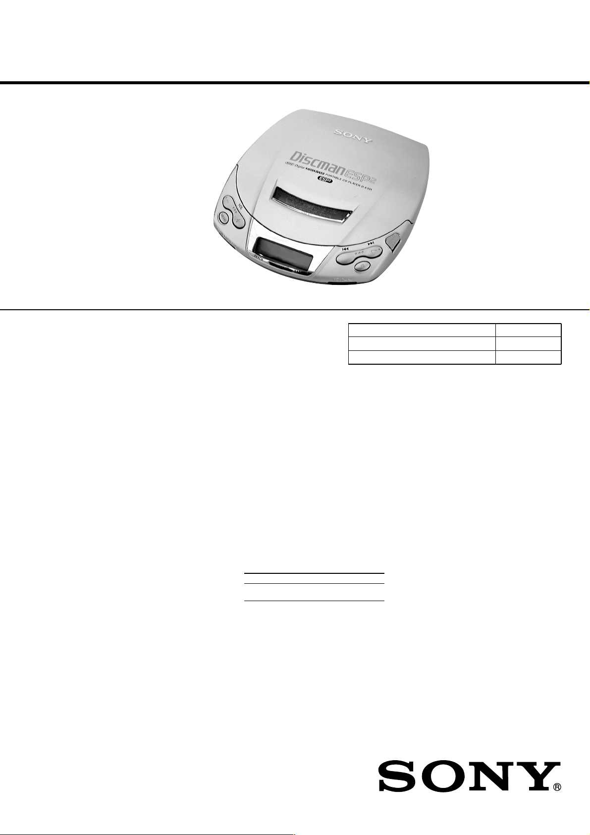
(Photo: D-E201 (Silver))
SPECIFICATIONS
CD player
System
Compact disc digital audio system
Laser diode properties
Material: GaAlAs
Wavelength: λ = 780 nm
Emission duration: Continuous
Laser output: Less than 44.6 µW (This output
is the value measured at a distance of 200 mm
from the objective lens surface on the optical
pick-up block with 7 mm aperture.)
Error correction
Sony Super Strategy Cross Interleave Reed
Solomon Code
D-A conversion
1-bit quartz time-axis control
Frequency response
20 - 20,000 Hz +1/–3 dB
(measured by EIAJ CP-307)
Output (at 4.5 V input level)
Headphones (stereo minijack)
Approx. 15 mW + Approx. 15 mW
at 16 ohms
General
Power requirements
For the area code of the model you purchased,
check the upper left side of the bar code on the
package.
• Two LR6 (size AA) batteries: 3 V DC
• AC power adaptor (DC IN 4.5 V jack):
US/CND/E92/MX model: 120 V, 60Hz
AEP/FR/EE/E13/G model: 220 - 230 V,
50/60Hz
UK model: 230 - 240 V, 50 Hz
EA model: 110 - 240 V, 50/60 Hz
AUS model: 240 V, 50 Hz
E33 model: 100 - 240 V, 50/60 Hz
HK model: 220 V, 50/60 Hz
CH/AR model: 220 V, 50 Hz
• Sony CPM-300P mount plate for use on car
battery: 4.5 V DC
Battery life (approx. hours) (EIAJ*)
Battery life varies depending on how the player is
used.
ESP OFF ESP ON
Two alkaline 15 14
batteries LR6
* Measured value by the standard of EIAJ
(Electronic Industries Association of Japan).
(When the unit is used on a flat and stable place.)
US Model
D-E200/E206CK/E251
AEP Model
D-E200/E201/E206CK/E251
Canadian Model
UK Model
E Model
Australian Model
D-E201/E206CK
Chinese Model
D-E201
Model Name Using Similar Mechanism D-190/191
CD Mechanism Type CDM-2811AAC
Optical Pick-up Name DAX-11A
Dimensions (w/h/d) (without projecting
parts and controls)
Approx. 131 × 28 × 148 mm
1/4 × 1 1/9 × 5 4/5 in.)
(5
Mass
Approx. 220 g (7.8 oz.)
Operating temperature
5°C - 35°C (41°F - 95°C)
Supplied accessories
For the area code of the model you purchased,
check the upper left side of the bar code on the
package.
D-E200
Headphones/earphones (1)
D-E201
AC power adaptor (1)
Headphones/earphones (1)
D-E251
AC power adaptor (1)
Headphones/earphones (1)
– Continued on next page –
9-927-666-13
2001F0400-1
© 2001.6
PORTABLE CD PLAYER
Sony Corporation
Personal Audio Company
Shinagawa Tec Service Manual Production Group
– 1 –
D-E206CK
AC power adaptor (1)
Headphones/earphones (1)
Car connecting pack (1)
Car battery cord (1)
Spiral tube (1)
Velcro tape (2)
Design and specifications are subject to change
without notice.
For US customers
AC power adaptor supplied is not intended to be
serviced. Should the AC power adaptor cease to
function in its intended manner, during the
warranty period, the adaptor should be returned
to your nearest Sony Service Center or Sony
Authorized Repair Center for replacement, or
after warranty period, it should be discarded.
• Abbreviation
AR : Argentine model
AUS : Australian model
CH : Chinese model
CND : Canadian model
E13 : AC 220-230V area in E model
E33 : AC 100-240V area in E model
E92 : AC 120V area in E model
EA : Saudi Arabia model
EE : East European model
FR : French model
G : German model
HK : Hong Kong model
MX : Mexican model
TABLE OF CONTENTS
1. SERVICE NOTE ................................................................3
2. GENERAL
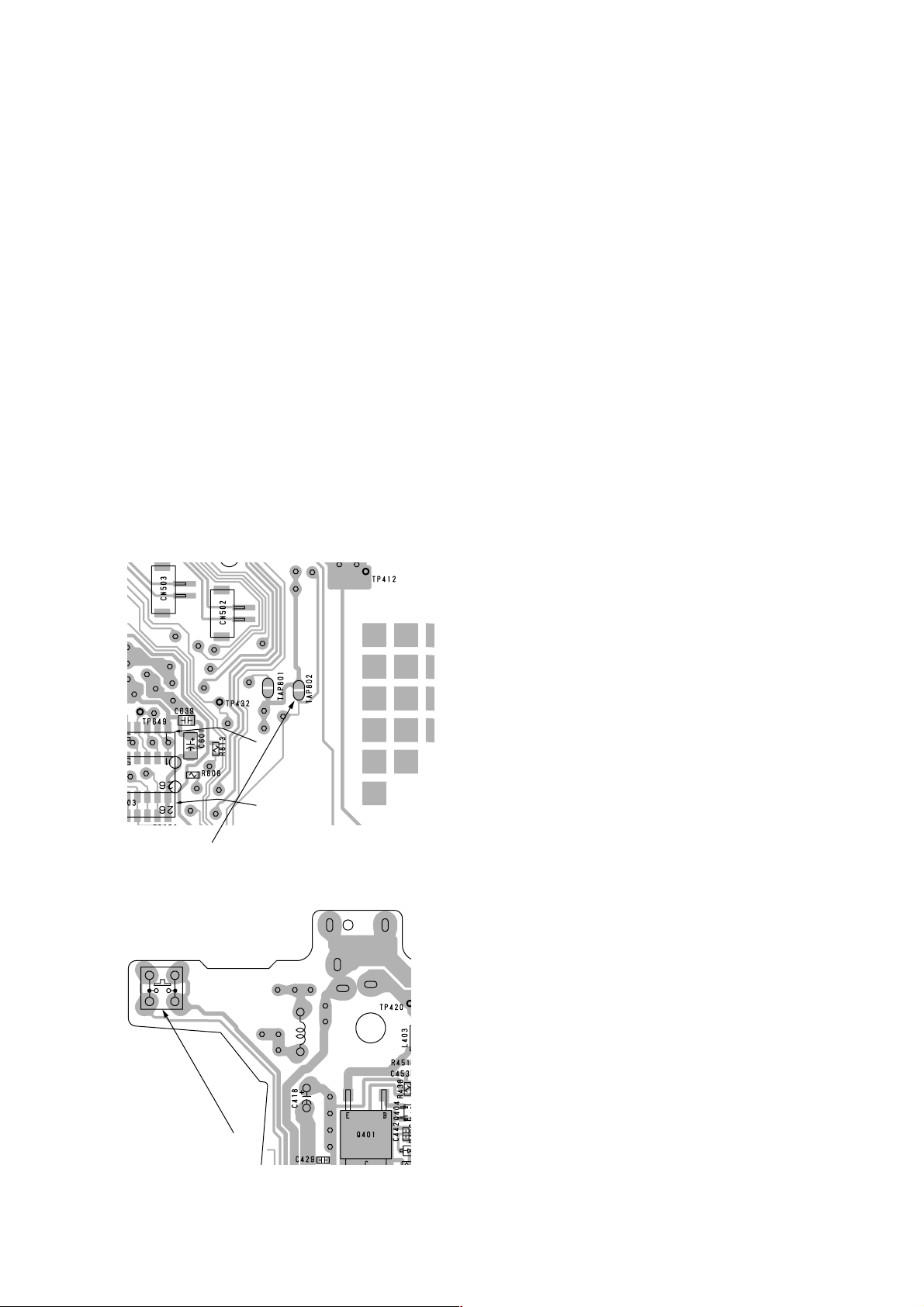
Playing a CD right away! ........................................................4
3. DISASSEMBLY
3-1. Cabinet (Lower) Sub Assy .................................................. 6
3-2. Main Board, MD Assy ........................................................ 6
4. ELECTRICAL ADJUSTMENTS
4-1. Focus Bias Check ................................................................ 7
5. DIAGRAMS
5-1. IC Pin Description............................................................... 8
5-2. Block Diagram –CD Section–........................................... 10
5-3. Block Diagram –Power Supply Section–.......................... 13
5-4. Printed Wiring Boards –Main Section– ............................ 15
5-5. Schematic Diagram –Main Section (1/2)– ........................ 19
5-6. Schematic Diagram –Main Section (2/2)– ........................ 21
5-7. IC Block Diagrams............................................................ 23
6. EXPLODED VIEWS
6-1. Cabinet (Upper) Section.................................................... 25
6-2. Cabinet (Lower) Section ................................................... 26
6-3. CD Mechanism Deck Section (CDM-2811AAC)............. 27
7. ELECTRICAL PARTS LIST.........................................28
CAUTION
Use of controls or adjustments or performance of procedures other than those specified herein may result in hazardous radiation exposure.
This Compact Disc player is
classified as a CLASS 1
LASER product.
The CLASS 1 LASER
PRODUCT table is located
on the bottom exterior.
Flexible Circuit Board Repairing
• Keep the temperature of the soldering iron around 270°C during
repairing.
• Do not touch the soldering iron on the same conductor of the
circuit board (within 3 times).
• Be careful not to apply force on the conductor when soldering
or unsoldering.
Notes on Chip Component Replacement
• Never reuse a disconnected chip component.
• Notice that the minus side of a tantalum capacitor may be
damaged by heat.
SAFETY-RELATED COMPONENT WARNING!!
COMPONENTS IDENTIFIED BY MARK 0 OR DOTTED LINE
WITH MARK 0 ON THE SCHEMATIC DIAGRAMS AND IN
THE PARTS LIST ARE CRITICAL TO SAFE OPERATION.
REPLACE THESE COMPONENTS WITH SONY P ARTS WHOSE
P ART NUMBERS APPEAR AS SHOWN IN THIS MANU AL OR
IN SUPPLEMENTS PUBLISHED BY SONY.
ATTENTION AU COMPOSANT AYANT RAPPORT
À LA SÉCURITÉ!!
LES COMPOSANTS IDENTIFIÉS P AR UNE MARQUE 0 SUR LES
DIAGRAMMES SCHÉMA TIQUES ET LA LISTE DES PIÈCES SONT
CRITIQUES POUR LA SÉCURITÉ DE FONCTIONNEMENT. NE
REMPLACER CES COMPOSANTS QUE PAR DES PIÈCES SONY
DONT LES NUMÉROS SONT DONNÉS DANS CE MANUEL OU
DANS LES SUPPLÉMENTS PUBLIÉS PAR SONY.
– 2 –
SECTION 1
SERVICE NOTE
• NOTES ON HANDLING THE OPTICAL PICK-UP BLOCK
OR BASE UNIT
The laser diode in the optical pick-up block may suffer electrostatic breakdown because of the potential difference generated by
the charged electrostatic load, etc. on clothing and the human body .
During repair, pay attention to electrostatic breakdown and also
use the procedure in the printed matter which is included in the
repair parts.
The flexible board is easily damaged and should be handled with
care.
• NOTES ON LASER DIODE EMISSION CHECK
The laser beam on this model is concentrated so as to be focused
on the disc reflective surface by the objective lens in the optical
pick-up block. Therefo re, when checking the laser diode emission, observe from more than 30 cm away from the objectiv e lens.
• To Check the Laser Diode and Focus Searc h Operation
Open the upper panel. Turn on the power without a disc while
the main board S801 (OPEN) is ON (or T AP802 is shorted). Then,
observe the objective lens and check that the following operations are performed.
1. Scatterd light of laser beams is seen.
2. Check for vertical movements (five) of the objecti ve lens (with
movement of the PU on the inner circumference).
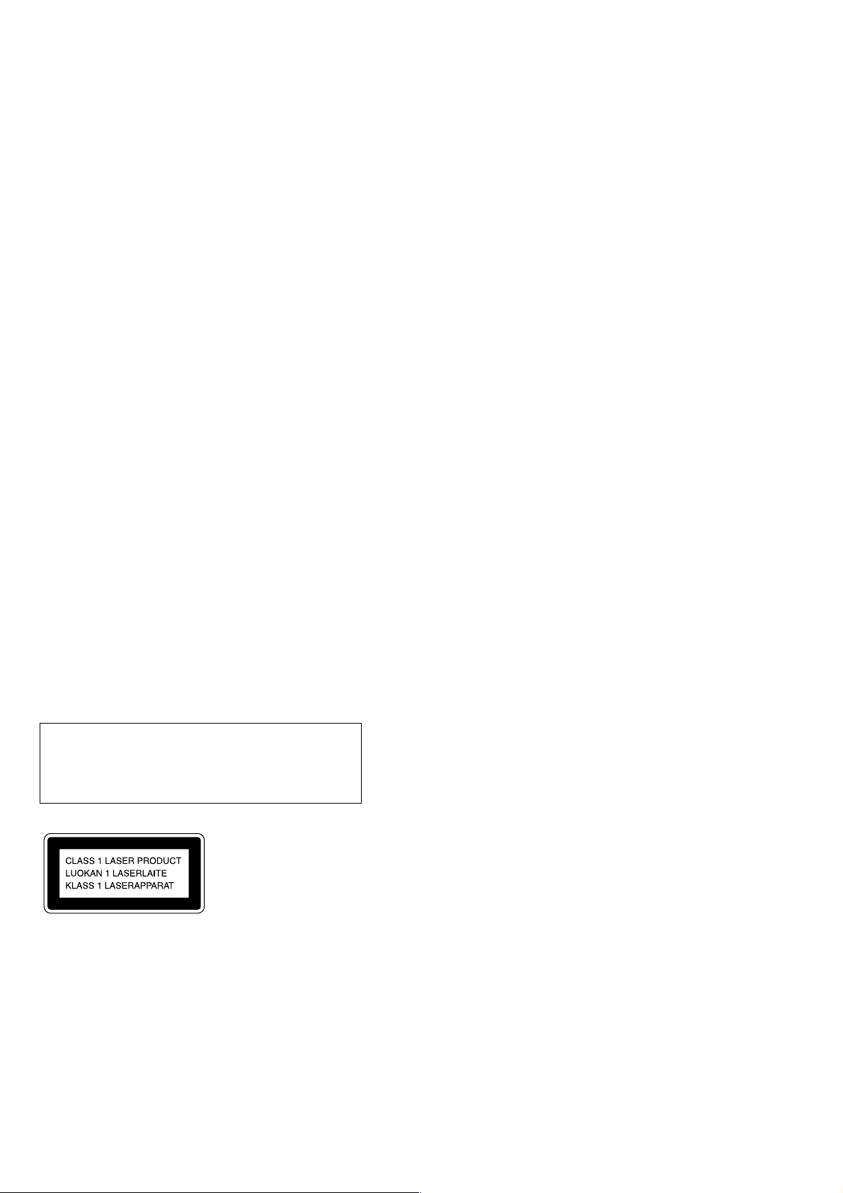
– MAIN BOARD – (SIDE A)
• Before Replacing the Optical Pick-Up Block
Please be sure to check throughly the parameters as par the “Optical Pick-Up Block Checking Procedures” (Part No.: 9-960-027-
11) issued separately before replacing the optical pick-up block.
Note and specifications required to check are given below.
• FOK output : IC601 eg pin
When checking FOK, remove the lead wire to disc motor.
When checking FOK value, remove the lead wire to disc
motor.
• RF signal P-to-P value : 0.46 - 0.66 Vp-p
• The repairing grating holder is impossible.
D-E251
D-E200/E201/E206CK
TAP802
– MAIN BOARD – (SIDE B)
S801
(OPEN)
S801
L401
– 3 –
SECTION 2
GENERAL
This section is extracted
from instruction manual.
– 4 –

– 5 –
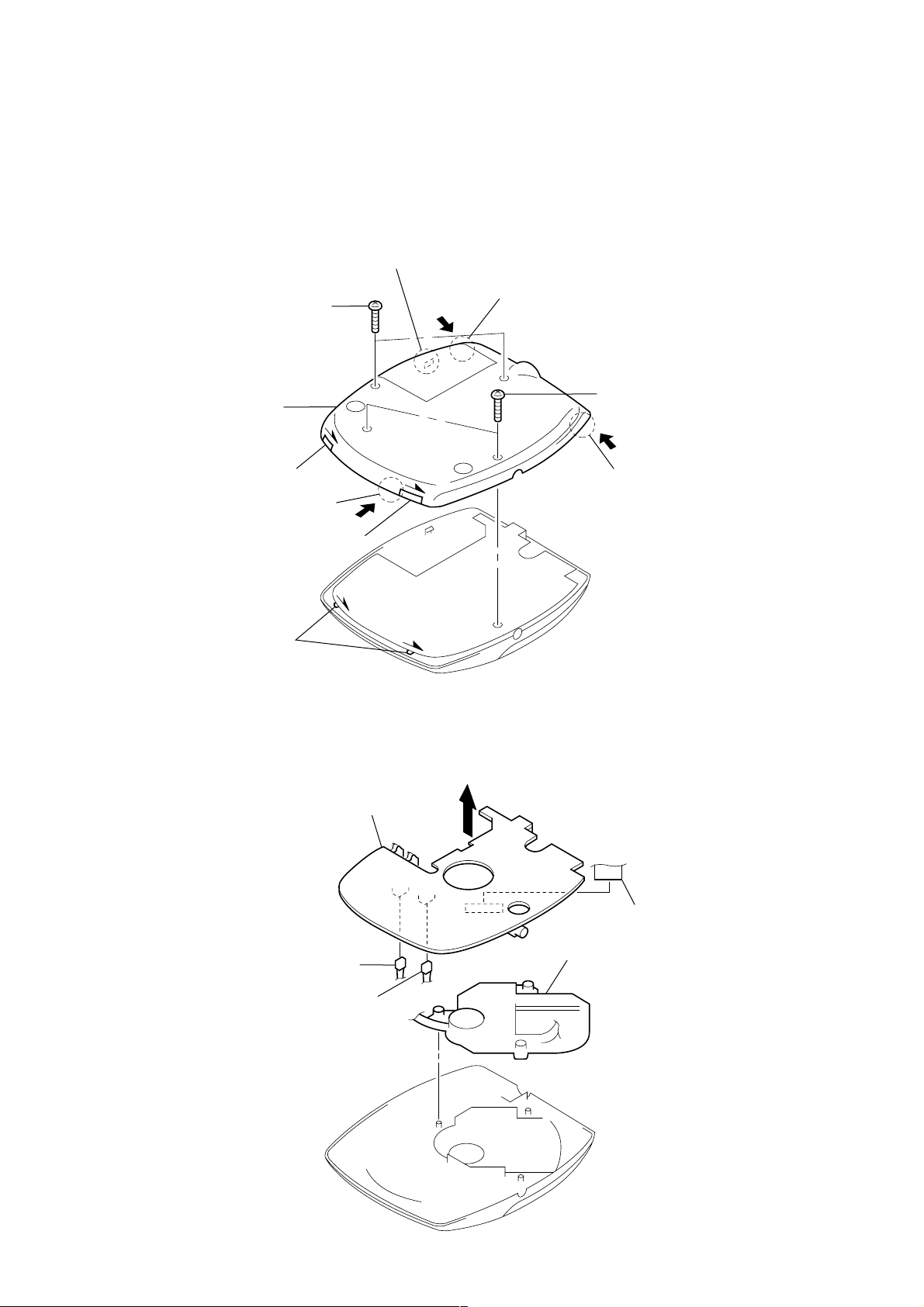
SECTION 3
DISASSEMBLY
Note : Follow the disassembly procedure in the numerical order given.
3-1. CABINET (LOWER) SUB ASSY
Note : When installing, fit the knobs (H-B) and switches.
4 claw
(Open the “lid, battery case” .)
1 screws (B2x10) (G), tapping
3 claw
7 cabinet (lower) sub assy
3-2. MAIN BOARD, MD ASSY
knob (H-B)
switches
2 screws (B2x10) (G), tapping
5 claw
6 claw
knob (H-B)
4 MAIN board
2 CN502
3 CN503
1 CN501
5 MD assy
– 6 –
SECTION 4
ELECTRICAL ADJUSTMENTS
SECTION 5
DIAGRAMS
CD section adjustments are done automatically in this set.
In case of operation check, confirm that focus bias.
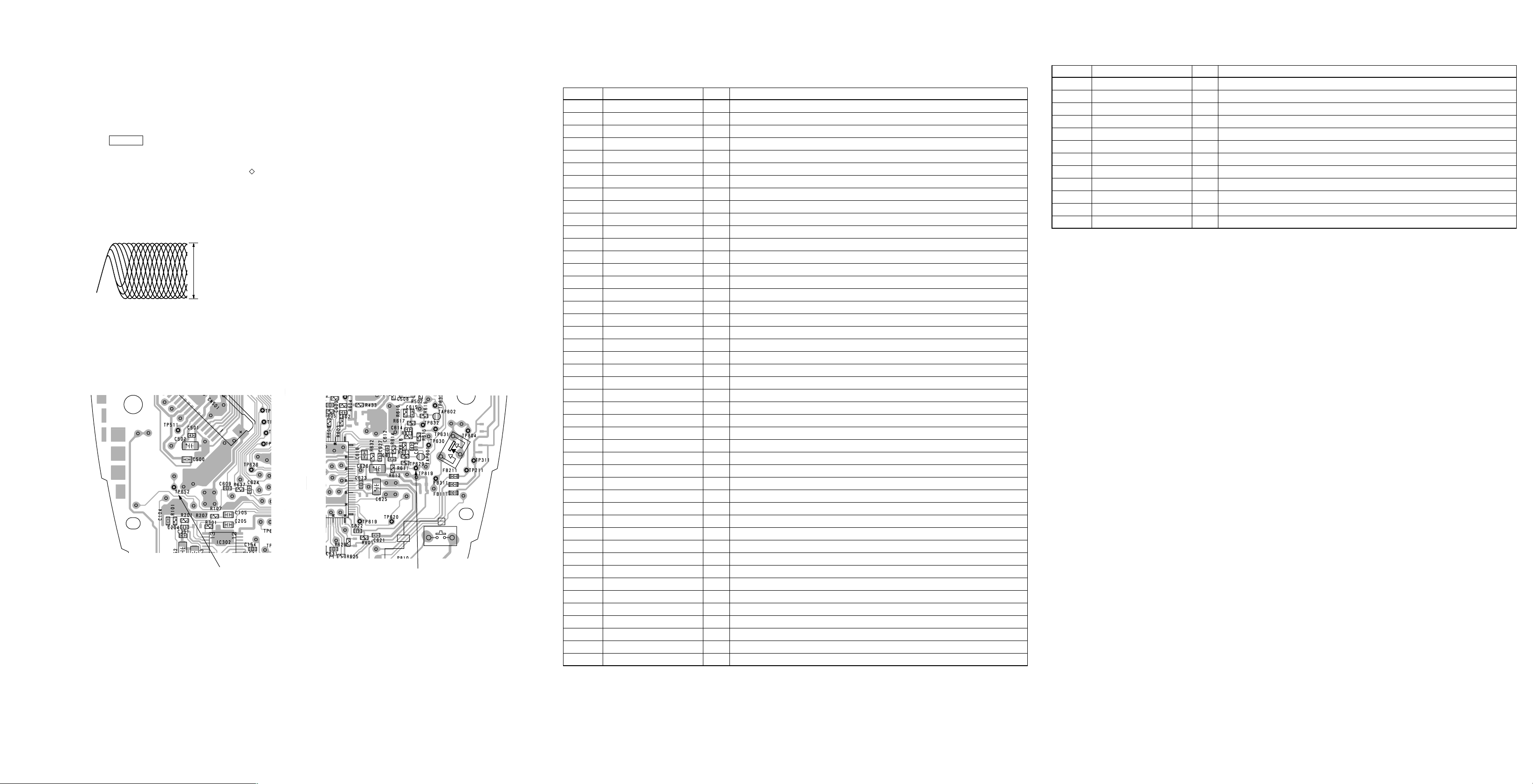
4-1. FOCUS BIAS CHECK
1. Connect the oscilloscope between TP629 (RF) or TP652 (RF)
and GND on main board.
2. Insert the disc (YEDS-18). (Part No. : 3-702-101-01)
3. Press the N > button.
4. Confirm that the oscilloscope waveform is as shown in the
figure below. (eye pattern)
A good eye pattern means that the diamond shape ( ) in the
center of the waveform can be clearly distinguished.
• RF signal reference waveform (eye pattern)
VOLT/DIV : 20 mV (10 : 1 probe in use)
TIME/DIV : 500 nS
RF level :
0.46 - 0.66 Vp-p
When observing the eye pattern, set the oscilloscope for AC range
and raise vertical sensitivity.
Test Points:
– MAIN BOARD – (SIDE A)
TP652
– MAIN BOARD – (SIDE B)
VOL
TP629
S805
S804
5-1. IC PIN DESCRIPTION
• IC801 TMP88CM22F (SYSTEM CONTROLLER)
Pin No. Pin Name I/O Pin Description
1 VSS — Ground
2 RESERVE — Not used (Open)
3 FOK I I Focus OK signal input from digital servo processor (IC601).
4 AGCPWM O O AGC control pulse output
5, 6 RESERVE — Not used (Open)
7 AMUTE O O Analog audio muting ON/OFF signal control signal output (H: Mute ON)
8 RESERVE — Not used (Open)
9 XRST O O Reset signal output to CXD3027R (IC601). (L: Reset)
10 SCK O O Serial data transfer clock signal output to CXD3027R (IC601).
11 MSDT I (SENS) I Serial data input from CXD3027R (IC601).
12 MSDT O O Serial data output to CXD3027R (IC601).
13 WAKEUP O O WAKE-UP control signal output (for system standby reset)
14 AD SEL I Plug-in detection signal input of LINE OUT/OPTICAL OUT jack.
15 AD CHGMNT I Battery charge voltage detection input from power control IC (IC401).
16 RESERVE — Fixed at H.
17 AD BATMNT I Battery voltage detection input
18 AD KEY1 I Key input from switch unit (A/D input)
19 RESERVE — Fixed at H.
20 AD DCINMNT I DC input voltage detection input (A/D input) DC input jack use/no-use detect input
21 WP OPEN I CD door open/close detection input
22 VREFL I Reference voltage (0 V) input for A/D converter.
23 VREFH I Reference voltage (+2 V) input for A/D converter.
24 VDD — Power supply pin (+2 V)
25 SCOR I I Sub code sync detection input from CXD3027R (IC601).
26 GRSCOR I I GRSCOR signal input
27 FG I I FG pulse input
28 BEEP O O Beep sound output to headphone AMP (IC302).
29 – 32 RESERVE — Not used (Open)
33 COMPRESSION I Key input from EPS switch (S804).
34 27/37 — Not used (Open)
35 WFCKI I WFCK input
36 XWRE — Not used (Open)
37 XQOK — Not used (Open)
38 DBB I I MEGA BASS switch (S802) input (L: OFF, H: ON)
39 HOLD I I HOLD switch (S803) input (L: HOLD on, H: HOLD off)
40, 41 RESERVE — Not used (Open)
42 XHGON — Not used (Open)
43 XLAT O O Serial data latch pulse output to D-RAM controller (IC601). (for ESP)
44 XSOE O O Output enable signal output (for ESP)
45 VOLUME IC LATCH O O Not used (Fixed at H)
46 XPOWLT O O Latch output to VCD control IC (IC401).
47 RESERVE — Not used (Open)
48 XAPC OFF O O APC mute signal output (L: mute)
49 SEG15 — Not used. (Open)
50 – 62 SEG14 – 2 O LCD drive segment output
Pin No. Pin Name I/O Pin Description
63 SEG1 — LCD drive segment output (Open)
64 SEG0 O LCD drive segment output
65 – 68 COM3 – 0 O LCD drive common output
69 – 71 V3 – 1 O LCD drive bias output
72, 73 C1, 0 O Capacitor connected terminal of LCD driver for voltage-up.
74 STOP O Stop signal output to VCD control IC. (Connect to ground.)
75 TEST I Test terminal for IC. Fixed at L.
76 XHPSW O — Not used (Open)
77 XLIGHT O — Not used (Open)
78 RESET I I System reset signal input from power control IC (IC401). (L: Reset)
79 XIN I Oscillation input
80 XOUT O Oscillation output (Open)
– 7 – – 8 – – 9 –
D-E200/E201/E206CK/E251
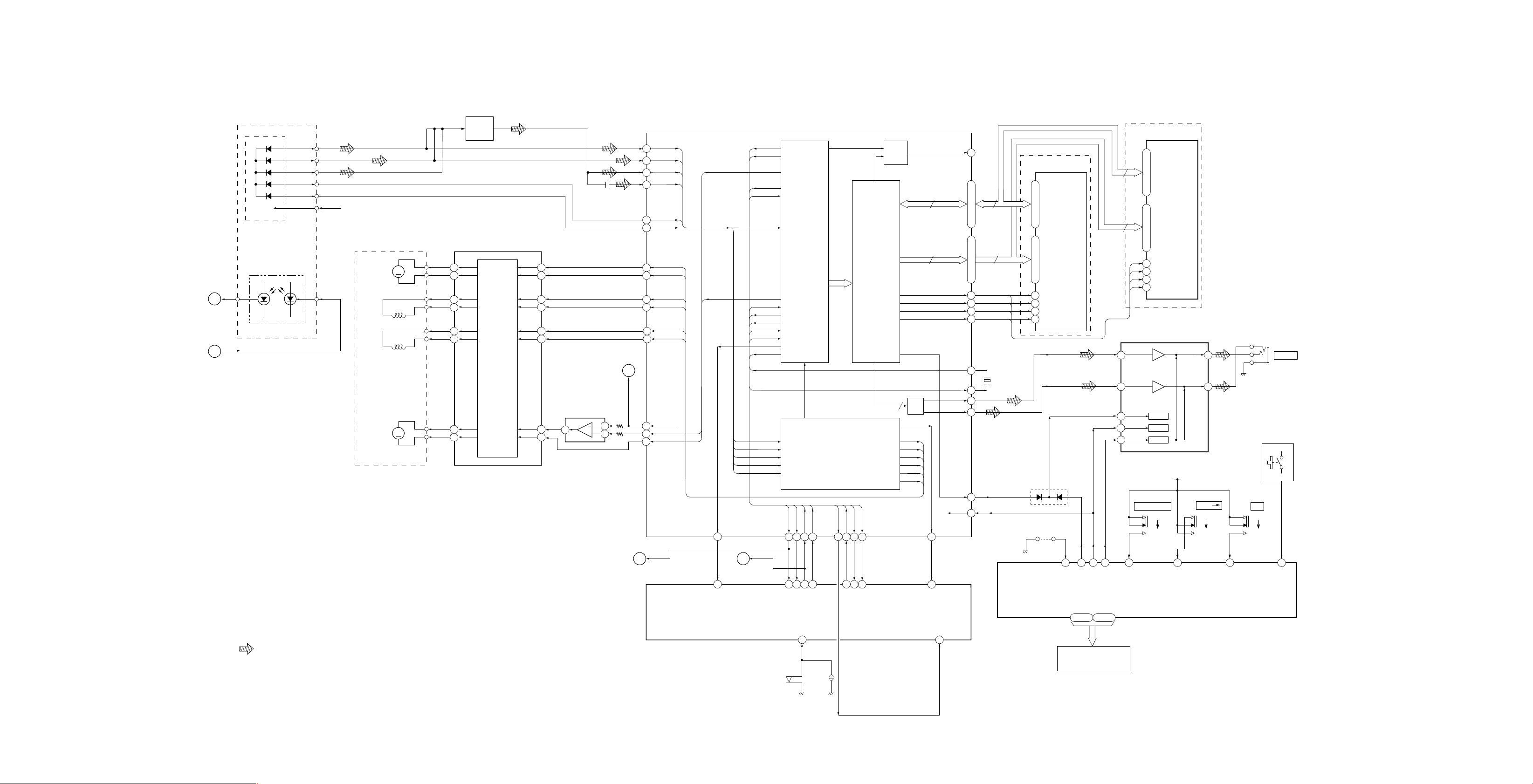
5-2. BLOCK DIAGRAM — CD SECTION —
DETECTOR
A
(Page 13)
B
(Page 13)
PD
LD
A
B
C
E
F
VCC VCC +2.5V
OPTICAL PICK-UP
BLOCK (DAX-11A)
LASER DIODE
PD
A
B
C
E
F
M501
SLED MOTOR
FOCUS
LD
COIL
TRACKING
COIL
M502
SPINDLE
MOTOR
DIGITAL SIGNAL PROCESSOR,
DIGITAL SERVO PROCESSOR,
WFCK
MDS
XTAO
XTAI
RFAC
MDP
XSOE
SENS
R4M
XLAT
CLOK
SCOR
SDTO
RFDC
E
F
B
A
D-RAM CONTROLLER
IC601
SIGNAL
PROCESSOR
BLOCK
SDTO
SENS
CLOK
XLAT
242523
DIGITAL
OUT
MEMORY
CONTROLLER,
BUS BOOST
BLOCK
2
LPF
FOK
FFDR
SERVO
BLOCK
R4M
XSOE
WDCK
WFCK
30 35
2826
83
78
FRDR
TFDR
TRDR
SFDR
SRDR
DOUT
85
D1-D4
4
115 – 118
A0-A10
11 11
1-3, 5-7, 106-109, 111
XRAS
113
XWE
114
XCAS
119
XOE
120
XTAI
93
XTAO
94
LOUT1
97
LOUT2
104
AMUTE
13
XRST
21
FOK
4
X601
16.9MHz
D-E251
D1-D4A0-A10
2, 3, 22, 23
7 - 11, 14 - 19
5
XRAS
4
XWE
21
XCAS
20
XOE
D601
TAP801
(TEST)
D-RAM
IC602
RF AMP
Q501-504
A
62
B
61
RFDC
58
RFAC
71
E
59
F
D
SYNC
60
SFDR
46
SRDR
47
FFDR
50
FRDR
51
TFDR
48
TRDR
49
C176
42
MDP
43
MDS
44
FOCUS/TRACKING COIL DRIVER
SPINDLE/SLED MOTOR DRIVER
IC401 (2/2)
S+
M
S-
F+
F-
T+
T-
FO1
40
RO1
38
FO2
36
34
32
30
RO2
FO3
RO3
CONTROLLER,
PREDRIVER
RI1
RI2
RI3
FI1
41
42
FI2
43
44
FI3
12
13
(Page 13)
BUFFER
IC402
C+
M
C-
FO4
28
RO4
26
PWM
POL
14
4
15
1
+
3
WDCK (GRSCOR)
SCOR
17
10
14
15
19
20
17
4
IN_L
IN_R
MUTE
PW_SW
BEEP
D-E200/E201/E206CK
D-RAM
IC603
D1-D4A0-A9
1, 2, 24, 25
5, 14 - 18
4
XRAS
3
XWE
23
XCAS
22
XOE
HEADPHONE AMP
IC302
MT SW
PW SW
BEEP
VCPU +2V
S802
MEGA BASS
OFF
ON
OUT_L
OUT_R
S803
HOLD
OFF
ON
8
6
S804
J302
PHONES
S805-S810
ESP
OFF
ON
(Page 13)
SDTO
C
SCOR
• SIGNAL PATH
: CD PLAY
04
E
(Page 13)
SCK
SDTO
SDTI
21
SCKO
OPEN
S801
(OPEN)
14 7 9 28 39 18
35114443101225
26
XLATO
XSOEO
TAP802
(OPEN)
WFCKI
SYSTEM CONTROLLER
GRSCORI
IC801 (2/3)
3
FOKI
XINI
79
SYSTEM CONTROLLER
IC801(3/3)
ADSEL
LIQUID CRYSTAL DISPLAY
XRST
AMUTE
SEG14
I
SEG0
50 - 64 65 - 68
PANEL
LCD801
COM3
I
BEEP
COM0
38
DBBI
HOLDI
– 10 – – 11 – – 12 –
33
ADKEY1
COMPRESSION
 Loading...