

Sony Cybershot DCR-SR100,Cybershot DCR-SR90E,Cybershot DCR-SR100E Service Manual
DCR-SR90E/SR100/SR100E
RMT-835
SERVICE MANUAL
Ver. 1.2 2007.04
Revision History
Revision History
How to use
How to use
Acrobat Reader
Acrobat Reader
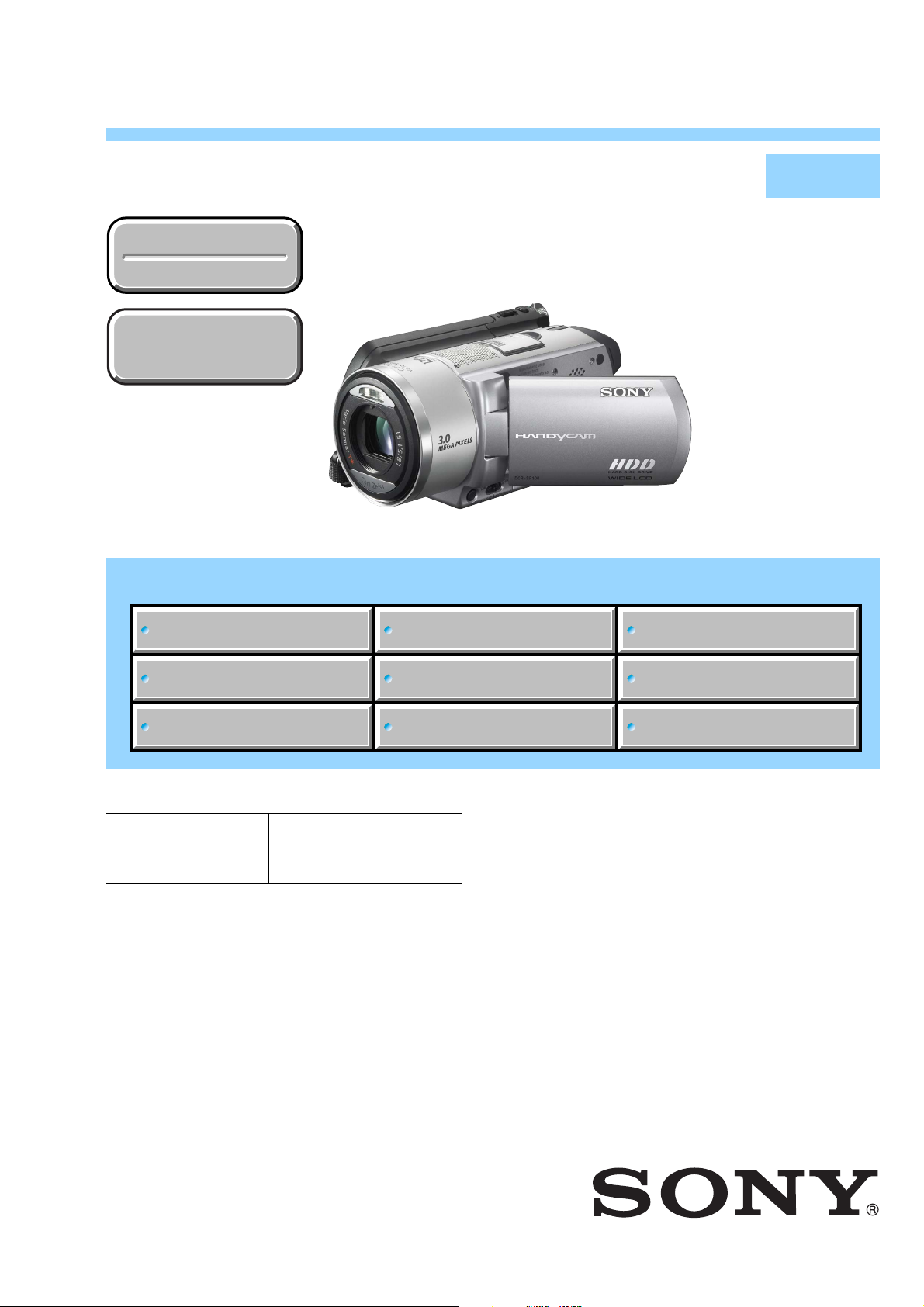
Photo: DCR-SR100
Link
Link
SPECIFICATIONS
DISASSEMBLY
LEVEL 2
US Model
Canadian Model
AEP Model
UK Model
North European Model
E Model
Australian Model
Hong Kong Model
Chinese Model
Korea Model
Tourist Model
Japanese Model
SCHEMATIC DIAGRAMS
MODEL INFORMATION TABLE
SERVICE NOTE
• Precaution on Replacing the VC-449 Board
The components identified by
mark 0 or dotted line with
mark 0 are critical for safety.
Replace only with part number specified.
Les composants identifiés par une
marque 0 sont critiques pour la
sécurité.
Ne les remplacer que par une pièce
portant le numéro spécifié.
BLOCK DIAGRAMS
FRAME SCHEMATIC DIAGRAM
PRINTED WIRING BOARDS
REPAIR PARTS LIST
DIGITAL VIDEO CAMERA RECORDER
DCR-SR90E/SR100/SR100E_L2
9-876-940-31
Sony EMCS Co.
2007D0500-1
© 2007.4
Published by Kohda TEC

These specifications are extracted from instruction
manual of DCR-SR90E/SR100E.
SPECIFICATIONS
ENGLISH JAPANESE
ENGLISH JAPANESE
System
Video compression format
MPEG2/JPEG (Still images)
Hard Disk
30 GB
Audio compression format
Dolby Digital 2/5.1ch
Dolby Digital 5.1 Creator
Video signal
PAL color, CCIR standards
Recording format
Movie
MPEG2-PS
Still image
*1
Exif
Ve r. 2.2
Recording/playback time
HQ:Approx. 440 min
SP:Approx. 650 min
LP: Approx. 1 250 min
Number of recordable movies/still images
Movie: Maximum of 9 999
Still image: Maximum of 9 999
Viewfinder
Electric viewfinder
color
Image device
5.9 mm (1/3 type) CCD (Charge Coupled
Device)
Gross:
Approx. 3 310 000 pixels
Effective (Movie, 4:3):
Approx. 2 050 000 pixels
Effective (Movie, 16:9):
Approx. 2 060 000 pixels
Effective (Still, 4:3):
Approx. 3 050 000 pixels
Effective (Still, 16:9):
Approx. 2 290 000 pixels
Lens
Carl Zeiss Vario-Sonnar T
Filter diameter:30 mm (1 3/16 in.)
Optical:10×, Digital:20×, 120×
F=1.8 - 2.9
Focal length
f=5.1 - 51 mm (7/32 - 2 1/8 in.)
When converted to a 35 mm still camera
For movies:
42.8 - 495 mm (1 11/16 - 19 1/2 in.) (16: 9)
45 - 450 mm (1 13/16 - 17 3/4 in.) (4:3)
For still images:
40.6 - 406 mm (1 5/8 - 16 in.) (16:9 )
37 - 370 mm (1 1/2 - 14 5/8 in.) (4:3)
Color temperature
[AUTO], [ONE PUSH], [INDOOR] (3 200 K),
[OUTDOOR] (5 800 K)
Minimum illumination
5 lx (lux) (F1.8)
0 lx (lux) (in the NightShot function)
*1
“Exif” is a file format for still images, established
by the JEITA (Japan Electronics and Information
Technology Industries Association). Files in this
format can have additional information such as
your camcorder’s setting information at the time
of recording.
*2
In 16:9 mode, the focal length figures are actual
figures resulting from wide angle pixel readout.
•Manufactured under license from Dolby
Laboratories.
Input/Output connectors
DCR-SR90E
Audio/Video output
10-pin connector
Video signal: 1 Vp-p, 75Ω (ohms), unbalanced
Luminance signal: 1 Vp-p, 75Ω (ohms),
unbalanced
Chrominance signal: 0.3Vp-p, 75 Ω (ohms),
unbalanced
Audio signal: 327 mV (at load impedance 47
kΩ (kilohms)), Output impedance with less
than 2.2 kΩ (kilohms)
USB jack
mini-B
REMOTE jack
Stereo mini-minijack (Ø 2.5 mm)
DCR-SR100E
Audio/Video input/output
10 pin connector
Input/Output auto switch
Video signal: 1 Vp-p, 75Ω (ohm s), unbalanced
Luminance signal: 1 Vp-p, 75Ω (ohms),
unbalanced
Chrominance signal: 0.3 Vp-p, 75Ω (ohms),
unbalanced
Audio signal: 327 mV (at load impedance
47 kΩ (kilohms)), Input impedance more than
47 kΩ (kilohms), Output impedance less than
2.2 kΩ (kilohms)
USB jack
mini-B
REMOTE jack
Stereo mini-minijack (Ø 2.5 mm)
LCD screen
Picture
6.9 cm (2.7 type, aspect ratio 16:9)
To tal number of pixels
123 200 (560 × 220)
General
Power requirements
7.2 V (battery pack) 8.4 V (AC Adaptor)
Average power consumption (when using the
*2
battery pack)
During camera recording using LCD
4.1 W
Viewfinder
3.7 W
Operating temperature
0°C to + 40°C (32°F to 104°F)
Storage temperature
-20°C to + 60°C (-4°F to + 140°F)
Dimensions (Approx.)
82 × 69 × 149 mm (3 3/8 × 2 3/4 × 5 7/8 in.)
(w×h×d)
Mass (Approx.)
535 g (1 lb 2 oz) main unit only
615 g (1 lb 5 oz) including the NP-FP60
rechargeable battery pack
Supplied accessories
AC Adaptor (1)
Mains lead (1)
A/V connecting cable (1)
USB cable (1)
Wireless Remote Commander (1)
Rechargeable battery pack
NP-FP60 (1)
CD-ROM “ImageMixer for HDD
Camcorder” (1)
“Camera Operating Guide” (1)
“Computer Application Guide” (1)
See page 5-26.
AC Adap
Power requirements
Current consumption
Power consumption
Output voltage
Operating temperature
Storage temperature
Dimensions (Approx.)
Mass (Approx.)
* See at the label of AC Adaptor for other
tor AC-L200
AC 100 - 240 V, 50/60 Hz
0.35 - 0.18 A
18 W
DC 8.4 V*
0°C to + 40°C (32°F to 104°F)
-20°C to + 60°C (-4°F to + 140°F)
48 × 29 × 81 mm (1 15/16 × 1 3/16 × 3 1/4 in.)
(w×h×d) excluding the projecting parts
170 g (6 oz) excluding the mains lead
specifications.
Rechargeable battery pack
NP-FP60
Maximum outp
DC 8.4 V
Output
DC 7.2 V
Capacity
7.2 wh (1 000 mAh)
Dimensions (Approx.)
31.8 × 33.3 × 45.0 mm
(1 5/16 × 1 5/16 × 1 13/16 in.) (w×h×d)
Mass (Approx.)
80 g (2.9 oz)
Operating temperature
0°C to + 40°C (32°F to 104°F)
Typ e
Li-ion
Design and specifications are subject to change
without notice.
ut voltage
voltage
DCR-SR90E/SR100/SR100E_L2
— 2 —

概略仕様
ENGLISH JAPANESE
ENGLISH JAPANESE
システム
映像圧縮方式
MPEG2/JPEG
ハードディスク
30GB
音声圧縮方式
Dolby Digital2/5.1ch
ドルビーデジタル
記録フォーマット
動画
MPEG2-PS
静止画
Exif Ver.2.2
映像信号
NTSC
再生時間
録画
/
:約
HQ
:約
LP
撮影可能カット数
動画:
静止画:
ファインダー
電子ファインダー:カラー
撮像素子
5.9mm(1/3
総画素数:約
動画有効画素数(
動画有効画素数(
静止画有効画素数(
静止画有効画素数(
レンズ
カールツァイス バリオゾナー
倍(光学)、20倍、
10
フィルター径
値=
F
f(焦点距離):
35mm
動画撮影時
42.8-495
45-450
静止画撮影時
40.6-406mm(16:9
37-370
色温度切り換え
[オート]、[ワンプッシュ]、[屋内](
[屋外](
最低被写体照度
(ルクス)(
11 lx
(ルクス)(
0 lx
*1
(社)電子情報技術産業協会(
された、撮影情報などの付帯情報を追加する
ことができる静止画用のファイルフォーマッ
ト
*2
広角画素読み出しによる実動作値
ドルビーラボラトリーズからの実施権に基づ
•
き製造されています。
(静止画)
*1
カラー、
EIA
分 SP:約
440
分
1 250
枚数
/
個
9 999
枚
9 999
型)
331
30mm
1.8-2.9
5.1-51mm
カメラ換算:
mm(16:9)
mm(4:3)
mm(4:3)
5800K
NightShot
クリエーター搭載
5.1
標準方式
650
固体撮像素子
CCD
万画素
):約
4:3
205
):約
16:9
):約
4:3
):約
16:9
倍(デジタル)
120
*2
)
)
)
F1.8
分
206
305
229
時)
JEITA
万画素
万画素
万画素
万画素
T
)にて制定
3200K
)、
入/出力端子
端子
A/V
ピン特殊コネクター
10
入力
出力自動切り換え
/
USB
映像:
出力
Y
出力
C
音声:
ダンス
Ω以下
k
端子
mini-B
1 Vp-p、75
327mV(47 k
47 k
Ω不平衡
1Vp-p、75
0.286Vp-p、75
Ω不平衡
Ω不平衡
Ω負荷時)、入力インピー
Ω以上、出力インピーダンス
REMOTE
ステレオミニミニジャック(リモート)端子
(
ø2.5mm
)
液晶画面
画面サイズ
6.9cm(2.7
総ドット数
123 200
型アスペクト比
ドット 横
560
×縦
16:9
220
電源部、その他
電源電圧
バッテリー端子入力
端子入力
DC
消費電力(バッテリー使用時)
液晶画面使用時:
ファインダー使用時:
動作温度
℃〜
0
+40
保存温度
℃〜
−
20
+60
外形寸法
82×69×149mm
×高さ×奥行き)
本体質量
付属品
(本体のみ)
約
535g
約
(バッテリーパックを含む)
615g
AC
アダプター
電源コード
AV
接続ケーブル
USB
ケーブル
ワイヤレスリモコン
リチャージャブルバッテリーパック
NP-FP60
(1)
CD-ROM
「ImageMixerforHDD
Camcorder」(1)
取扱説明書
取扱説明書「パソコン編」
保証書
(1)
7.2V
8.4V
4.3W
3.9W
℃
℃
(最大突起部を除く)(幅
(1)
(1)
(1)
(1)
(1)
(1)
(1)
)
2.2
アダプター
AC
電源
AC-L200
AC100〜240V、50/60Hz
消費電力
18W
定格出力
DC8.4V*
動作温度
℃〜
0
保存温度
−
外形寸法
約
(幅×高さ×奥行き)
質量
約
その他の仕様についてはACアダプターのラ
*
ベルをご覧ください。
℃
+40
℃〜
+60
℃
20
48×29×81mm
(本体のみ)
170g
(最大突起部をのぞく)
リチャージャブルバッテリーパック
NP-FP60
最大電圧
DC8.4V
公称電圧
DC7.2V
容量
7.2wh(1 000mAh
最大外形寸法
約
31.8×33.3×45.0mm
(幅×高さ×奥行き)
質量
約
80g
使用温度
℃〜
0
+40
使用電池
Li-ion
)
℃
DCR-SR90E/SR100/SR100E_L2
— 3 —

Model information table
Model DCR-SR90E DCR-SR100 DCR-SR100E
Destination AEP, UK US, CND, E, KR, JE, J NE, E, AUS, HK, CH, JE
Color system PAL NTSC PAL
A/V line input × aa
CAM → PC aaa
Data
copy
PC → CAM × aa
•Abbreviation
AR : Argentine model
AUS: Australian model
BR : Brazilian model
CH : Chinese model
CND : Canadian model
EE : East European model
HK : Hong Kong model
J: Japanese model
JE : Tourist model
KR : Korea model
MX : Mexican model
NE : North European model
DCR-SR90E/SR100/SR100E_L2
— 4 —
ENGLISH JAPANESE
ENGLISH JAPANESE
Danger of explosion if battery is incorrectly replaced.
CAUTION
Replace only with the same or equivalent type.
SAFETY-RELATED COMPONENT WARNING!!
COMPONENTS IDENTIFIED BY MARK 0 OR DO TTED LINE WITH
MARK 0 ON THE SCHEMATIC DIAGRAMS AND IN THE PARTS
LIST ARE CRITICAL TO SAFE OPERATION. REPLACE THESE
COMPONENTS WITH SONY PARTS WHOSE PART NUMBERS
APPEAR AS SHOWN IN THIS MANUAL OR IN SUPPLEMENTS
PUBLISHED BY SONY.
SAFETY CHECK-OUT
After correcting the original service problem, perform the following
safety checks before releasing the set to the customer.
1. Check the area of your repair for unsoldered or poorly-soldered
connections. Check the entire board surface for solder splashes
and bridges.
2. Check the interboard wiring to ensure that no wires are
"pinched" or contact high-wattage resistors.
3. Look for unauthorized replacement parts, particularly
transistors, that were installed during a previous repair . Point
them out to the customer and recommend their replacement.
4. Look for parts which, through functioning, show obvious signs
of deterioration. Point them out to the customer and
recommend their replacement.
5. Check the B+ voltage to see it is at the values specified.
6. Flexible Circuit Board Repairing
•Keep the temperature of the soldering iron around 270˚C
during repairing.
• Do not touch the soldering iron on the same conductor of the
circuit board (within 3 times).
• Be careful not to apply force on the conductor when soldering
or unsoldering.
ATTENTION AU COMPOSANT AYANT RAPPORT
À LA SÉCURITÉ!
LES COMPOSANTS IDENTIFÉS PAR UNE MARQUE 0 SUR LES
DIAGRAMMES SCHÉMA TIQ UES ET LA LISTE DES PIÈCES SONT
CRITIQUES POUR LA SÉCURITÉ DE FONCTIONNEMENT. NE
REMPLACER CES COMPOSANTS QUE PAR DES PIÈSES SONY
DONT LES NUMÉROS SONT DONNÉS DANS CE MANUEL OU
DANS LES SUPPÉMENTS PUBLIÉS PAR SONY.
Unleaded solder
Boards requiring use of unleaded solder are printed with the leadfree mark (LF) indicating the solder contains no lead.
(Caution: Some printed circuit boards may not come printed with
the lead free mark due to their particular size.)
: LEAD FREE MARK
Unleaded solder has the following characteristics.
• Unleaded solder melts at a temperature about 40°C higher than
ordinary solder.
Ordinary soldering irons can be used but the iron tip has to be
applied to the solder joint for a slightly longer time.
Soldering irons using a temperature regulator should be set to
about 350°C.
Caution: The printed pattern (copper foil) may peel away if the
heated tip is applied for too long, so be careful!
• Strong viscosity
Unleaded solder is more viscous (sticky, less prone to flow) than
ordinary solder so use caution not to let solder bridges occur such
as on IC pins, etc.
•Usable with ordinary solder
It is best to use only unleaded solder but unleaded solder may
also be added to ordinary solder.
DCR-SR90E/SR100/SR100E_L2
— 5 —
ENGLISH JAPANESE
ENGLISH JAPANESE
電池の交換は,正しく行わないと破裂する恐れがあり
注意
ます。電池を交換する場合には必ず同じ型名の電池
又は同等品と交換してください。
サービス,点検時には次のことにご注意下さい。
1. 注意事項をお守りください。
サービスのとき特に注意を要する個所については,
キャビネット,シャーシ,部品などにラベルや捺印で
注意事項を表示しています。これらの注意書き及び取
扱説明書等の注意事項を必ずお守り下さい。
2. 指定部品のご使用を
セットの部品は難燃性や耐電圧など安全上の特性を
持ったものとなっています。従って交換部品は,使用
されていたものと同じ特性の部品を使用して下さい。
特に回路図,部品表に0印で指定されている安全上重要
な部品は必ず指定のものをご使用下さい。
3. 部品の取付けや配線の引きまわしはもとどおりに
安全上,チューブやテープなどの絶縁材料を使用した
り,プリント基板から浮かして取付けた部品がありま
す。また内部配線は引きまわしやクランパによって発
熱部品や高圧部品に接近しないよう配慮されています
ので,これらは必ずもとどおりにして下さい。
4. サービス後は安全点検を
サービスのために取外したネジ,部品,配線がもとど
おりになっているか,またサービスした個所の周辺を
劣化させてしまったところがないかなどを点検し,安
全性が確保されていることを確認して下さい。
5. チップ部品交換時の注意
• 取外した部品は再使用しないで下さい。
• タンタルコンデンサのマイナス側は熱に弱いため交
換時は注意して下さい。
6. フレキシブルプリント基板の取扱いについて
• コテ先温度を270℃前後にして行なって下さい。
• 同一パターンに何度もコテ先を当てないで下さい。
(3回以内)
• パターンに力が加わらないよう注意して下さい。
7. 無鉛半田について
無鉛半田を使用している基板には,無鉛(LeadFree)を
意味するレッドフリーマークがプリントされています。
(注意:基板サイズによっては,無鉛半田を使用して
いてもレッドフリーマークがプリントされて
いないものがあります)
:レッドフリーマーク
無鉛半田には,以下の特性があります。
• 融点が従来の半田よりも約40℃高い。
従来の半田こてをそのまま使用することは可能です
が,少し長めにこてを当てる必要があります。
温度調節機能のついた半田こてを使用する場合,約
350℃に設定して下さい。
注意: 半田こてを長く当てすぎると,基板のパター
ン(銅箔)がはがれてしまうことがあります
ので,注意して下さい。
• 粘性が強い
従来の半田よりも粘性が強いため,IC端子などが半田
ブリッジしないように注意して下さい。
• 従来の半田と混ぜて使用可能
無鉛半田には無鉛半田を追加するのが最適ですが,
従来の半田を追加しても構いません。
DCR-SR90E/SR100/SR100E_L2
— 6 —

TABLE OF CONTENTS
Section Title Page
1. SERVICE NOTE
1-1. Power Supply During Repairs·········································1-1
1-2. Setting The “Forced Power On” Mode····························1-1
1-3. Self-diagnosis Function ···················································1-2
1-4. Process After Fixing Flash Error ·····································1-4
1-5. Precaution on Replacing The VC-449 Board ··················1-4
2. DISASSEMBLY
2-1. Disassembly·····································································2-1
3. BLOCK DIAGRAMS
3-1. Overall Block Diagram (1/5)··········································· 3-1
3-2. Overall Block Diagram (2/5)··········································· 3-2
3-3. Overall Block Diagram (3/5)··········································· 3-3
3-4. Overall Block Diagram (4/5)··········································· 3-4
3-5. Overall Block Diagram (5/5)··········································· 3-5
3-6. Power Block Diagram (1/3)············································· 3-6
3-7. Power Block Diagram (2/3)············································· 3-7
3-8. Power Block Diagram (3/3)············································· 3-8
4. PRINTED WIRING BOARDS AND
SCHEMATIC DIAGRAMS
4-1. Frame Schematic Diagram ··············································4-1
4-2. Schematic Diagrams························································4-3
4-3. Printed Wiring Boards ···················································4-33
4-4. Mounted Parts Location ················································4-52
5. REPAIR PARTS LIST
5-1. Exploded V iews·······························································5-2
5-2. Electrical Parts List ······················································· 5-10
DCR-SR90E/SR100/SR100E_L2
— 7 —

ENGLISH JAPANESE
1. SERVICE NOTE
ENGLISH JAPANESE
1-1. POWER SUPPLY DURING REPAIRS
In this unit, about 10 seconds after power is supplied to the battery terminal using the regulated power supply (8.4V), the power is shut off so
that the unit cannot operate.
These following method is available to prevent this.
Method:
Use the AC power adaptor (AC-L200).
1-2. SETTING THE “FORCED POWER ON” MODE
It is possible to turn on power by adjustment remote commander (RM-95 or NEW LANC JIG).
Operate the camcorder using the adjustment remote commander.
1-2-1. Setting the “Forced Movie Power ON” Mode
1) Select page: 0, address: 01, and set data:01.
2) Select page: A, address: 10, set data:01 and press the “PAUSE (Write)” button of the adjustment remote commander.
1-2-2. Setting the “Forced Play/Edit Power ON” Mode
1) Select page: 0, address: 01, and set data:01.
2) Select page: A, address: 10, set data:02 and press the “PAUSE (Write)” button of the adjustment remote commander.
1-2-3. Exiting the “Forced Power ON” Mode
1) Select page: 0, address: 01, and set data:01.
2) Select page: A, address: 10, set data:00 and press the “PAUSE (Write)” button of the adjustment remote commander.
3) Select page: 0, address: 01, and set data: 00.
DCR-SR90E/SR100/SR100E_L2
1-1
1-3. SELF-DIAGNOSIS FUNCTION
ENGLISH JAPANESE
ENGLISH JAPANESE
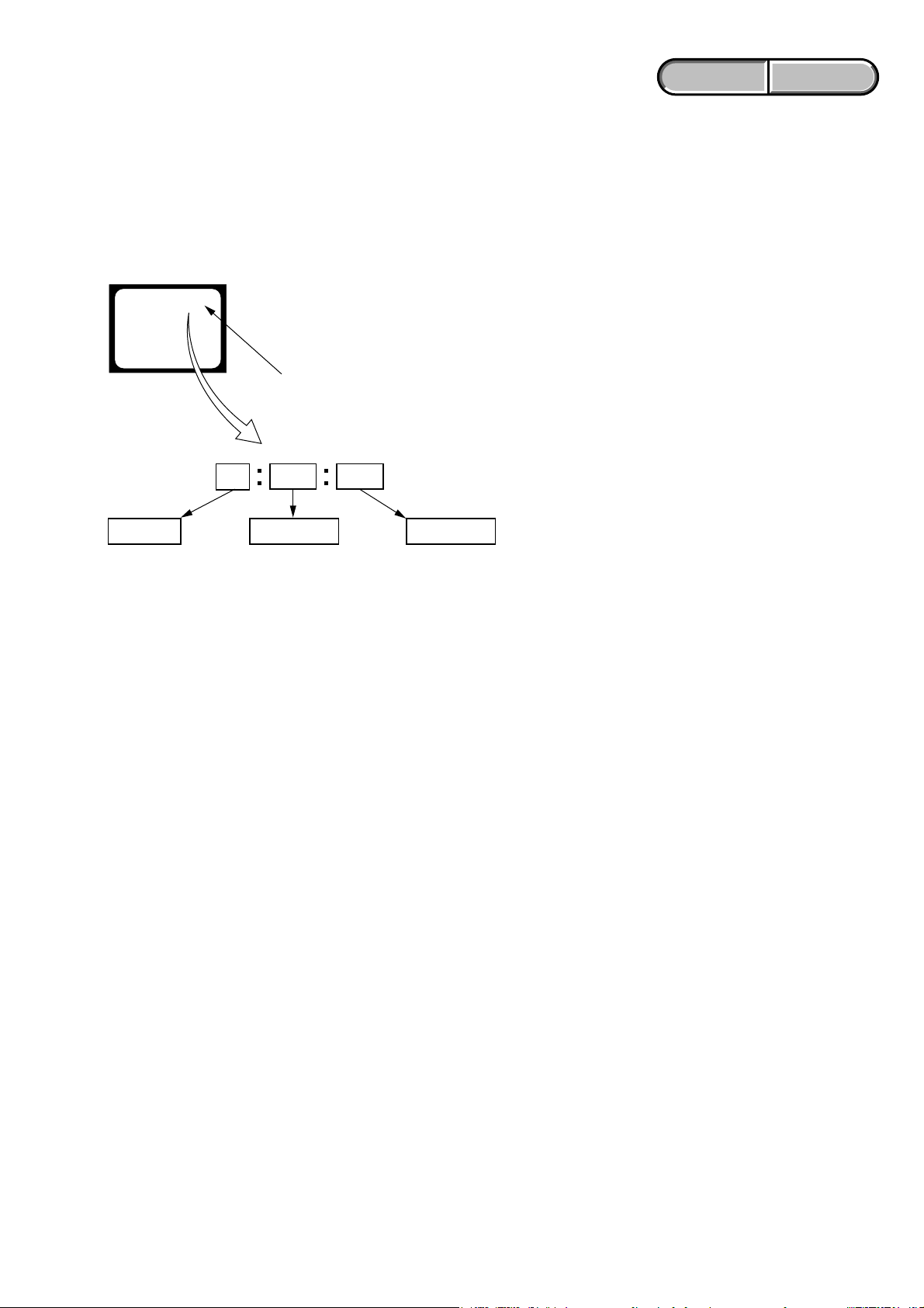
1-3-1. Self-diagnosis Function
When problems occur while the unit is operating, the self-diagnosis
function starts working, and displays on the viewfinder or LCD
screen what to do. This function consists of two display; selfdiagnosis display and service mode display.
Details of the self-diagnosis functions are provided in the Instruction
manual.
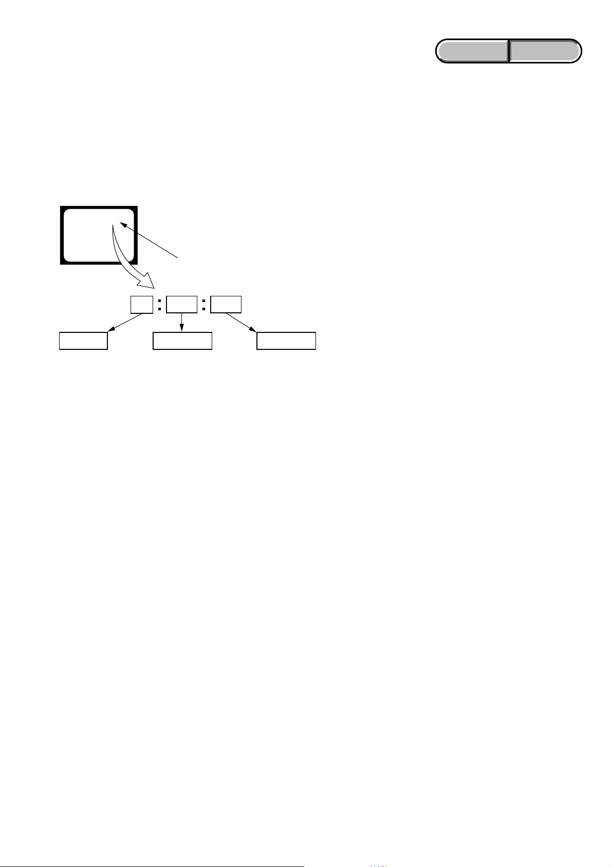
Viewfinder or LCD screen
C : 3 1 : 1 1
Blinks at 3.2Hz
1 1
Refer to “1-3-3. Self-diagnosis Code Table”.
Repaired by:
C : Corrected by customer
H : Corrected by dealer
E : Corrected by service
engineer
3 1C
Block
Indicates the appropriate
step to be taken.
E.g.
31 ....Reload the tape.
32 ....Turn o n power again.
1-3-2. Self-diagnosis Display
When problems occur while the unit is operating, the counter of the
viewfinder or LCD screen shows a 4-digit display consisting of an
alphabet and numbers, which blinks at 3.2 Hz. This 5-character
display indicates the “repaired by:”, “block” in which the problem
occurred, and “detailed code” of the problem.
Detailed Code
DCR-SR90E/SR100/SR100E_L2
1-2
1-3-3. Self-diagnosis Code Table
Self-diagnosis Code
ENGLISH JAPANESE
ENGLISH JAPANESE
Block
Function
Repaired by:
C
04
C
13
C
13
C
21
C
32
E
20
E
31
E
40
E
40
E
61
E
61
E
61
E
62
E
62
E
91
E
94
E
94
Note 1: Refer to “ 12-2. Record of Self-diagnosis check” of “2-5. SERVICE MODE”, ADJ (9-876-940-51).
Note 2: After repair, be sure to perform “1-4. PROCESS AFTER FIXING FLASH ERROR”.
Detailed
Code
00
00
02
00
50
00
00
00
01
00
10
11
00
01
01
00
01
-
Symptom/State
Non-standard battery is used.
Faulty disc is used.
Disc access error
Condensation.
Codec IC dose not return any reply
EEPROM data are rewritten.
Drive fault
Codec IC fault
Audio Codec IC fault
Difficult to adjust focus
(Cannot initialize focus.)
Zoom operations fault
(Cannot initialize zoom lens.)
The abnormalities in initialization of
the focus lens and the abnormalities in
initialization of the zoom lens occurred
simultaneously.
Handshake correction function does not
work well. (With PITCH angular
velocity sensor output stopped.)
Handshake correction function does not
work well. (With YAW angular velocity
sensor output stopped.)
Abnormality when flash is being charged.
Fault of writing to or erasing the
flashmemory
Fault of writing to or erasing EEPROM
Use the InfoLITHIUM battery.
Remove the power source. Reconnect it again and operate your
camcorder again
Remove the power source. Reconnect it again and operate your
camcorder again
Remove the disc, and insert it again after one hour.
Remove the power source. Reconnect it again and operate your
camcorder again
Make EEPROM data correct value. (Note 1)
Inspect or replacement of the hand disc drive
Inspect or replacement of the codec IC (IC2301on the VC-449
board) peripheral circuits
Inspect or replacement of the Audio Codec IC (IC2301 on the
VC-449 board) peripheral circuits
Inspect the lens block focus MR sensor (pin ql, wa of CN1701
on the VC-449 board) when focusing is performed when the
focus buttons of the touch panel are pressed in the focus manual
mode, and the focus motor drive circuit (IC1701 on the VC-449
board) when the focusing is not performed.
Inspect the lens block zoom MR sensor (pin ws, wf of CN1701
on the VC-449 board) when zooming is performed when the
zoom lever is operated, and the zoom motor drive circuit
(IC1701 on the VC-449 board) when zooming is not performed.
Check whether the flexible board of the lens is broken, and
check whether it is inserted imperfectly. If there is no problem in
the flexible board, inspect the focus/zoom motor drive circuit
(IC1701 on the VC-449 board).
Inspect PITCH angular velocity sensors (SE7104 on the IR-057
board) peripheral circuits.
Inspect YAW angular velocity sensors (SE7103 on the IR-057
board) peripheral circuits.
Checking of flash unit or replacement of flash unit. (Note 2)
Inspect the flash memory (IC2401 on the VC-449 board). (Note 1)
Inspect the EEPROM (IC2602 on the VC-449 board). (Note 1)
Correction
DCR-SR90E/SR100/SR100E_L2
1-3
ENGLISH JAPANESE
ENGLISH JAPANESE
1-4. PROCESS AFTER FIXING FLASH ERROR
When “FLASH error” (Self-diagnosis Code E:91:**) occurs, to prevent an y abnormal situation caused by high v oltage, setting of the flash is
changed automatically to disabling charge and flash setting.
After fixing, this setting needs to be deactivated. Connect the adjustment remote commander and perform the following process.
Order Page Address Data Procedure
17 0175
27 00 01 Press PAUSE button.
37 02 Check the data changes to “01”.
1-5. PRECAUTION ON REPLACING THE VC-449 BOARD
Exif Model Data Check
When you replace to the repairing board, the written data of repairing board also might be changed to original setting.
When the data has changed because of board replaceing etc, check the data setting (Exif Model Data) is right. If not, rewrite to the right value.
Exif Model Data
Page
A
A
A
A
Address
B6
B7
B8
B9
DCR-SR100
31
30
30
00
Data
DCR-SR90E
39
30
45
00
DCR-SR100E
31
30
30
45
Writing Method:
1) Select page: 0, address: 01, and set data: 01.
2) Select page: A, address: B6 to B9, and set the Exif Model Data.
Note: To write in the non-volatile memory (EEPROM), press the PAUSE (Write) button each time to set the data.
3) Select page: 0, address: 01, and set data: 00.
DCR-SR90E/SR100/SR100E_L2
1-4

ENGLISH JAPANESE
1. SERVICE NOTE
ENGLISH JAPANESE
1-1. 修理時の電源供給について
本機では,安定化電源(8.4Vdc)からバッテリ端子に電源を供給した場合,約10秒後にシャットオフし,動作しなくなります。
これを避けるため,下記の方法を用いてください。
方法:
DC入力端子を使用する。(ACアダプタ(AC-L200など)を使用する。)
1-2. 強制電源ONモードの設定
調整リモコン(RM-95またはNEWLANCJIG)を使用して,電源を入れることが出来ます。
カムコーダの操作は調整リモコンで行えます。
1-2-1. 強制Movie電源ONモードの設定
1) ページ:0,アドレス:01にデータ:01をセット。
2) ページ:A,アドレス:10にデータ:01をセットしPAUSE(Write)ボタンを押す。
1-2-2. 強制Play/Edit電源ONモードの設定
1) ページ:0,アドレス:01にデータ:01をセット。
2) ページ:A,アドレス:10にデータ:02をセットしPAUSE(Write)ボタンを押す。
1-2-3. 強制電源ONモードの解除
1) ページ:0,アドレス:01にデータ:01をセット。
2) ページ:A,アドレス:10にデータ:00をセットしPAUSE(Write)ボタンを押す。
3) ページ:0,アドレス:01にデータ:00をセット。
DCR-SR90E/SR100/SR100E_L2
1-5
1-3. 自己診断機能
1-3-1.自己診断機能について
本機の動作に不具合が生じたとき,自己診断機能が働き,
ビューファインダまたはLC D 画面に,どう処置したらよい
か判断できる表示を行います。「自己診断表示」と「サービス
モード表示」の2つの表示があります。自己診断機能につい
ては取扱説明書にも掲載されています。
ビューファインダまたはLCD画面
C : 3 1 : 1 1
3.2Hz点滅
ENGLISH JAPANESE
ENGLISH JAPANESE
1-3-2.自己診断表示
本機の動作に不具合が生じたとき,ビューファインダまたは
LCD画面のカウンタ表示部分がアルファベットと数字の4桁
表示になり,3.2Hzで点滅します。この5文字の表示によっ
て対応者分類および不具合の生じたブロックの分類,不具合
の詳細コードを示します。
対応者分類
C :お客さま自身で対応
H:販売店で対応
E :サービスエンジニア
で対応
3 1C
ブロック分類
対応方法の違いにより分類
例 31・・・テープを入れ直す
32・・・電源を入れ直す
1 1
詳細コード
「1-3-3.自己診断コード表」
を参照
DCR-SR90E/SR100/SR100E_L2
1-6

1-3-3.自己診断コード表
自己診断コード
対
応
者
C
C
C
C
C
E
E
E
E
E
E
E
E
E
E
E
E
ブロック
機能
04
13
13
21
32
20
31
40
40
61
61
61
62
62
91
94
94
詳細
コード
00
00
02
00
50
00
00
00
01
00
10
11
00
01
01
00
01
症状/状態
標準以外のバッテリを使用している
ディスク不良
ディスクアクセスエラー
結露している
CodecIC応答せず
EEPROMが書き換えられている
ドライブ不良
CodecIC不良
オーディオCodecIC不良
フォーカスが合いにくい
(フォーカスの初期化ができない)
ズーム動作の異常(ズームレンズの
初期化ができない)
フォーカス,ズーム異常
手振れ補正が効きにくい(PITCH
角速度センサ出力張り付き)
手振れ補正が効きにくい(YAW角
速度センサ出力張り付き)
フラッシュの充電異常
フラッシュメモリの書込み/消去動
作不良
EEPROMの書込み/消去動作不良
ENGLISH JAPANESE
ENGLISH JAPANESE
対応/方法
インフォリチウムバッテリを使用する。
電源を外し,再度入れ直してから操作する。
電源を外し,再度入れ直してから操作する。
ディスクを取り出し,約1時間後にもう一度入れ直す。
電源を外し,再度入れ直してから操作する。
EEPROMのデータを元の値に戻す(注1)
ハードディスクドライブを点検または交換する。
CodecIC(VC-449基板IC2301)周辺回路を点検または
交換する。
オーディオCodecIC(VC-449基板IC2301)周辺回路を
点検または交換する。
タッチパネルでフォーカス操作をしたときにフォーカス動
作をすれば,レンズブロックのフォーカスMRセンサ
(VC-449基板CN1701ql,waピン)を点検する。フォー
カス動作をしなければフォーカスモータ駆動回路(VC449基板IC1701)を点検する。
ズームレバーを操作したときにズーム動作をすれば,レン
ズブロックのズームMRセンサ(VC-449基板CN1701
ws,wfピン)を点検する。ズーム動作をしなければズーム
モータ駆動回路(VC-449基板IC1701)を点検する。
フレキ切れ,半差し等の点検を行う。問題がない場合は
フォーカス/ズームモータ駆動IC(VC-449基板IC1701)
周辺回路を点検する。
PITCH角速度センサ(IR-057基板SE7104)周辺回路を点
検する。
YAW角速度センサ(IR-057基板SE7103)周辺回路を点
検する。
フラッシュユニットの点検または交換をする。(注2)
フラッシュメモリ(VC-449基板IC2401)を点検する。
(注1)
EEPROM(VC-449基板IC2602)を点検する。(注1)
注1: 調整編(9-876-940-51)「2-5.SERVICEMODE」の「12-2.RecordofSelf-diagnosischeck」を参照してください。
注2: 修理後は,必ず「1-4.フラッシュ異常修理後の処置」を行ってください。
DCR-SR90E/SR100/SR100E_L2
1-7
ENGLISH JAPANESE
ENGLISH JAPANESE
1-4. フラッシュ異常修理後の処置
フラッシュエラー(自己診断コードE:91:**)発生時は、高電圧による異常を防止するために自動的にフラッシュ充電・
発光禁止の設定になります。修理後は、この設定を解除する必要があります。調整用リモコンを接続し、下記の処置を行っ
てください。
順序 ページ アドレス データ 作業内容
17 0175
27 00 01 PAUSEボタンを押す
37 02 データが“01”になることを確認
1-5. VC-449基板交換時の注意
Exif機種データ確認
補修用基板と交換する時,補修用基板に書かれているデータは元の設定と違っている場合があります。
基板交換などでデータが変更された場合は,Exif機種データが正しいか確認し,違っている場合は正しい値に書き換えて下
さい。
Exif機種データ
ページ アドレス
AB6 31
AB7 30
AB8 30
AB9 00
データ
DCR-SR100
書き換え方法:
1) ページ:0,アドレス:01にデータ:01をセットする。
2) ページ:A,アドレス:B6〜B9にExif機種データをセットする。
注: 不揮発性メモリ(EEPROM)に書き込むため,データをセットする度にPAUSE(Write)ボタンを押してください。
3) ページ:0,アドレス:01にデータ:00をセットする。
DCR-SR90E/SR100/SR100E_L2
1-8E
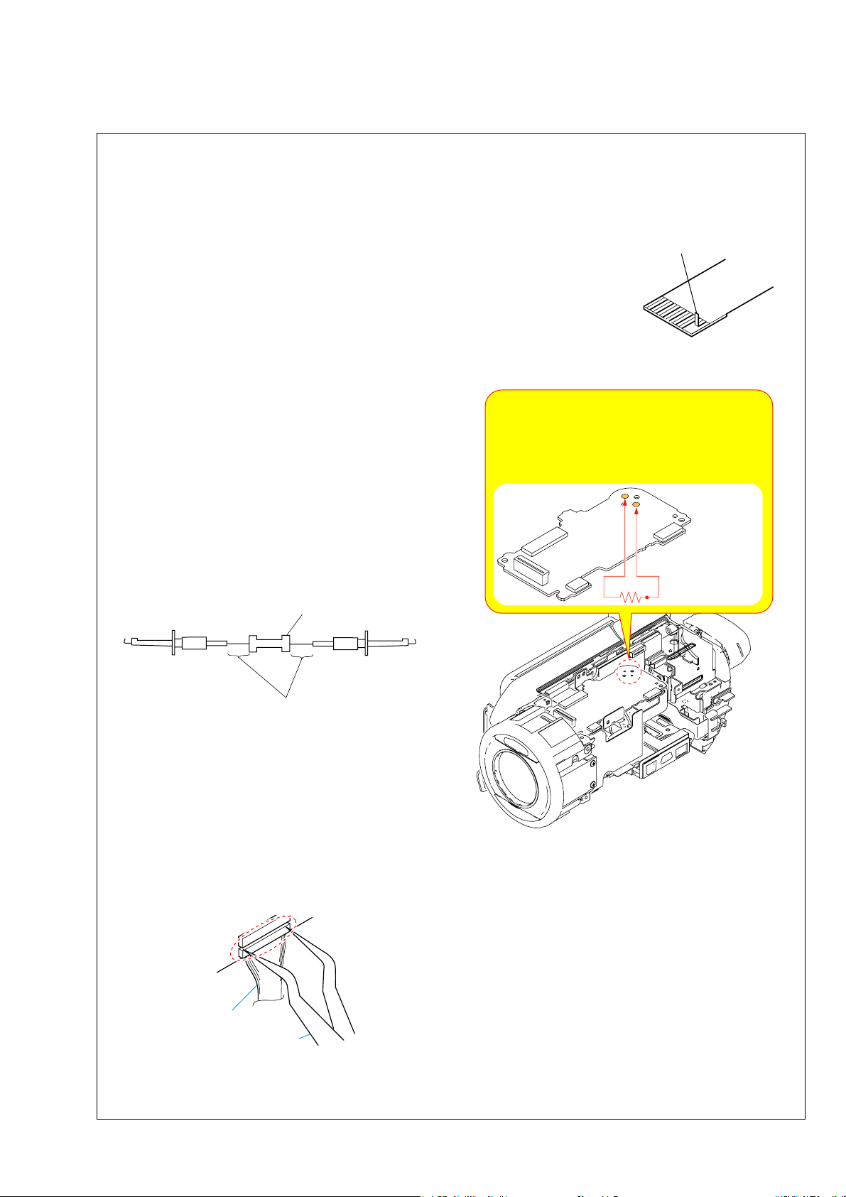
NOTE FOR REPAIR
Note: High-voltage cautions
Discharging the Capacitor
Short-circuit between the two points
with the short jig about 10 seconds.
R:1 kΩ/1 W
(Part code:
1-215-869-11)
2. DISASSEMBLY
• Make sure that the flat cable and flexible board are not cracked of bent at the terminal.
Do not insert the cable insufficiently nor crookedly.
• When remove a connector, dont’ pull at wire of connector. It is possible that a wire is snapped.
• When installing a connector, dont’ press down at wire of connector.
It is possible that a wire is snapped.
Cut and remove the part of gilt
which comes off at the point.
(Be careful or some
pieces of gilt may be left inside)
DISCHARGING OF THE MA-444 BOARD’S CHARGING CAPACITOR (C5306)
The charging capacitor (C5306) of the MA-444 board is charged
up to the maximum 330 V potential.
There is a danger of electric shock by this high voltage when the
capacitor is handled by hand. The electric shock is caused by
the charged voltage which is kept without discharging when the
main power of the unit is simply turned off. Therefore, the
remaining voltage must be discharged as described below.
Preparing the Short Jig
To preparing the short jig, a small clip is attached to each end of
a resistor of 1 kΩ /1 W (1-215-869-11).
Wrap insulating tape fully around the leads of the resistor to
prevent electrical shock.
NOTE FOR DISCONNECTING THE HARNESS (CD-122)
Harness (CD-122)
1 kΩ/1 W
Wrap insulating tape.
When disconnecting the harness (CD-122), do not pull the harness
part but pull off the connector body with tweezers etc.
Tweezers etc.
DCR-SR90E/SR100/SR100E_L2
2-1
HELP
EXPLODED VIEW
HELP
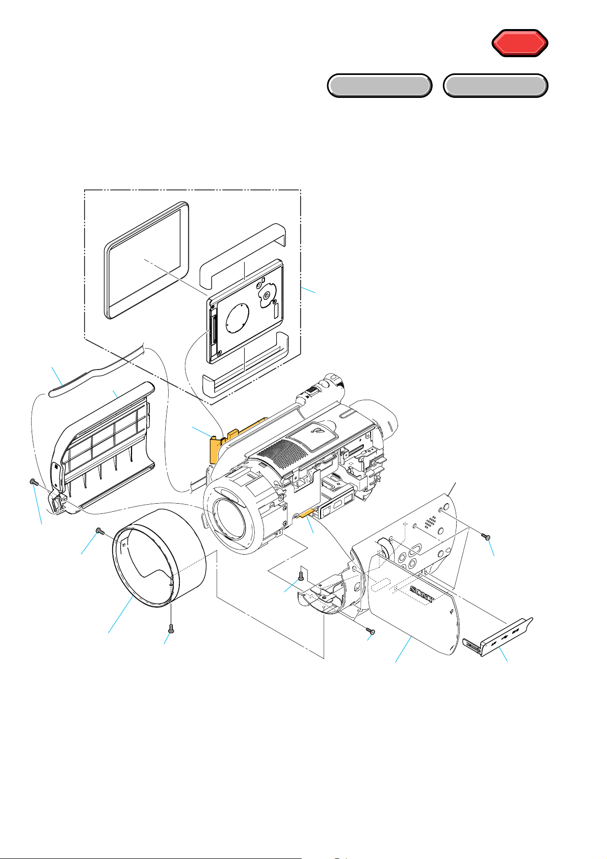
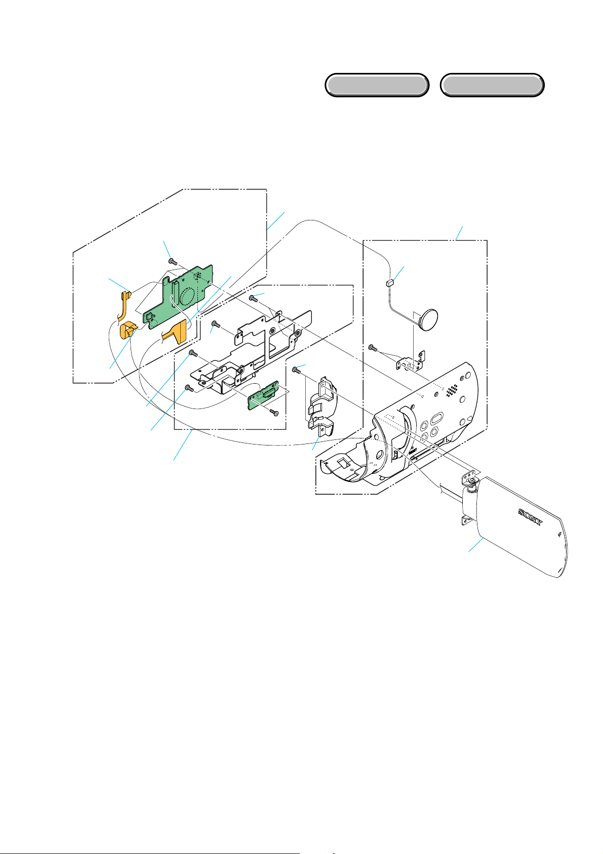
2-1. DISASSEMBLY
2-1-1. OVERALL ASSEMBLY-1
Follow the disassembly in the numerical order given.
1 Lens ring (1-1 to 1-2)
2 HDD (2-1 to 2-4)
3 Cabinet (R) block (3-1 to 3-6)
2-1
HARDWARE LIST
2 HDD
2-2 (#10)
1-1 (#10)
1 Lens ring
2-3
2-4
1-2 (#10)
3-1 (#10)
3-6
3-2 (#10)
3 Cabinet (R) block
3-3
(Open the panel block)
3-5 (#10)
3-4
DCR-SR90E/SR100/SR100E_L2
2-2
2-1-2. OVERALL ASSEMBLY-2
EXPLODED VIEW
Follow the disassembly in the numerical order given.
1 Panel (top) block (1-1 to 1-7)
2 EVF/BT panel block (2-1 to 2-7)
3 Lens block (3-1 to 3-7)
HARDWARE LIST
1-6 (#10)
3-6 (#10)
1-4 (#10)
1-2
3-3 (#14)
1-5 (#14)
1-3 (#14)
3-2
1-1
1 Panel (top) block
2 EVF/BT panel block
2-7
2-4
1-7 (#10)
3-7
3-4 (#12)
2-5 (#10)
2-6 (#14)
2-1
JK-310
3 Lens block
2-2 (Claw)
2-3
3-5 (#14)
Note: High-voltage cautions
Discharging the Capacitor
Short-circuit between the two points
with the short jig about 10 seconds.
3-1
Refer to page 2-1 Note
for disconnecting the
harness (CD-122) .
R:1 kΩ/1 W
(Part code:
1-215-869-11)
DCR-SR90E/SR100/SR100E_L2
2-3
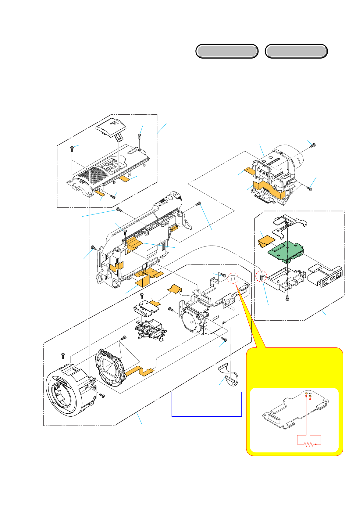
2-1-3. CABINET (L) BLOCK
EXPLODED VIEW
Follow the disassembly in the numerical order given.
1 VC-449 board (1-1 to 1-8)
2 Main flame block (2-1 to 2-7)
3 Switch block (3-1 to 3-2)
HARDWARE LIST
3Switch block control
3-1 (#5)
2-7 (#10)
3-2
1-1
1-2
1-3
2-3
2-4 (#5)
2-5 (#5)
2-2 (Claw)
2-6 (#14)
2-1 (#14)
1-8
(Claw)
1-6 (#3)
2 Main flame block
DCR-SR90E/SR100/SR100E_L2
1 VC-449 board
2-4
1-7 (#3)
1-4
1-5 (#3)
2-1-4. CABINET (R) BLOCK
EXPLODED VIEW
Follow the disassembly in the numerical order given.
1 CK-162 board (1-1 to 1-5)
2 R flame block (2-1 to 2-4)
3 LCD panel block (3-1 to 3-3)
1-4 (#3)
1-2
CK-162
1-3
1-5
2-2
(#12)
HARDWARE LIST
1 CK-162 board
3-3
1-1
2-1 (#5)
3-1 (#12)
2-4 (#10)
2-3 (#12)
2 R flame block
3-2
3 LCD panel block
DCR-SR90E/SR100/SR100E_L2
2-5
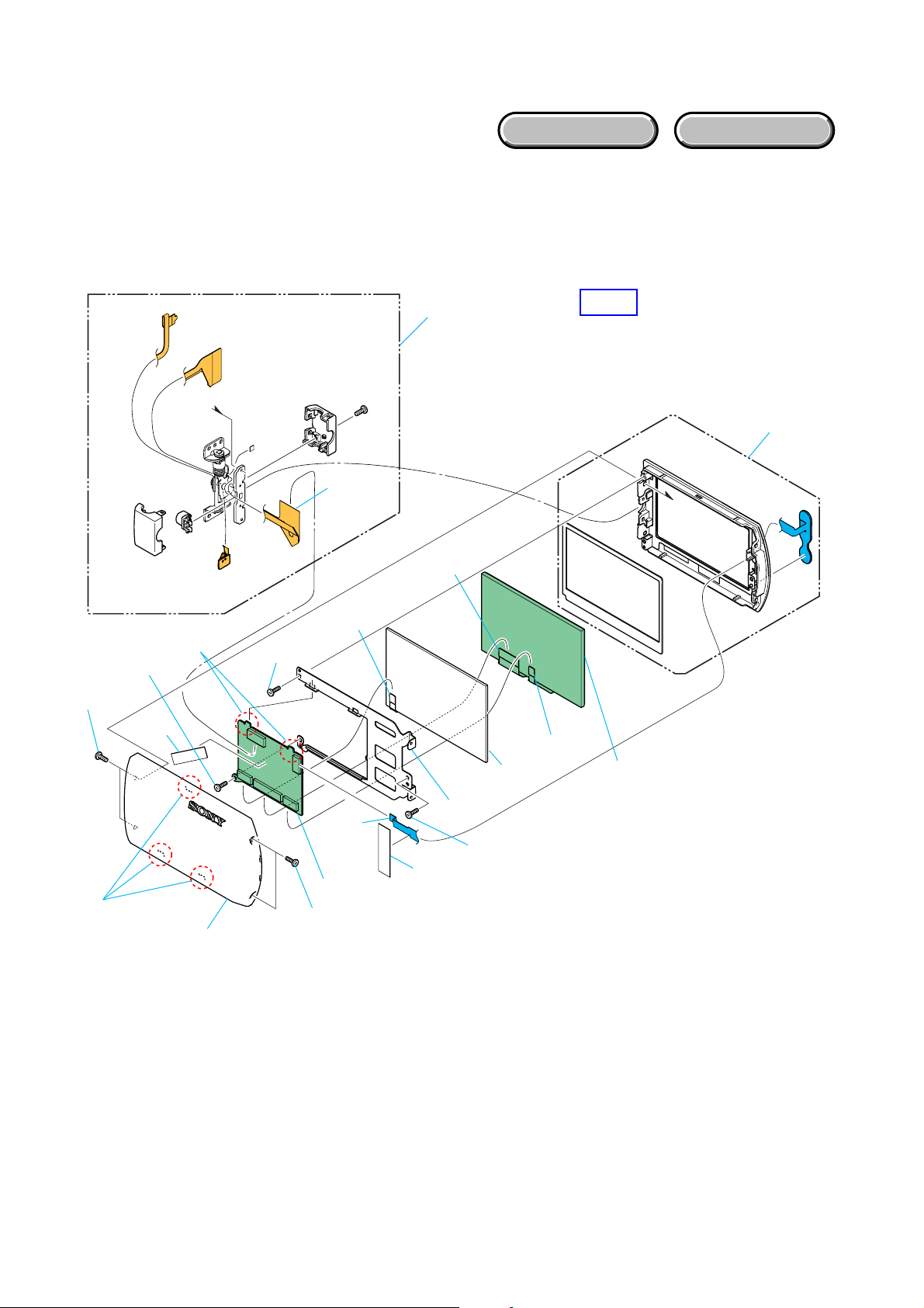
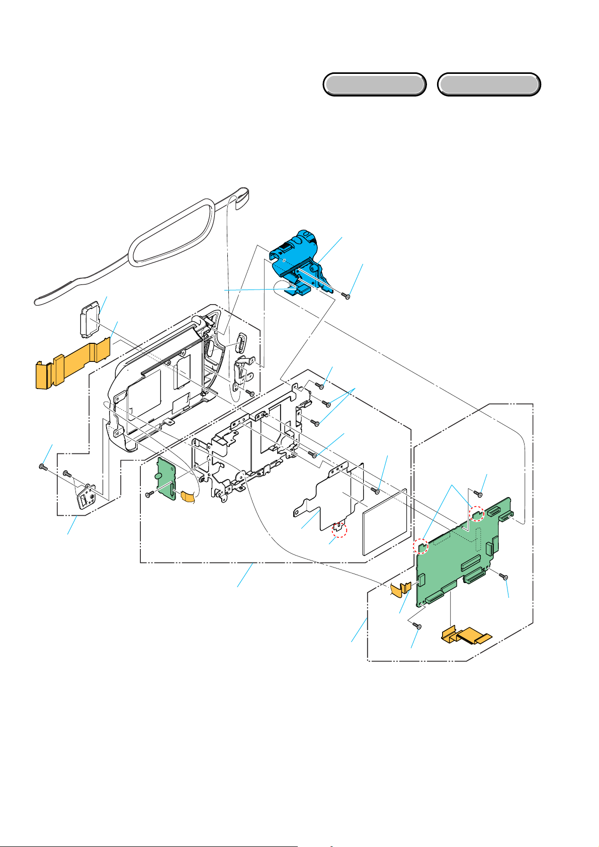
2-1-5. LCD BLOCK
EXPLODED VIEW
Follow the disassembly in the numerical order given.
1 Hinge block (1-1 to 1-6)
2 PD-250 board (2-1 to 2-7)
3 LCD (3-1 to 3-5)
HARDWARE LIST
2-6 (#5)
1-1 (#10)
2-7 (Claw)
1-5
3-1 (#5)
PD-250
1-6
2-3
1 Hinge block
2-4
3-4
HELP
3-5
2-5
3 LCD
1-3 (Claw)
1-4
DCR-SR90E/SR100/SR100E_L2
2-2
3-3
3-2 (#5)
2-1
2 PD-250 board
1-2 (#10)
2-6E
HELP
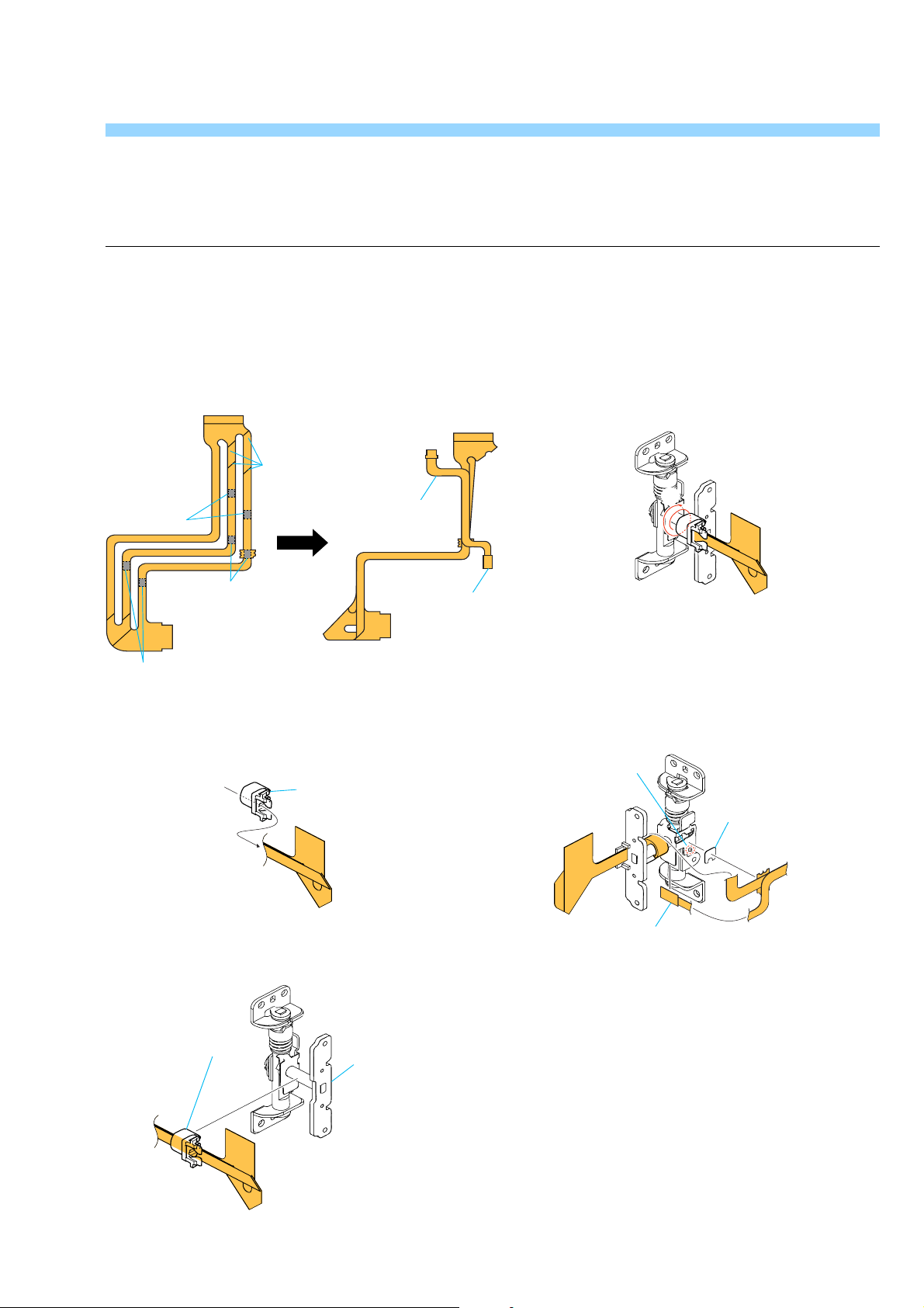
Sheet attachment positions and procedures of processing the flexible boards/harnesses are shown.
THE METHOD OF ATTACHMENT OF FP-439 FLEXIBLE BOARD
1 Fold dotted line parts of the FP-439 flexible board
as shown in figure.
2 Put the FP-432 flexible board on the FP-439
flexible board.
Fold
FP-432
Adhesive tape
Adhesive tape
Adhesive tape
3 Pass the FP-439 flexible board through
the FPC clamp(H).
FPC clamp(H)
Switch
5 Roll the the FP-439 flexible board 1.5 times,
in the direction of arrow
6 Put the adhesive sheet and FP-439 flexible
board on the hinge assy according to the
position of the boss and insert the switch of
the FP-432 flexible board as shown in figure.
Boss
A.
A
Adhesive tape
4 Install the FPC clamp(H) in the hinge assy.
FPC clamp(H)
DCR-SR90E/SR100/SR100E_L2
Switch
Hinge assy
HELP
Link
Link
3. BLOCK DIAGRAMS
OVERALL BLOCK DIAGRAM (1/5)
OVERALL BLOCK DIAGRAM (2/5)
OVERALL BLOCK DIAGRAM (3/5)
OVERALL BLOCK DIAGRAM (4/5)
OVERALL BLOCK DIAGRAM (5/5)
POWER BLOCK DIAGRAM (1/3)
POWER BLOCK DIAGRAM (2/3)
POWER BLOCK DIAGRAM (3/3)
DCR-SR90/SR100/SR100E_L2
3. BLOCK DIAGRAMS
3-1. O VERALL BLOCK DIAGRAM (1/5) ( ) : Number in parenthesis ( ) indicates the division number of schematic diagram where the component is located.
LENS BLOCK
IRIS
(SHUTTER)
IRIS
METER
M
H
ND FILTER
METER
M
H
FOCUS MOTOR
M
MR
ZOOM MOTOR
M
MR
NF MOTOR
M
LENS TEMP
SENSOR
CD-636 BOARD
Q5203
IC5202
CCD IMAGER
3 - 6, 16 - 19,
21 - 24
11
26
14
RG1, RG2,
LH11, LH12,
H1, H3, V1 - V4
67.5MHz: NTSC model
54MHz: PAL model
CLAMP
Q5204
CLAMP
X5201
Q5201
VOUT1
VOUT2
LT-041 BOARD FP-437 FLEXIBLE
CN8003
I_DRIVE+, -
7, 13. 514, 812, 1024 - 2718, 16 29, 2821, 1930 - 33
I_HALL+, -
ND_DRIVE+, -
ND_HALL+, -
FOCUS+, -
F_MR_A, B
ZOOM_A, B,
ZOOM_XA, XB
Z_MR_A, B
NF_DRIVE+, -
TEMP_OUT
23
23
BOARD
7, 13, 514, 812, 1024 - 2718, 16 29, 2821, 1930 - 33
13, 15
17, 25
31, 32
67, 69
71, 72
47
15
10
3, 22, 2, 23
33, 37, 38, 41
TIMING
GENERATOR
4
IC5205
S/H
IC5203
SHP1,2
SHD1, 2
VC-449 BOARD (1/5)
CN5201
18, 19
7, 6
9, 10, 12
53
66
57
2, 5, 1, 3
60
CN1701CN8002
I_DRIVE+, -
33, 3937, 35
I_HALL+, -
ND_DRIVE+, -
26, 3228, 30
ND_HALL+, -
FOCUS+, -
11, 1219, 21
F_MR_A, B
ZOOM_A, B,
ZOOM_XA, XB
16 - 1322, 24
Z_MR_A, B
NF_DRIVE+, -
10 - 76, 1
TEMP_OUT LENS_TEMP_AD
17
23
CCDout1P, 1N
28, 2925, 26
CCDout2P, 2N
TG_HD, VD, FLD
8 - 10
1
15
4, 5, 3, 6
CAM_DD_ON
CLPDM
CHCK
XSYS_RST
CSUB
H1, J1C5, B6
K2, L2
ND FILTER
C10, B11
F3, E3
B1, C4
K6, F1,
L4, G3
E12, E10
L6, L7
CN1501
8
2, 3
6, 5
23 - 21
30
16
CAM_SI, CAM_SO, CAM_SCK, CAM_CS
27, 26, 28, 25
1516
1813
IC1701
(2/15)
IRIS
DRIVE
K11, J11, H12, J12, L12
DRIVE
FOCUS
MOTOR
DRIVE
ZOOM
MOTOR
DRIVE
NF MOTOR
DRIVE
K12
K9, L9, M9, J9
H11
38, 4054, 52
IC1501
A/D
CONVERTER
(1/15)
8
CAM_SI, CAM_SO, CAM_SCK, CAM_CS, CAM_VD
SPCK
EN01,
DIR1A, DIR1B
XIC_1701_RST
17 - 30
1, 2, 61 - 72
14
CAM_SI, CAM_SO,
CAM_SCK, CAM_CS,
CAM_VD
AD1_0 - AD1_13
AD0_0 - AD0_13
AB11, Y11,
AB10, C22, A7
B14
R22
TG_FLD
D13
IC2601
(1/2)
CAMERA
CONTROL
(4/15)
TG_HD, TG_VD, TG_FLD
CAM_SI, CAM_SO,
CAM_SCK, CAM_CS,
CAM_VD
XSYS_RST
CAM_DD_ON
CLPDM
CLPOB
CHCK
CSUB
D14
B13
B8
F2
F4
M22
78
55 - 51,
49 - 45,
42 - 39
56 - 59,
62 - 71
77
92 - 90
137
99
23, 22, 20, 21, 25
SYS_V
IC_2803_CS
LINEOUT_V
XSYS_RST
ZOOM_VR_AD
IC1801
CAMERA SIGNAL
PROCESS
(3/15)
32, 108, 109
XSYS_RST
115
195 - 191,
188 - 185,
182 - 178,
175, 174
161 - 156,
153 - 148,
145, 144
167
101
102
122
24
SYS_V
IFI_Y0 - IFI_Y7
208 - 202, 199
IFI_C0 - IFI_C3
9 - 6
IFI_HD, IFI_VD, IF_OE
11 -13
VCK
MDQ0 - MDQ15
MA0 - MA11, BA0, BA1
MEMCK_OUT
STROBE_ON
EXT_STROBE_ON
CAM_SI, CAM_SO, CAM_SCK, CAM_VD
EN01, DIR1A, DIR1B
SPCK
SYS_V
IC_2803_CS
LINEOUT_V
LINEOUT_V
XSYS_RST
ZOOM_VR_AD
SYS_V
CAM_DD_ON
1
2
3
4
5
OVERALL (2/5)
(PAGE 3-2)
OVERALL (5/5)
(PAGE 3-5)
OVERALL (2/5)
(PAGE 3-2)
OVERALL (5/5)
(PAGE 3-5)
OVERALL (3/5)
(PAGE 3-3)
M9002
LENS COVER
MOTOR
IC001
LENS COVER
OPEN/CLOSE
SENSOR
M
3
2
MOTOR UNIT
(LENS BARRIER)
05
DCR-SR90E/SR100/SR100E_L2
CN8001
LENS_COVER_DRV+,
LENS_COVER_DRV-
8, 1
LENS_COVER_OPEN
4
LENS_COVER_CLOSE
3
A : VIDEO SIGNAL
A : AUDIO SIGNAL
36
37
34, 39
LENS_COVER_DRV+,
LENS_COVER_DRV-
LENS_COVER_OPEN
4
LENS_COVER_CLOSE
3
IC1702
LENS COVER
F3, F2
MOTOR DRIVE
(2/15)
LENS_COVER_DIR_PWM
C6
LENS_COVER_DRV_ON
B6
OVERALL (5/5)
(PAGE 3-5)
X2601
20MHz
EEP_SO
EEP_SI
EEP_SCK
XCS_EEP
XRST_VTR
5
2
32K EEPROM
6
1
IC2602
(4/15)
Y18
AB18
AC18
C1
B5
D5
PITCH_AD
7
YAW_AD
VST_C_RESET
P22
P23
T2
D1
AC14
AB14
AB13
F1
XRST_VTR
6
OVERALL (3/5)
(PAGE 3-3)
3-1
3-2. O VERALL BLOCK DIAGRAM (2/5) ( ) : Number in parenthesis ( ) indicates the division number of schematic diagram where the component is located.
VC-449 BOARD (2/5)
8
OVERALL (4/5)
(PAGE 3-4)
1
OVERALL (1/5)
(PAGE 3-1)
9
OVERALL (3/5)
(PAGE 3-3)
10
OVERALL (3/5)
(PAGE 3-3)
DCR-SR100/SR100E
AD4 - AD13
ADCK27
IFI_Y0 - IFI_Y7
IFI_C0 - IFI_C3
IFI_HD, IFI_VD, IF_OE
VCK
MDQ0 - MDQ15
MA0 - MA11, BA0, BA1
MEMCK_OUT
EVF_R
EVF_G
EVF_B
EVF_HD
EVF_VD
PANEL_R
PANEL_G
PANEL_B
PANEL_XHD
PANEL_XVD
DSCK_CNM
SPCK
Q2801
BUFFER
245
216 - 223224 - 227228 - 230
VIDEO/AUDIO DSP,
241
215 - 210,
208, 207,
205 - 198
185 - 176,
174, 173,
171, 170
196
47
46
52
95
96
40
39
45
92
93
IC2803
LENS CONTROL
(5/15)
264 - 267,
272, 273,
275, 276
301
298
284
304
62
33
66
64
53
60
89
82
83
85
87
91
3 - 10
279 - 282
268 - 270
2 4
DATA_FROM_SFD
IC2802
BUFFER
(5/15)
DATA_TO_SFD
CLPVO
VFE_C_OUT
ACC_CONT
AGC_CONT
IC_2803_Y_OUT
IC_2803_C_OUT
SFD_BCK
SFD_LRCK
SFD_FCK
KASYAON
ED0 - ED7
RCO0_EDHD, RCO1_EDVD,
RCO2_EDFLD, RCO3_FRMREF
RYI0_DE0 - RYI3_DE3, RCI0_DE4 - RCI3_DE7
RYO0_DEHD, RYO1_DEVD,
RYO2_DEFLD
ADATAIN0
ADATAOUT0
HYI_PLL27IN
MPLCK27
12
OVERALL (4/5)
(PAGE 3-4)
SFD_BCK
SFD_LRCK
SFD_FCK
13
OVERALL (4/5)
(PAGE 3-4)
AB15, AE17,
AA14, AB16,
AG17, AH19,
AA15, AG19
AD18,
AD17,
AB19,
AB18
AA18, AE20,
AD20, AG20,
AB17, AG21,
AD19, AE22
AH20,
AE18,
AE19
AA21
AB21
AH23
AB20
CODEC, USB I/F
AC5
AD22
AA20
Y22
IC2301
(1/2)
(6/15)
A13, A14,
B13 - B16,
D13 - D16,
E13 - E16,
G13, G14
D17,
B17,
E17
D18
D20
B28,
D25,
E25
B26
G18
E6
E7
B7
G5
D8
B8
J2
J1
GSENS_X,
GSENS_Y,
GSENS_Z
GSENS_TEMP
A23, A24
VBUS
SE981
3-AXIS
5 - 3
ACCELEROMETER
1
16
OVERALL (5/5)
(PAGE 3-5)
D2302
ATA_D0 - ATA_D15
ATA_A0 - ATA_A2
XATA_DMACK
XATA_RESET
HDD_ACCESS
USB_D+, USB_D-
USB_VBUS
MS_DIO
MS_SCLK
XMS_IN
MS_BS
MS_LED_ON
MS_VCC_ON
TXD4
RXD4
CN1107
CN1109
(1/3)
23
51
13
23
12
15
11
13
16
14
19
18
FP-431 FLEXIBLE
BOARD
DD0 - DD15
DA0 - DA2
17, 19, 16 34 - 49
DMCK-
-RESET
DASP-
FP-434
FLEXIBLE
BOARD (1/3)
18, 20
(FOR CHECK)
23
CN1105
CPC
HARD DISK
(30GB)
33, 31, 34 5 - 20
29
3
37
JK-310 BOARD
(1/3)
CN7201
(1/3)
D+, D-
28, 26
USB_VBUS
DRIVE
3, 2
1
CN7202
(USB)
EEP_TXD3
E11
EEP_RXD3
D10
EEP_SCK3
E10
XCS_EEP3
V2
SDDT0 - SDDT31
SDADR0 - SDADR11
BSDDT0 - BSDDT15
BSDADR0 - BSDADR12
E8
U2
MELODY_ENV
C1
14
15
CNMXCS_IC_2803
JAIRQ
DSCK_CNM
D0_CNM D15_CNM
XSYS_RST
D0_CNM - D15_CNM
A1_CNM - A23_CNM
IC2401
B5
64M FLASH
(7/15)
A1_CNM A23_CNM
B4
X2301
12MHz
SPCK
CAM_SI, CAM_SO,
CAM_SCK, CAM_VD
139
159, 158,
156, 236
3
OVERALL (1/5)
(PAGE 3-1)
11
OVERALL (4/5)
(PAGE 3-4)
05
EN01, DIR1A, DIR1B
SYS_V
IC_2803_CS
LINEOUT_V
MCXCS_IC_2803
BB_SI
BB_SO
XBB_SCK
248, 250, 251 252 - 261
157
154
164
149
152
151
150
144
147
D0_CNM - D15_CNM
137 - 124, 122, 121
A1_CNM - A19_CNM
116 - 98
119
141
XSYS_RST
D0_CNM - D15_CNM
A1_CNM - A20_CNM
OVERALL (5/5)
(PAGE 3-5)
OVERALL (4/5)
(PAGE 3-4)
AD16
P5
AB11 - AB13,
AD10 - AD13,
AE11 - AE13,
AG11 - AG13,
AH11 - AH13
AB9,
AD6 - AD9,
AE5 - AE9,
AG4 - AG10,
AH4 - AH9,
AA22
A21
A22
3
6
64K EEPROM
2
7
Q2301, 2302
MODULATOR
IC2303
(6/15)
IC2403
128M SDRAM
(7/15)
IC2402
256M SDRAM
(7/15)
SHOE_CONT
BEEPMELODY
17
18
OVERALL (5/5)
(PAGE 3-5)
OVERALL (4/5)
(PAGE 3-4)
A : VIDEO SIGNAL
A : AUDIO SIGNAL
A : VIDEO/AUDIO SIGNAL
DCR-SR90E/SR100/SR100E_L2
3-2
3-3. O VERALL BLOCK DIAGRAM (3/5) ( ) : Number in parenthesis ( ) indicates the division number of schematic diagram where the component is located.
VC-449 BOARD (3/5)
OVERALL (1/5)
(PAGE 3-1)
OVERALL (4/5)
(PAGE 3-4)
OVERALL (2/5)
(PAGE 3-2)
OVERALL (4/5)
(PAGE 3-4)
05
19
10
20
FP-441 FLEXIBLE
CN1103
PANEL_R
PANEL_G
PANEL_B
PANEL_HD
PANEL_VD
BB_SI
BB_SO
XBB_SCK
XCS_LCD
TP_X
TP_Y
TP_SEL1
BOARD
6
7
8
4
5, 9 - 18
1
CN7301
FP-439
FLEXIBLE
BOARD
1
2
3
19
17
7 7 3
EVF_R
EVF_G
9
OVERALL (2/5)
(PAGE 3-2)
6
XRST_VTR
BB_SI
BB_SO
XBB_SCK
XCS_EVF
XCS_LCD
EVF_BL_ON
XCS_IC_3401
PANEL_R
PANEL_G
PANEL_B
PANEL_XHD
PANEL_XVD
DSCK_CNM
SPCK
IC_2201_Y_OUT_M
IC_2201_C_OUT_M
13
11
10
12
40
38
36
3
4
7
19
42
44
IC3401
ASPECT RATIO
CONVERTER
(8/15)
OVERALL (4/5)
(PAGE 3-4)
OVERALL (4/5)
(PAGE 3-4)
OVERALL (5/5)
(PAGE 3-5)
OVERALL (5/5)
(PAGE 3-5)
OVERALL (5/5)
(PAGE 3-5)
OVERALL (1/5)
(PAGE 3-1)
OVERALL (5/5)
(PAGE 3-5)
5
Q3401
30
28
26
22
23
32
34
BUFFER
IC_3401_Y
IC_3401_C
22
23
25
26
29
5
27
EVF_B
EVF_HD
EVF_VD
BB_SI
BB_SO
HI_SO
HI_SI
XHI_SCK
XCS_IC_2601
ADDO
ADDE
A5.1_SYNC
XCS_A5.1
A5.1_CTRL
A5.1_RESET
XDSP_NMI
HI_TXD0
HI_RXD0
HI_SCK0
HI_CS
OSD_V
XHIDSCON_MAD
XFUPSTAT
XCNM_RESET
IR_ON
SCHARGE_ON
XSCHARGE_FULL
ADAPTER_DETECT
SYS_V
CAM_DD_ON
CAM_DD_ON
XBATT_VIEW
HI_XRESET
PANEL_REVERSE
NIGHTSHOT_SW
XCS_LCD
XBB_SCK
OVERALL (4/5)
XBB_SCK
XCS_EVF
XRST_VTR
EVF_BL_ON
PANEL_R_M
PANEL_G_M
PANEL_B_M
PANEL_XHD_M
PANEL_XVD_M
21
(PAGE 3-4)
G9
H8
H7
V4
AF2
AC4
AD4
AB7
G4
F1
D12
G11
H10
H11
H9
N4
D1
A12
AC2
E4
F4
C2
B2
P4
G7
34
33
32
48
BB_SI
42
BB_SO
45
44
43
IC2301
(2/2)
DS/HI CONTROL
(6/15)
IC5102
EVF DRIVE
(11/15)
1
3
B24
D24
D5
D6
A27
B27
TP_X
TP_Y
TP_SEL_2
TP_SEL_1
20
21
22
26
16, 17, 24, 30
6 - 10, 12, 14,
EXTDA
31
SWITCHING
Q1102
EVF_HCK1, EVF_HCK2,
EVF_PSIG, EVF_REF, EVF_STB
IC5101
EVF BACKLIGHT
1 4
CONTROL
(11/15)
CN1104
(1/2)
PANEL_R
PANEL_G
PANEL_B
PANEL_HD
PANEL_VD
BB_SI
BB_SO
XBB_SCK
XCS_LCD
KEY_AD1 KEY_AD1
KEY_AD3
XBATT_VIEW
HI_XRESET
KEY_AD2
PANEL_REV
30
28
26
18 22 13 13
17 23 14 14
9 31 20 20
6 34 23 23
7 33 22 22
8 32 21 21
TP_X
10
TP_Y
12
TP_SEL1
11
24
33
37
38
1 39
2 38
Q5102
EVF BACKLIGHT
DRIVE
FP-440
FLEXIBLE
BOARD (1/2)
EVF_VR
EVF_VG
EVF_VB
EVF_COM_CS
EVF_HST, EVF_PCG,
EVF_EN, EVF_VCK,
EVF_VST, EVF_BLK,
LED_K
CK-162 BOARD (1/2)
CN7305
(1/2)
10
12
14
30
28
29 18 18
16
7
S7302
DISP/
BATT INFO
3
2
S7301
RESET
6
7
8
4
1
S7306
DVD BURN
S7303
EASY
S7305
WIDE
SELECT
S7304
PANEL
OPEN/CLOSE
VF-176 BOARD
CN5801
HCK1, HCK2,
HST, PCG, EN,
VCK, VST, BLK,
PSIG, REF, STB
5, 9 - 18
D5802
(EVF BACKLIGHT)
PD-250 BOARD
CN7501
PANEL_R
1
PANEL_G
2
PANEL_B
3
PANEL_HD
PANEL_VD
VD_SI
VD_SO
VD_SCK
XCS_LCD
19
17
CN7303
KEY_AD3
KEY_AD4
6
1
CN7302
CN5802
VR
17
VG
18
VB
16
COM
21
CS
19
5 - 7, 9 - 16, 20
37
36
35
IC7501
LCD DRIVE
52
2
6 - 13,
16, 18,
26, 31
20 34
EXTDA
BL_ON
BACKLIGHT
DRIVE
NS-021 BOARD
CN8601
1
6
D_2.8V
FP-442
FLEXIBLE
BOARD
BACK_LIGHT
NIGHT_SHOT
46
49
48
47
Q7513 - 7516
FP-432 FLEXIBLE BOARD
S001
5, 6
PANEL REVERSE
DETECT
LCD9002
COLOR
EVF UNIT
22
23
24
29
ON
OFF
Q7501, 7502
S8601
BACK LIGHT
S8602
NIGHTSHOT
HCK1, HCK2, HST,
PCG, EN, VCK,
VST, PSIG, REF,
XSTBY, DWN, RGT
TP_TOP
TP_BOT
SWITCHING
KEY_AD1
KEY_AD1_2
KEY_AD1_1
A : VIDEO SIGNAL
CN7505
R
4
G
5
B
3
2, 6 - 8, 11 - 14, 19 - 22
COM
24
CS
23
COM
1
CN7503
5
TP_L
2
TP_R
1
4
CN7506
BL_H
5, 6
CONTROL KEY BLOCK
(SB9000)
CN7502
4
5
LCD9001
2.7INCH
WIDE COLOR
LCD UNIT
TOUCH PANEL
D9001
(BACKLIGHT)
S003
START/STOP
S002
T
S001
W
DCR-SR90E/SR100/SR100E_L2
3-3
3-4. O VERALL BLOCK DIAGRAM (4/5) ( ) : Number in parenthesis ( ) indicates the division number of schematic diagram where the component is located.
VC-449 BOARD (4/5)
8
OVERALL (2/5)
(PAGE 3-2)
DCR-SR100/SR100E
AD4 - AD13
ADCK27
13
OVERALL (2/5)
(PAGE 3-2)
18
OVERALL (2/5)
(PAGE 3-2)
IC3801
VIDEO A/D
24 - 15
CONVERTER
14
(9/15)
DATA_FROM_SFD
SFD_BCK
SFD_LRCK
SFD_FCK
KASYAON
BEEP
5
1
LINE_Y_ON
DATA_TO_SFD
20
OVERALL (3/5)
(PAGE 3-3)
AIN
12
OVERALL (2/5)
(PAGE 3-2)
21
OVERALL (3/5)
(PAGE 3-3)
DATA_TO_SFD
DATA_FROM_DSP
IC_2201_ C_OUT_M
IC_2201_ Y_OUT_M
CLPVO
VFE_C_OUT
ACC_CONT
AGC_CONT
IC_2803_Y_OUT
IC_2803_C_OUT
IC_3401_Y
IC_3401_C
IC2203
7
AUDIO
SELECTOR
6
(9/15)
5
DSP_SEL
91
12
10
11
8
Q2202
BUFFER
Q2203
BUFFER
Q3801
BUFFER/
CLAMP
IC2202
AUDIO
A/D, D/A
CONVERTER
(9/15)
14 13 6 7
XPWDA
XPWAD1
DEM0
DEM1
A : VIDEO SIGNAL
A : AUDIO SIGNAL
DCR-SR100/SR100E
IC2201
I/O
(9/15)
12
17
14
88
3
90
57
61
PMUTE_L
58
PMUTE_R
60
55
56
70
74
23
24
XCS_IC_2201_1
25
27
BB_SO
XBB_SCK
SDC_IN
28
OVERALL (5/5)
(PAGE 3-5)
CN1109
S_Y_I/O
S_C_I/O
VIDEO_I/O
AUDIO_L_I/O
AUDIO_R_I/O
LANC_SIG
MULTI_JACK_IN
CN1104
SP+
SP-
(2/3)
(2/2)
FP-434
FLEXIBLE
BOARD (2/3)
14
12
10
2
4
6
7
34
35
FP-440
FLEXIBLE
BOARD (2/2)
JK-310 BOARD (2/3)
CN7201
(2/3)
32
34
36
44
42
40
39
CN7305
(2/2)
6
5
CK-162 BOARD
(2/2)
S_Y
S_C
VIDEO_IN/OUT
AUDIO_L
AUDIO_R
LANC_SIG
JACK_AD
CN7304
SP+
SP-
10
5
9
CN7203
A/V
1
6
2
7
1
2
SP9001
SPEAKER
19
21
20
18
10
7
9
6
VIDEO, AUDIO
PBIN_L
15
PBIN_R
16
3
2
MIC_L
MIC_R
RECOUT_L
RECOUT_R
BEEP
31
30
35
34
65
51
52
MICROPHONE
CN9001
(1/2)
HOT SHOE
UNIT
(L)
FRONT
(R)
(L)
REAR
(R)
FP-436
FLEXIBLE
BOARD
(1/2)
MIC_FL
MIC_FR
MIC_RL
MIC_RR
MA-444 BOARD (1/2)
CN5002
7
3
1
5
CN5003
3
2
6
5
(1/2)
INIT_
MIC_F
INIT_
MIC_B
SHOE_MIC_RL
SHOE_MIC_RR
B8
A1
B7
B2
B8
A1
B7
B2
IC3301
MIC AMP
(1/3)
H3H3G5
IC3351
SUB MIC
AMP
(2/3)
G6
H2
ZOOM_MIC_CONT
SHOE_STEREO
SUB_RECOUT_L
G6
SUB_RECOUT_R
H2
CN5004
MIC_L
MIC_R
(1/2)
FP-435
FLEXIBLE
BOARD
(1/2)
39
37
32 14
33 13
43
41
31 15
CN1102
(1/2)
MIC_L
7
MIC_R
9
ZOOM_MIC
_CONT
SHOE_STEREO
SUB_RECOUT_L
3
SUB_RECOUT_R
5
SHOE_MIC_FLSHOE_MIC_FL
LINE_Y_ON
SFD_FCK
SFD_LRCK
SFD_BCK
3
2
MIC (REAR)
12
CONVERTER
10
11
3
2
WIRELESS
12
CONVERTER
10
11
OVERALL (2/5)
(PAGE 3-2)
IC2903
A/D
(10/15)
IC3551
MIC A/D
(10/15)
15
DATA_TO_SFD
SFD_BCK
SFD_LRCK
SFD_FCK
8 R4
13
8 R9
13
DATA_TO_DSP
XPWAD2
WMIC_DATA
XPWAD3
D0_CNM - D15_CNM
A1_CNM - A20_CNM
U6
R7, U2, U3,
U7, U8, V17
R3, R8, T5,
T9, U15, V9
G17
IC2901
5.1CH AUDIO
DSP
(10/15)
A10, A16, A17,
B11, B13 - B16
C11 - C15, C17,
D11, D13
E16 - E18, F15, F17,
G15, G16, G18, H16, H18,
J17, J18, K16 - K18,
L17, L18, N16, P17, P18
U10
R13
U16
M4
D17
P16
H17
U12
DATA_FROM_DSP
ADDO
ADDE
A5.1_SYNC
XCS_A5.1
A5.1_CTRL
A5.1_RESET
XDSP_NMI
XCS_IC_2201_1
SDC_IN
DSP_SEL
XPWDA
XPWAD1
DEM0
DEM1
ZOOM_MIC_CONT
SHOE_STEREO
LINE_Y_ON
XPWAD2
XPWAD3
23
OVERALL (3/5)
(PAGE 3-3)
U2
U23
B4
L20
Y17
AC10
L23
AB17
W22
W20
B3
A4
IC2601
(2/2)
CAMERA
CONTROL
(4/15)
E23
AC8
AB8
AC7
U1
R4
B20
F20
AB7
Y7
AB6
AC6
BB_SO
XBB_SCK
MCXCS_IC_2803
BB_SI
BB_SO
XBB_SCK
BB_SI
BB_SO
XBB_SCK
XCS_EVF
XCS_LCD
EVF_BL_ON
XCS_IC_3401
HI_SO
HI_SI
XHI_SCK
XCS_IC_2601
11
OVERALL (2/5)
(PAGE 3-2)
19
OVERALL (3/5)
(PAGE 3-3)
22
OVERALL (3/5)
(PAGE 3-3)
DCR-SR90E/SR100/SR100E_L2
05
3-4
 Loading...