

Sony CXP875P40 Datasheet

CMOS 8-bit Single Chip Microcomputer
Description
The CXP875P40 is a CMOS 8-bit micro-computer
which consists of arithmetic coprocessor, A/D
converter, serial interface, timer/counter, time base
timer, vector interruption, high precision timing
pattern generation circuit, PWM generator and the
measuring circuit which measure signals of capstan
FG, drum FG/PG, reel FG and other servo systems,
as well as basic configurations like 8-bit CPU,
PROM, RAM and I/O port. They are integrated into a
single chip.
Also this IC provides power on reset function,
sleep/stop function which enables to lower power
consumption.
The CXP875P40 is the one-chip PROM version of
the CXP87532/87540 with mask ROM, providing the
function of being able to write directly into the
program. It is suitable for evaluation use during
system development and for small quantity
production.
100 pin QFP (Plastic)
Structure
Silicon gate CMOS IC
CXP875P40
100 pin LQFP (Plastic)
Features
• A wide instruction set (213 instructions) which cover various types of data
— 16-bit operation code/multiplying instruction/boolean bit operation instruction
• Minimum instruction cycle During operation 326ns/12.288MHz
• Incorporated PROM capacity 40K bytes
• Incorporated RAM capacity 1344 bytes
• Peripheral functions
— Arithmetic coprocessor Multiplying with code, sum of products with code, high speed
execution of many bits shift rotation operation
— A/D converter 8-bit, 8-channel, successive approximation system
(Conversion time 13µs/12.288MHz)
Incorporated 3-stage FIFO for A/D conversion data
— Serial interface Incorporated buffer RAM for data
(1 to 128 bytes auto transfer) 2-channel
— Timer 8-bit timer, 8-bit timer/counter, 19-bit time base timer
— High precision timing pattern generator PPG (11 pins) 32-stage programmable
— PWM output 12-bit, 2-channel (Repeated frequency 48kHz)
8-bit, 3-channel (Repeated frequency 48kHz)
— Servo input control Capstan FG, Drum FG/PG, Reel FG input
— FRC capture unit Incorporated 28-bit and 8-stage FIFO
• Interruption 12 factors, 12 vectors, multi-interruption possible
• Standby mode SLEEP/STOP
• Package 100-pin plastic QFP/LQFP
Sony reserves the right to change products and specifications without prior notice. This information does not convey any license by
any implication or otherwise under any patents or other right. Application circuits shown, if any, are typical examples illustrating the
operation of the devices. Sony cannot assume responsibility for any problems arising out of the use of these circuits.
– 1 –
E94317-PS

CXP875P40
V
PP
V
SS
V
DD
MP
RST
XTAL
EXTAL
NM1
PE1/INT2
PE3/INT1
PE0/INT0
PA0 to PA7
CLOCK GENERATOR/
PB0 to PB7
PORT A
SYSTEM CONTROL
SPC700
PORT B
CPU CORE
CO-PROCESSOR
PC0 to PC7
PORT C
RAM
1120 BYTES
PROM
40K BYTES
PD0 to PD7
PE0 to PE1
PORT D
PF0 to PF7
PE2 to PE7
PORT E
PORT F
PRESCALER/
TIME BASE TIMER
FRC
INTERRUPT CONTROLLER
PG0 to PG7
PORT G
FIFO
UNIT
CAPTURE
PH0 to PH3
PH4 to PH7
PORT H
PORT I
PJ0 to PJ7
PORT J
PI0 to PI7
RAM
PATTERN
GENERATOR
PROGRAMMABLE
PK0 to PK3
PORT K
PA2/PPO10
to
PB0/PPO0
8BIT PWM GENERATOR 3CH
PE2/PWM0
PE3/PWM1
Block Diagram
FIFO
A/D CONVERTER
12BIT PWM GENERATOR 2CH
8
DD
AV
AVSS
AVREF
PF0/AN0
PE5/PWM3
PE6/PWM4
to PF7/AN7
PA4/ATFS1
PA5/ATFS3
PE4/PWM2
ATF SYNC UNIT
PK0/RFDT
PK1/MCLK
PA7/ATFS2
6
SERVO
GENRATOR
SWITCHING PULSE
PE7/SWP
PA6/AREA
DRUM
PG3/DPG
PG4/DFG
PG2/DREF
– 2 –
INPUT
CONTROL
REEL
CAPSTAN
PG5/CFG
PG6/RFG0
PG7/RFG1
PA3/PROUT
SI0
CS0
PG0/EXI0
PG1/EXI1
RAM
UNIT
SERIAL
INTERFACE
SO0
SCK0
PH2/SI1
PH3/CS1
8BIT TIMER 1
8BIT TIMER/COUNTER 0
PE1/EC
PH1/SO1
PH0/SCK1
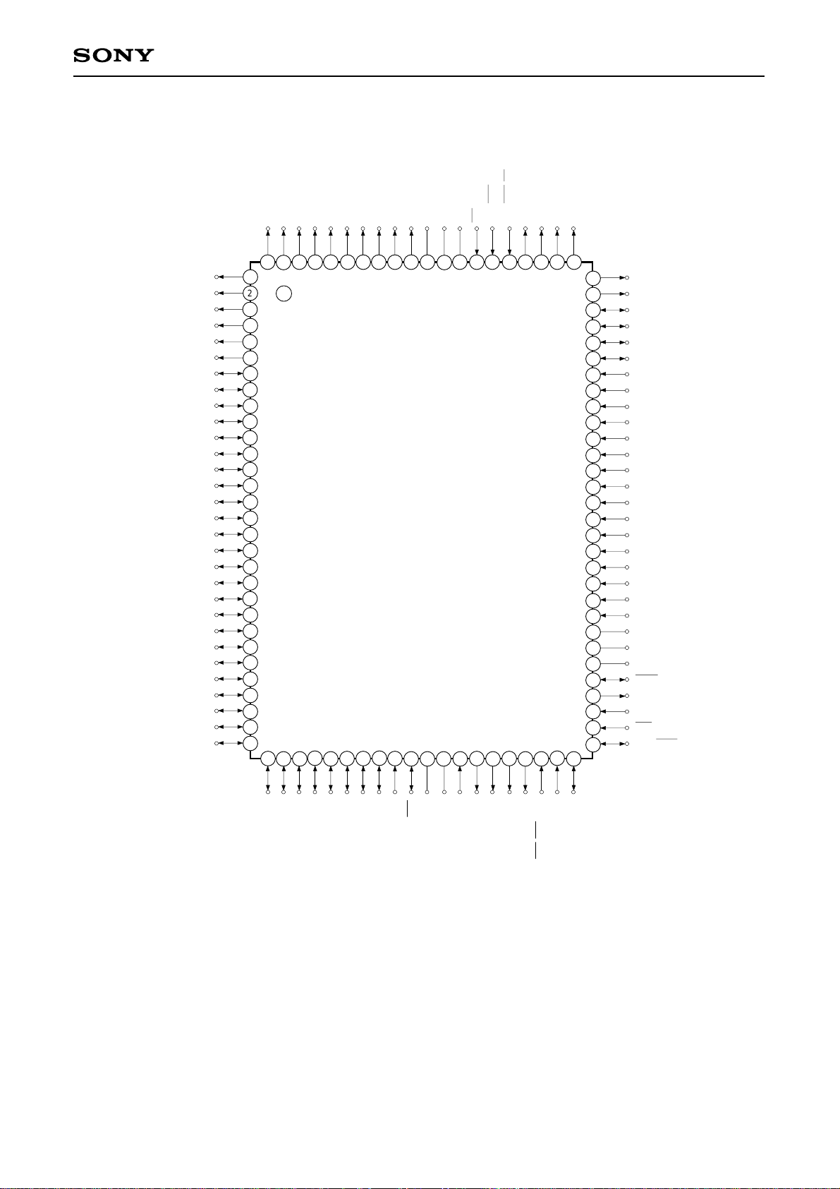
Pin Configuration 1 (Top View) 100pin QFP
PA0/PPO8
PA1/PPO9
PB7/PPO7
PB6/PPO6
PA2/PPO10
PA4/ATFS1
PA5/ATFS3
PA3/PROUT
PP
PA6/AREA
PA7/ATFS2
V
CXP875P40
DD
SS
V
V
PE0/INT0
NMI
PE3/PWM1
PE1/INT2/EC
PE2/PWM0
PE4/PWM2
PE5/PWM3
PPO5/PB5
PPO4/PB4
PPO3/PB3
PPO2/PB2
PPO1/PB1
PPO0/PB0
PC7
PC6
PC5
PC4
PC3
PC2
PC1
PC0
PD7
PD6
PD5
PD4
PD3
PD2
PD1
PD0
PI7
PI6
PI5
PI4
PI3
PI2
PI1
PI0
95
93
94
92
97
96
98
100
99
1
2
3
4
5
6
7
8
9
10
11
12
13
14
15
16
17
18
19
20
21
22
23
24
25
26
27
28
29
30
34
31
32
35
33
38
36
37
90
91
41
40
39
87
86
88
89
44
43
42
45
83
84
85
46
82
81
80
79
78
77
76
75
74
73
72
71
70
69
68
67
66
65
64
63
62
61
60
59
58
57
56
55
54
53
52
51
49
48
47
50
PE6/PWM4
PE7/SWP
PK0/RFDT
PK1/MCLK
PK2
PK3
PG0/EXI0
PG1/EXI1
PG2/DREF
PG3/DPG
PG4/DFG
PG5/CFG
PG6/RFG0
PG7/RFG1
PF0/AN0
PF1/AN1
PF2/AN2
PF3/AN3
PF4/AN4
PF5/AN5
PF6/AN6
PF7/AN7
AV
DD
AVREF
AVSS
SCK0
SO0
SI0
CS0
PH0/SCK1
SS
MP
PJ7
PJ6
PJ5
PJ4
PJ3
PJ2
PJ1
PJ0
RST
V
XTAL
PH7
EXTAL
PH6
PH5
PH4
Note) 1. VPP (Pin 90) is always connected to VDD.
2. VSS (Pins 41 and 88) are both connected to GND.
3. MP (Pin 39) is always connected to VSS.
– 3 –
SI1/PH2
SO1/PH1
CS1/INT1/PH3
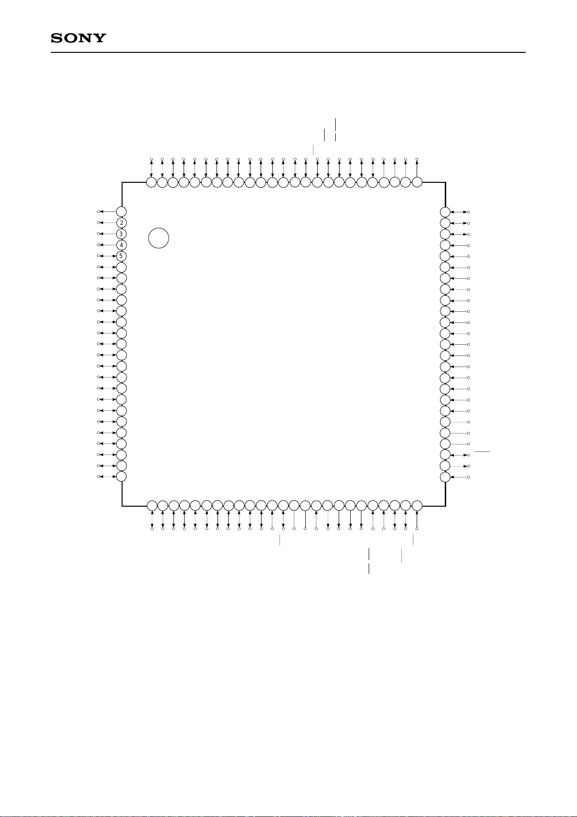
Pin Configuration 2 (Top View) 100pin LQFP
PA0/PPO8
PA2/PPO10
PA3/PROUT
PB5/PPO5
PB4/PPO4
PB6/PPO6
PA1/PPO9
PB7/PPO7
PA4/ATFS1
PA5/ATFS3
PA6/AREA
PA7/ATFS2
CXP875P40
PP
DD
SS
PE0/INT0
V
NMI
PE1/EC/INT2
V
V
PE2/PWM0
PE3/PWM1
PE6/PWM4
PE5/PWM3
PE4/PWM2
PE7/SWP
PK0/RFDT
PBO3/PB3
PPO2/PB2
PPO1/PB1
PPO0/PB0
PC7
PC6
PC5
PC4
PC3
PC2
PC1
PC0
PD7
PD6
PD5
PD4
PD3
PD2
PD1
PD0
PI7
PI6
PI5
PI4
PI3
95
93
94
92
97
96
98
100
99
1
2
3
4
5
6
7
8
9
10
11
12
13
14
15
16
17
18
19
20
21
22
23
24
25
90
91
87
86
84
88
89
85
81
83
82
78
76
80
77
79
75
74
73
72
71
70
69
68
67
66
65
64
63
62
61
60
59
58
57
56
55
54
53
52
51
PK1/MCLK
PK2
PK3
PG0/EXI0
PG1/EXI1
PG2/DREF
PG3/DPG
PG4/DFG
PG5/CFG
PG6/RFG0
PG7/RFG1
PF0/AN0
PF1/AN1
PF2/AN2
PF3/AN3
PF4/AN4
PF5/AN5
PF6/AN6
PF7/AN7
AV
DD
AVREF
AVSS
SCK0
SO0
SI0
PJ5
34
PJ4
35
33
PJ2
PJ3
32
29
31
30
28
27
26
PI2
PI1
PI0
PJ6
PJ7
PJ1
38
PJ0
39
37
MP
RST
41
40
SS
V
XTAL
36
42
PH7
EXTAL
44
43
PH6
PH5
Note) 1. VPP (Pin 88) is always connected to VDD.
2. VSS (Pins 39 and 86) are both connected to GND.
3. MP (Pin 37) is always connected to VSS.
– 4 –
46
45
PH4
49
48
47
SI1/PH2
SO1/PH1
SCK1/PH0
CS1/INT1/PH3
50
CS0
Pin Description
Symbol I/O Description
CXP875P40
PA0/PPO8
PA1/PPO9
PA2/PPO10
PA3/PROUT
PA4/ATFS1
PA5/ATFS3
PA6/AREA
PA7/ATFS2
PB0/PPO0
to
PB7/PPO7
PC0 to PC7
PD0 to PD7
PE0/INT0
Output/
Real time output
Output/
Monitor output
Output/
Real time output
I/O
I/O
Input/Input
(Port A)
8-bit output port.
Data is gated with PPO
Programmable pattern generator (PPG)
Output (3 pins) and capstan servo control
signal (1 pin).
(3 pins), monitor signal
(4 pins) in relation to ATF,
control signal (1 pin) for
capstan servo by OR-gate
Monitor output in relation to ATF.
(4 pins)
and they are output. (8 pins)
(Port B)
8-bit output port. Data is gated
with PPO by OR-gate and
Programmable pattern generator (PPG)
output. (8 pins)
they are output. (8 pins)
(Port C)
8-bit input/output port, enables to specify input/output by 4-bit unit.
(8 pins)
(Port D)
8-bit input/output port. Lower 4 bits can be specified as input/output by
bit unit and upper 4 bits can be specified as input/output by 4-bit unit.
(8 pins)
Input pin to request external interruption.
Active when falling edge.
PE1/EC/INT2
PE2/PWM0
to
PE6/PWM4
PE7/SWP
PF0/AN0
to
PF7/AN7
PG0/EXI0
PG1/EXI1
PG2/DREF
PG3/DPG
PG4/DFG
PG5/CFG
PG6/RFG0
PG7/RFG1
Input/Input/
Input
Output/Output
Output/Output
Input/Input
Input/Input
Input/Input
Input/Input
Input/Input
Input/Input
Input/Input
Input/Input
Input/Input
(Port E)
8-bit port. Lower 2 bits
are input pins and upper
6 bits are output pins.
(8 pins)
(Port F)
8-bit input port. (8 pins)
Upper 4 bits serve as
standby release input pin.
(Port G)
8-bit input port.
(8 pins)
External event
input pin for
timer/counter.
Input pin to request external
interruption. Active when
falling edge.
PWM output pins (5 pins)
SWP output pin.
Analog input pins to A/D converter.
(8 pins)
External input pin 0.
External input pin 1.
Drum reference signal input pin.
Drum PG input pin.
Drum FG input pin.
Capstan FG input pin.
Reel FG input pin.
– 5 –

Symbol I/O Description
CXP875P40
PH0/SCK1
PH1/SO1
PH2/SI1
PH3/INT1/
CS1
PH7 to PH4
PI0 to PI7
PJ0 to PJ7
PK0/RFDT
PK1/MCLK
PK2 to PK3
SCK0
SO0
SI0
CS0
NMI
EXTAL
XTAL
Input/I/O
Input/Output
Input/Input
Input/Input/Input
Output
I/O
I/O
I/O/Input
I/O/Input
I/O
I/O
Output
Input
Input
Input
Input
Output
(Port H)
4-bit input port.
(4 pins)
Serial clock input/output pin.
Serial data output pin.
Serial data input pin.
Input pin to request
external interruption.
Chip select input pin to serial interface.
Active when falling edge.
(Port H)
4-bit output port. N-ch open drain output of middle tension proof (12V)
and high current (12mA). (4 pins)
(Port I)
8-bit input/output port, enables to specify input/output by 4-bit unit.
(8 pins)
(Port J)
8-bit input/output port, enables to specify input/output by 4-bit unit.
(8 pins)
(Port K)
4-bit input/output port,
enables to specify input/
Playback data input pin.
Channel clock input pin.
output by bit unit. (4 pins)
Serial clock input/output pin.
Serial data output pin.
Serial data input pin.
Chip select input pin to serial interface.
Non-maskable interrupt request pin. Active during falling edge.
Connecting pin of crystal oscillator for system clock. When supplying
the external clock, input the external clock to EXTAL pin and set XTAL
pin to open.
RST
MP
AVDD
AVREF
AVSS
VDD
VPP
VSS
I/O
Input
Input
System reset pin of active “L” level. RST pin is input/output pin, which
output “L” level by incorporated power on reset function when power
ON. (Mask option)
Test mode pin. This pin is always connected to GND.
Positive power supply pin of A/D converter.
Set the same voltage as VDD.
Reference voltage input pin of A/D converter.
GND pin of A/D converter.
Positive power supply pin.
Positive power supply pin for incorporated PROM writing.
In normal operation, connect to VDD.
GND pin. Connect both VSS pins to GND.
– 6 –
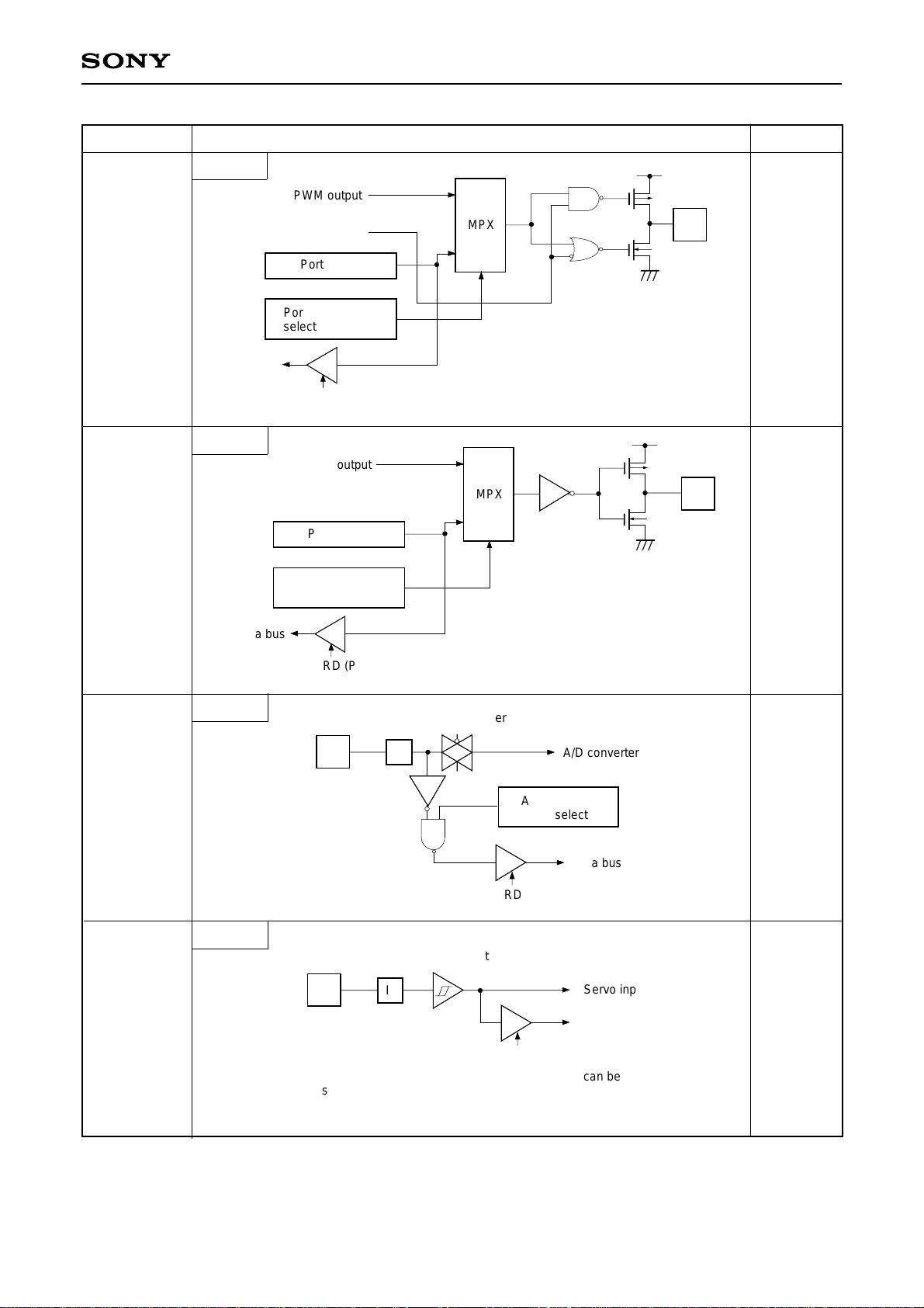
I/O Circuit Formats for Pins
Pin Circuit format When reset
CXP875P40
PA0/PPO8
to
PA2/PPO10
PA3/PROUT
PA4/ATFS1
PA5/ATFS3
PA6/AREA
PA7/ATFS2
PB0/PPO0
to
PB7/PPO7
16 pins
PC0
to
PC7
8 pins
Port A
Port B
Port C
Data bus
PPO, PROUT,
ATFS1 to ATFS3,
AREA, data
Port A or Port B
Data bus
Port C data
Port C direction
RD (Port C)
RD
Output becomes active from high impedance
by data writing to port register.
Input protection
IP
(Every 4 bits)
Buffer
circuit
Hi-Z
Hi-Z
PD0
to
PD7
8 pins
PE0/INT0
PE1/EC/
INT2
Port D
Data bus
Port E
Port D data
Port D direction
RD (Port D)
Schmitt input
IP
Lower 4 bits are by bit unit
and upper 4 bits are by 4bit unit
Data bus
RD (Port E)
Large current
12mA
IP
Hi-Z
Hi-Z
2 pins
– 7 –
A
A
A
A
Pin Circuit format When reset
Port E
PWM output
MPX
A
A
PE2/PWM0
PE3/PWM1
PE4/PWM2
PE5/PWM3
Hi-Z control
Port E data
Port/PWM output
select
Data bus
CXP875P40
Hi-Z
4 pins
PE6/PWM4
PE7/SWP
2 pins
PF0/AN0
to
PF7/AN7
Port E
Data bus
Port F
RD (Port E)
PWM, SWP output
Port E data
Port/PWM, SWP
output select
RD (Port E)
Input multiplexer
IP
A
MPX
A
A/D converter
Analog/Digial
tinput select
H level
Hi-Z
8 pins
PG0/EXI0
PG1/EXI1
PG2/DREF
PG3/DPG
PG4/DFG
PG5/CFG
PG6/RFG0
PG7/RFG1
8 pins
Port G
Data bus
RD (Port F)
Schmitt input
IP
RD (Port G)
For PG0/EXI0 to PG7/RFG1, TTL schmitt input can be
selected with the mask option.
– 8 –
Servo input
Data bus
Hi-Z
 Loading...