

Sony CXP82960, CXP82952, CXP82948, CXP82940 Datasheet

CXP82940/82948/82952/82960
CMOS 8-bit Single Chip Microcomputer
Description
The CXP82940/82948/82952/82960 is a CMOS 8-bit
single chip microcomputer integrating on a single
chip an A/D converter, serial interface, timer/counter,
time base timer, fluorescent display panel
controller/driver, I2C bus interface, remote control
transmission circuit, remote control reception circuit,
and 32kHz timer/counter besides the basic
configurations of 8-bit CPU, ROM, RAM, and I/O
port.
80 pin QFP (Plastic)
Features1
• Wide-range instruction system (213 instructions)
to cover various types of data
— 16-bit arithmetic/multiplication and division/boolean bit operation instructions
• Minimum instruction cycle 250ns at 16MHz operation
(122µs at 32kHz operation)
• Incorporated ROM capacity 40K bytes (CXP82940)
48K bytes (CXP82948)
52K bytes (CXP82952)
60K bytes (CXP82960)
• Incorporated RAM capacity 2048 bytes (including fluorescent display area)
• Periphera; functions
— A/D converter 8-bit, 8-channel, successive approximation method
(Conversion time of 20µs/16MHz)
— Serial interface Buffer RAM incorporated (Auto transfer for 1 to 32 bytes), 1 channel
8-bit, 8-stage FIFO incorporated
(Auto transfer for 1 to 8 bytes), 1 channel
— Timers 8-bit timer, 8-bit timer/counter, 19-bit time base timer
32kHz timer/counter
—
Fluorescent display panel controller/driver
— I2C bus interface
— Remote control transmission circuit Auto transmission for 1 to 32 bytes,
— Remote control reception circuit 8-bit pulse measurement counter, 6-stage FIFO
• Interruption 16 factors, 15 vectors, multi-interruption possible
• Standby mode SLEEP/STOP
• Package 80-pin plastic QFP
• Piggyback/evaluation chip CXP82900 80-pin ceramic QFP
Maximum of 196 segments display possible
1 to 16-digit dynamic display
Dimmer function
High voltage drive output (40V)
Incorporated pull-down resistor (Mask option)
Hardware key scan function
Maximum of 12 × 8 key matrix supportable
restart function, carrier output function
Structure
Silicon gate CMOS IC
Perchase of Sony’s I2C components conveys a licence under the Philips I2C Patent Rights to use these components
in an I2C system, provided that the system conforms to the I2C Standard Specifications as defined by Philips.
Sony reserves the right to change products and specifications without prior notice. This information does not convey any license by
any implication or otherwise under any patents or other right. Application circuits shown, if any, are typical examples illustrating the
operation of the devices. Sony cannot assume responsibility for any problems arising out of the use of these circuits.
– 1 –
E95130-PK
CXP82940/82948/82952/82960
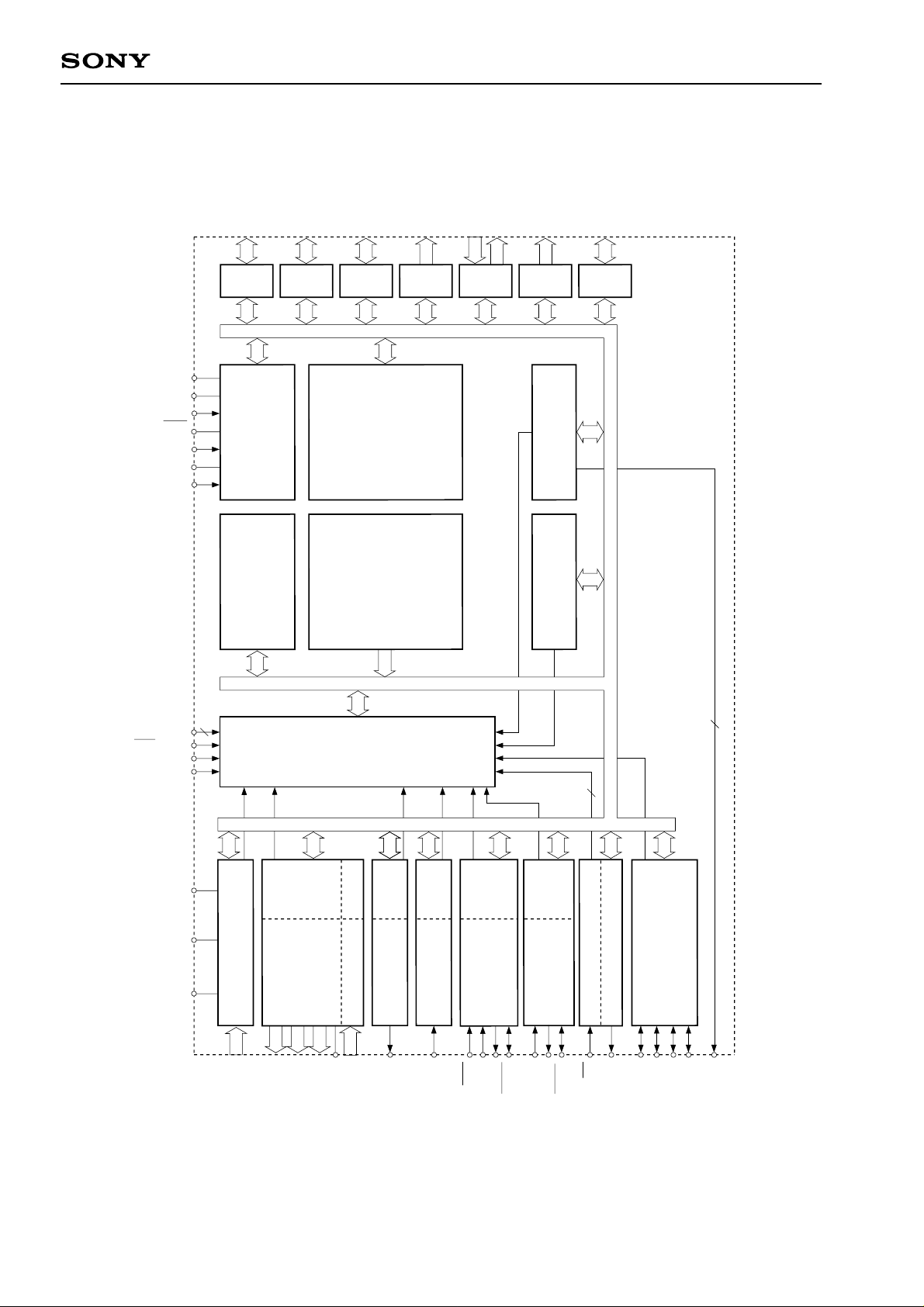
V
SS
V
DD
RST
XTAL
EXTAL
TX
TEX
PA0 to PA7
8
PB0 to PB7
8
PORT A
CLOCK
GENERATOR
SYSTEM CONTROL
SPC 700
CPU CORE
PORT B
PC0 to PC7
8
PD0 to PD7
8
PORT C
RAM
2048 BYTES
ROM
BYTES
40K/48K/52K/60K
PE0 to PE5
6
PORT D
PE6 to PE7
2
PF0 to PF3
4
PORT E
PG0 to PG3
4
PORT F
PORT G
32KHz
TIMER/COUNTER
PRESCALER/
TIME BASE TIMER
Block Diagram
INT3/NMI
INT2
INT1
INT0
AV
DD
REF
AV
AV
SS
2
A/D CONVERTER
8
AN0 to AN7
RAM
FDP
DRIVER
CONTROLLER/
8
8
12
FDP
V
T0 to T7
S0 to S11
T8/S19 to T15/S12
RAM
RAMKEY SCAN
BUFFER
REMOCON OUT
8
RMCO
KR0 to KR7
INTERRUPT CONTROLLER
FIFO
RAM
BUFFER
SERIAL
REMOCON IN
RMC
INTERFACE
SI0
CS0
SO0
UNIT (CH0)
SCK0
FIFO
SERIAL
UNIT (CH1)
INTERFACE
SI1
SO1
SCK1
2
C BUS
2
I
8 BIT TIMER 1
INTERFACE UNIT
8 BIT TIMER/COUNTER 0
TO
EC
SCL0
SCL1
SDA0
SDA1
ADJ
2
– 2 –
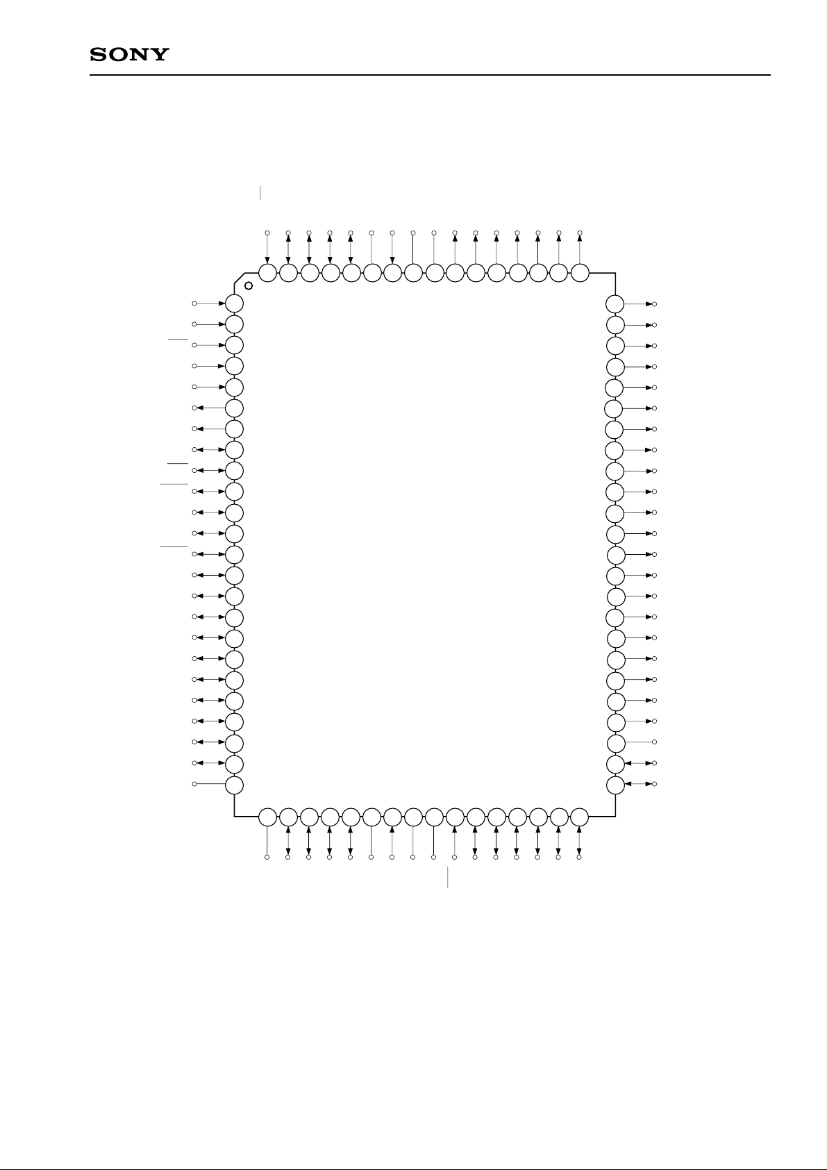
Pin Assignment (Top View)
CXP82940/82948/82952/82960
PE1/INT1
PE2/INT2
PE3/INT3/NMI
PE4/RMC
PE5
PE6/RMCO
PE7/TO/ADJ
PB0
PB1/CS0
PB2/SCK0
PB3/SI0
PB4/SO0
PB5/SCK1
PB6/SI1
PB7/SO1
PA0/AN0
PA1/AN1
PA2/AN2
PA3/AN3
PA4/AN4
PA5/AN5
PA6/AN6
PA7/AN7
DD
AV
10
11
12
13
14
15
16
17
18
19
20
21
22
23
24
1
2
3
4
5
6
7
8
9
PE0/EC/INT0
PG3
80
79
78
PG2
77
PG1
76
PG0
75
NC
74
TEX
73
TX
72
DD
V
71
T0
70
T1
69
T2
68
T3
67
T4
66
T5
65
T6
59
64
63
62
61
60
58
57
56
55
54
53
52
51
50
49
48
47
46
45
44
43
42
41
T7
T8/S19
T9/S18
T10/S17
T11/S16
T12/S15
T13/S14
T14/S13
T15/S12
S11
S10
S9
S8
PD7/S7
PD6/S6
PD5/S5
PD4/S4
PD3/S3
PD2/S2
PD1/S1
PD0/S0
FDP
V
PC7/KR7
PC6/KR6
25
REF
AV
26
27
PF0/SCL0
28
29
PF1/SCL1
PF2/SDA0
31
30
SS
AV
PF3/SDA1
32
XTAL
EXTAL
33
SS
V
34
35
RST
36
PC1/KR1
PC0/KR0
Note) NC (Pin 75) must be connected to VDD.
– 3 –
37
38
PC2/KR2
40
39
PC3/KR3
PC4/KR4
PC5/KR5
Pin Description
CXP82940/82948/82952/82960
Pin code
PA0/AN0
to
PA7/AN7
PB0
PB1/CS0
PB2/SCK0
PB3/SI0
PB4/SO0
PB5/SCK1
PB6/SI1
PB7/SO1
PC0/KR0
to
PC7/KR7
I/O
I/O/
Analog input
I/O
I/O/Input
I/O/I/O
I/O/Input
I/O/Output
I/O/I/O
I/O/Input
I/O/Output
I/O/Input
(Port A)
8-bit I/O port. I/O can
be set in a unit of
single bits.
Incorporation of pull-up
resistor can be set
through the software in
a unit of 4 bits.
(8 pins)
(Port B)
8-bit I/O port. I/O can
be set in a unit of
single bits.
Incorporation of pull-up
resistor can be set
through the software in
a unit of 4 bits.
(8 pins)
(Port C)
8-bit I/O port. I/O can
be set in a unit of single
bits. Capable of driving
12mA sync current.
Incorporation of pull-up
resistor can be set
through the software in
a unit of 4 bits.
(8 pins)
Functions
Analog inputs to A/D converter. (8 pins)
Chip select input for serial interface (CH0).
Serial clock I/O (CH0).
Serial data input (CH0).
Serial data output (CH0).
Serial clock I/O (CH1).
Serial data input (CH1).
Serial data output (CH1).
Serves as key return inputs when operating
key scan with fluorescent display panel (FDP)
segment signal (8 pins).
PE0/INT0/EC
PE1/INT1
PE2/INT2
PE3/INT3/
NMI
PE4/RMC
PE5
PE6/RMCO
PE7/TO/ADJ
PF0/SCL0
PF1/SCL1
PF2/SDA0
PF3/SDA1
Input/Input/Input
Input/Input
Input/Input
Input/Input/Input
Input/Input
Input
Output/Output
Output/Output/
Output
Output/I/O
Output/I/O
(Port E)
8-bit port. Lower 6 bits
are for inputs; upper
2 bits are for outputs.
(8 pins)
(Port F)
4-bit output port,
operating as N-ch open
drain output for large
current (12mA).
(4 pins)
External event inputs for
Inputs for
timer/counter.
external
interruption
request.
(4 pins)
Non-maskable interruption
request input.
Remote control reception circuit input.
Carrier output of remote control transmission
circuit.
Output for the timer/counter rectangular waves,
and 32kHz oscillation dividing frequency.
Transfer clock I/Os for I2C bus interface.
Transfer data I/Os for I2C bus interface.
– 4 –
Pin code I/O Functions
(Port G)
8-bit I/O port. I/O can be set in a unit of single bits.
I/OPG0 to PG3
Incorporation of pull-up resistor can be set through the software in a unit
of 4 bits.
(4 pins)
CXP82940/82948/82952/82960
PD0/S0
to
PD7/S7
T8/S12
to
T15/S19
T0 to T7
VFDP
EXTAL
XTAL
TEX
TX
RST
NC
AVDD
AVREF
(Port D)
Output/Output
8-bit output ports.
(8 pins)
OutputS8 to S11 FDP segment signal outputs. (4 pins)
Output/Output
Output
Outputs for FDP timing signals/segment signals.
(8 pins)
FDP timing signal outputs.
FDP voltage supply when incorporated resistor is set by mask option.
Input
Crystal connectors for system clock oscillation. When the clock is
supplied externally, input to EXTAL; opposite phase clock should be
Output
Input
input to XTAL.
Crystal connectors for 32kHz timer/counter clock oscillation. Set 32kHz
crystal oscillator between TEX and TX. For usage as event input, attach
Output
Input
clock source to TEX, and open TX.
Low-level active, system reset.
NC. Under normal operation, connect to VDD.
Positive power supply for A/D converter.
Input
Reference voltage input for A/D converter.
FDP segment signal outputs.
(8 pins)
AVSS
VDD
VSS
A/D converter GND.
Positive power supply.
GND.
– 5 –

Data bus
RD (Port B)
Port B direction
IP
Port B data
Pull-up resistor
"0" when reset
"0" when reset
∗
Pull-up transistor approx. 100kΩ
∗
Schmitt input
CS0
SI0
SI1
Not Schmitt input for SI0 and SI1.
Data bus
RD (Port B)
IP
Port B output
selection
"0" when reset
∗
Pull-up transistor approx. 100kΩ
∗
Schmitt input
SCK in
Port B data
Port B direction
"0" when reset
Pull-up resistor
"0" when reset
SCK OUT
Output enable
A
I/O Circuit Format for Pins
CXP82940/82948/82952/82960
Pin
PA0/AN0
to
PA7/AN7
8 pins
Port A
Port B
Data bus
Pull-up resistor
"0" when reset
Port A data
Port A direction
"0" when reset
RD (Port A)
Port A input
selection
AA
"0" when reset
Circuit format
A/D converter
∗
Input
IP
protection
circuit
Input multiplexer
∗
Pull-up transistor approx. 100kΩ
When reset
Hi-Z
PB1/CS0
PB3/SI0
PB6/SI1
3 pins
PB2/SCK0
PB5/SCK1
2 pins
Port B
– 6 –
Hi-Z
Hi-Z
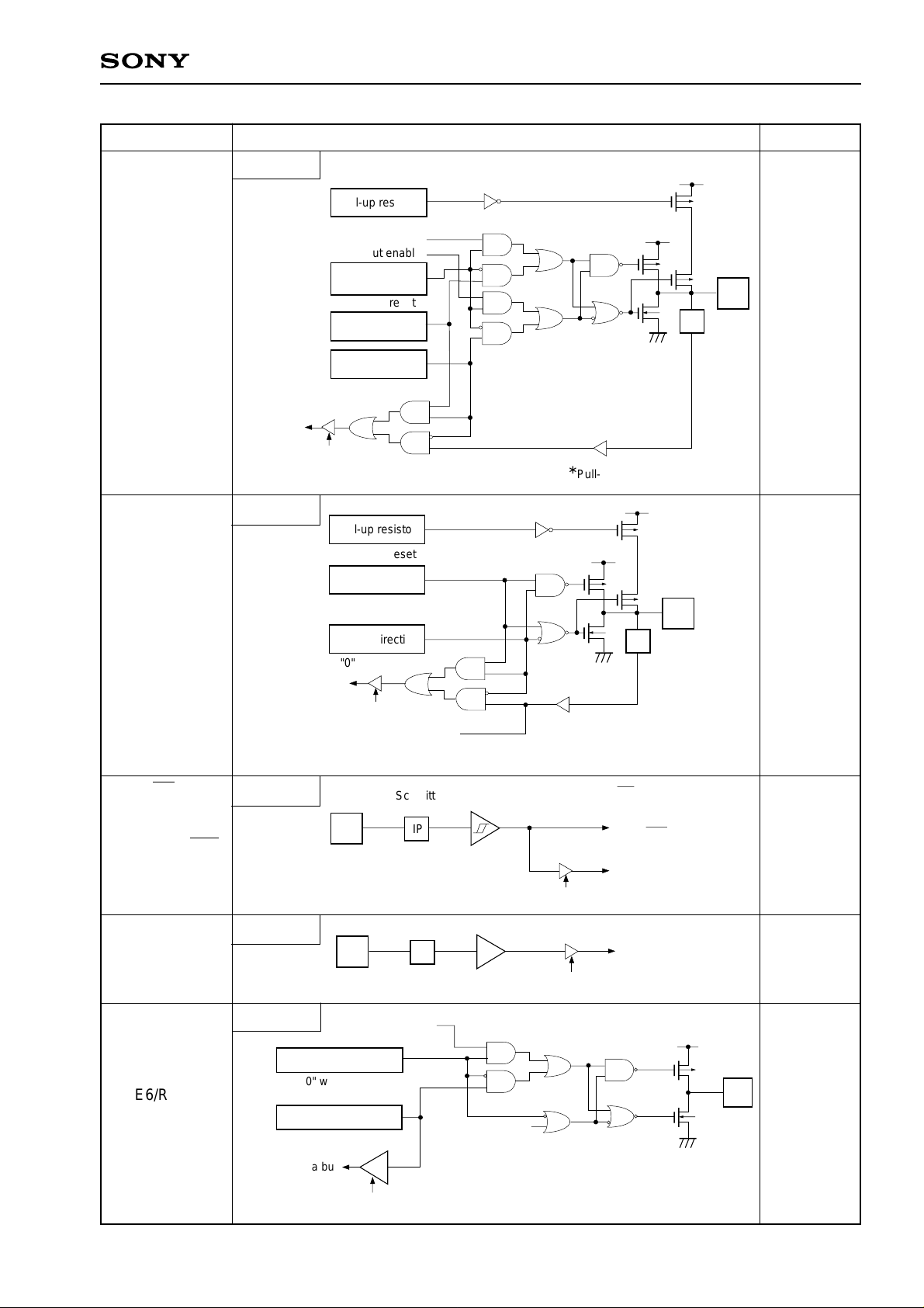
CXP82940/82948/82952/82960
PB4/SO0
PB7/SO1
2 pins
PC0/KR0
to
PC7/KR7
Port B
Data bus
Port C
Pull-up resistor
"0" when reset
"0" when reset
Port B direction
“0” when reset
RD (Port B)
Pull-up resistor
"0" when reset
Port C direction
"0" when reset
Data bus
Output enable
Port B output
selection
Port B data
Port C data
SO
Circuit format
∗
IP
∗
Pull-up transistor approx. 100kΩ
∗
2
∗1
IP
When resetPin
Hi-Z
Hi-Z
8 pins
PE0/EC/INT0
PE1/INT1
PE2/INT2
PE3/INT3/NMI
PE4/RMC
5 pins
PE5
1 pin
PE6/RMCO
Port E
Port E
Port E
Port E output selection
"0" when reset
Reset E data
"1" when reset
RD (Port C)
Key input signal
Schmitt input
IP
IP
Remote control
transmission circuit
Output enable
∗
1
Large current 12mA
∗
2
Pull-up transistor approx. 100kΩ
EC/INT0
INT1
INT2
INT3/NMI
RMC
Data bus
RD (Port E)
Data bus
RD (Port E)
Hi-Z
Hi-Z
High level
1 pin
Data bus
RD (Port E)
– 7 –
CXP82940/82948/82952/82960
PE7/TO/ADJ
1 pin
PF0/SCL0
PF1/SCL1
PF2/SDA0
PF3/SDA1
4 pins
Port E
Port E data
"1" when reset
ADJ16K
ADJ2K
Port E output selection (upper)
Port E output selection (lower)
"00" when reset
00
01
TO
∗
1
10
∗
1
11
TO output enable
Port F
SCL, SDA
2
I
C output enable
("0" when reset)
Port F data
"1" when reset
SCL, SDA
(I2C circuit)
Circuit format
Internal reset signal
MPX
Schmitt input
∗
2
∗
1
ADJ signal is a frequency dividing output for
32kHz oscillation frequency adjustment.
ADJ2 can be used for buzzer output.
∗
2
Pull-up transistor approx. 150k Ω.
Large current
12mA
IP
BUS SW
To internal I2C pin
(to SCL1 for SCL0)
When resetPin
High level
(
with approx.
150kΩ
resistor when
reset)
Hi-Z
PB0
PG0 to PG3
5 pins
Port B
Port G
Port B data or
Port G data
Port B direction or
Port G direction
"0" when reset
Data bus
RD (Port B or Port G)
Pull-up resistor
"0" when reset
∗
IP
∗
Pull-up transistor approx. 100kΩ
Hi-Z
– 8 –
 Loading...