

Sony CXP824P40A Datasheet

CXP824P40A
CMOS 8-bit Single Chip Microcomputer
Description
The CXP824P40A is a CMOS 8-bit single chip
microcomputer integrating on a single chip an A/D
converter, serial interface, timer/counter, time base
timer, capture timer counter, fluorescent display tube,
controller/driver, remote control reception circuit, CTL
duty detection circuit, 14-bit PWM output and highspeed output circuit besides the basic configurations
of 8-bit CPU, PROM, RAM, and I/O port.
The CXP824P40A also provides sleep/stop function
that enables lower power consumption.
CXP824P40A is the PROM-incorporated version of
the CXP82440A with built-in mask ROM. This
provides the additional feature of being able to write
directly into the program. Thus, it is most suitable for
evaluation use during system development and for
small-quantity production.
Structure
Silicon gate CMOS IC
100 pin QFP (Plastic)
Features
• Wide-range instruction system (213 instructions) to cover various types of data
— 16-bit arithmetic/multiplication and division/boolean bit operation instructions
• Minimum instruction cycle 400ns at 10MHz operation
122µs at 32kHz operation
• Incorporated PROM capacity 40K bytes
• Incorporated RAM capacity 1120 bytes (including fluorescent display area)
• Peripheral functions
— A/D converter 8-bit, 8-channel, successive approximation method
(Conversion time of 32µs/10MHz)
— Serial interface Incorporated 8-bit, 8-stage FIFO
(Auto transfer for 1 to 8 bytes), 1 channel
8-bit clock sync type, 1 channel
— Timers 8-bit timer, 8-bit timer/counter, 19-bit time base timer
16-bit capture timer/counter, 32kHz timer/counter
— Fluorescent display tube controller/driver Maximum of 384 segments display possible
1 to 16-digit dynamic display
Dimmer function
High voltage drive output (40V)
On-chip pull-down resistor (Mask option)
Hardware key scan function
(Maximum of 16 × 8 key matrix compatible)
— Remote control receiving circuit Incorporated noise elimination circuit
8-bit measurement counter with on-chip 6-stage FIFO
— PWM output 14 bits, 1 channel
— CTL duty detection circuit
— High-speed output circuit RTG 4 pins
• Interruption 19 factors, 15 vectors, multi-interruption possible
• Standby mode SLEEP/STOP
• Package 100-pin plastic QFP
Sony reserves the right to change products and specifications without prior notice. This information does not convey any license by
any implication or otherwise under any patents or other right. Application circuits shown, if any, are typical examples illustrating the
operation of the devices. Sony cannot assume responsibility for any problems arising out of the use of these circuits.
– 1 –
E94Z17-PP
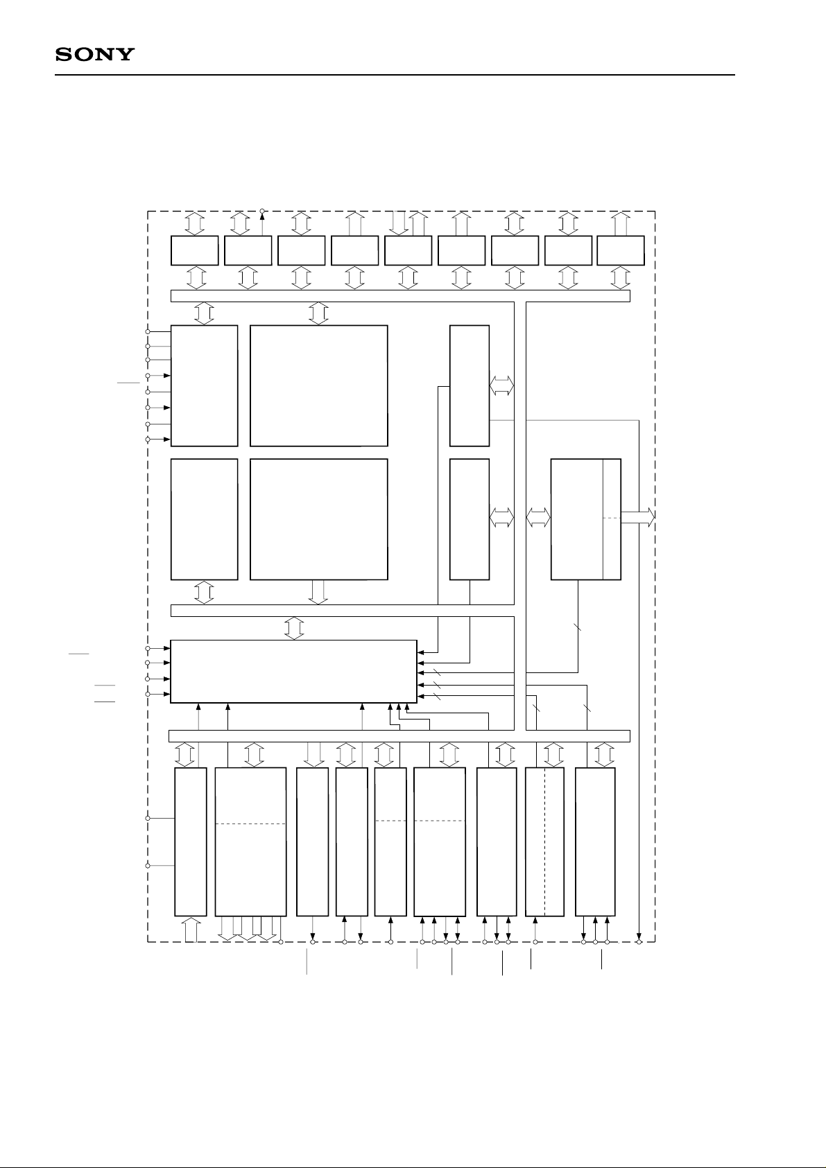
CXP824P40A
V
SS
Vpp
V
DD
RST
XTAL
EXTAL
TX
TEX
PB0 to PB6
PA0 to PA7
8
PORT A
PB7
7
PORT B
CLOCK GEN./
SYSTEM CONTROL
SPC 700
CPU CORE
PC0 to PC7
8
PORT C
RAM
1120 BYTES
PROM
40K BYTES
PD0 to PD7
8
PE0 to PE5
6
PORT D
PE6 to PE7
2
PF0 to PF7
8
PORT E
32kHz
PRESCALER/
PG0 to PG7
8
PORT F
PORT G
TIMER/COUNTER
TIME BASE TIMER
PH0 to PH7
8
PORT H
PULSE
REALTIME
GENERATOR
PI0 to PI7
8
PORT I
4
CH0 CH1
PG3/RTO3
PG0/RTO0 to
PE3/INT3/NMI
PE2/INT2
PE1/EC1/INT1
PE0/EC0/INT0
AV
REF
AV
SS
RAM
A/D CONVERTER
FDP
CONTROLLER/
8
8
PA7/AN7
8
T0 to T7
PA0/AN0 to
T15/S24 to T8/S31
DRIVER
14 BIT PWM GENERATOR
24
FDP
V
PE6/PWM
PD0/S0 to PI7/S23
INTERRUPT CONTROLLER
2
2 2
FIFOREMOCON
CTL DUTY DET
FIFO
UNIT 0
SERIAL
INTERFACE
PE5/CTL
PE7/DDO
PE4/RMC
PB3/SI0
PB1/CS0
PB4/SO0
PB2/SCK0
2
2
8 BIT TIMER/COUNTER 0
SERIAL INTERFACE UNIT 1
PB6/SI1
PB7/SO1
PB5/SCK1
2
8 BIT TIMER 1
16 BIT CAPTURE
TIMER/COUNTER 2
PE7/TO
PB0/CINT
PE0/INT0/EC0
PE7/ADJ
PE1/INT2/EC1
Block Diagram
– 2 –
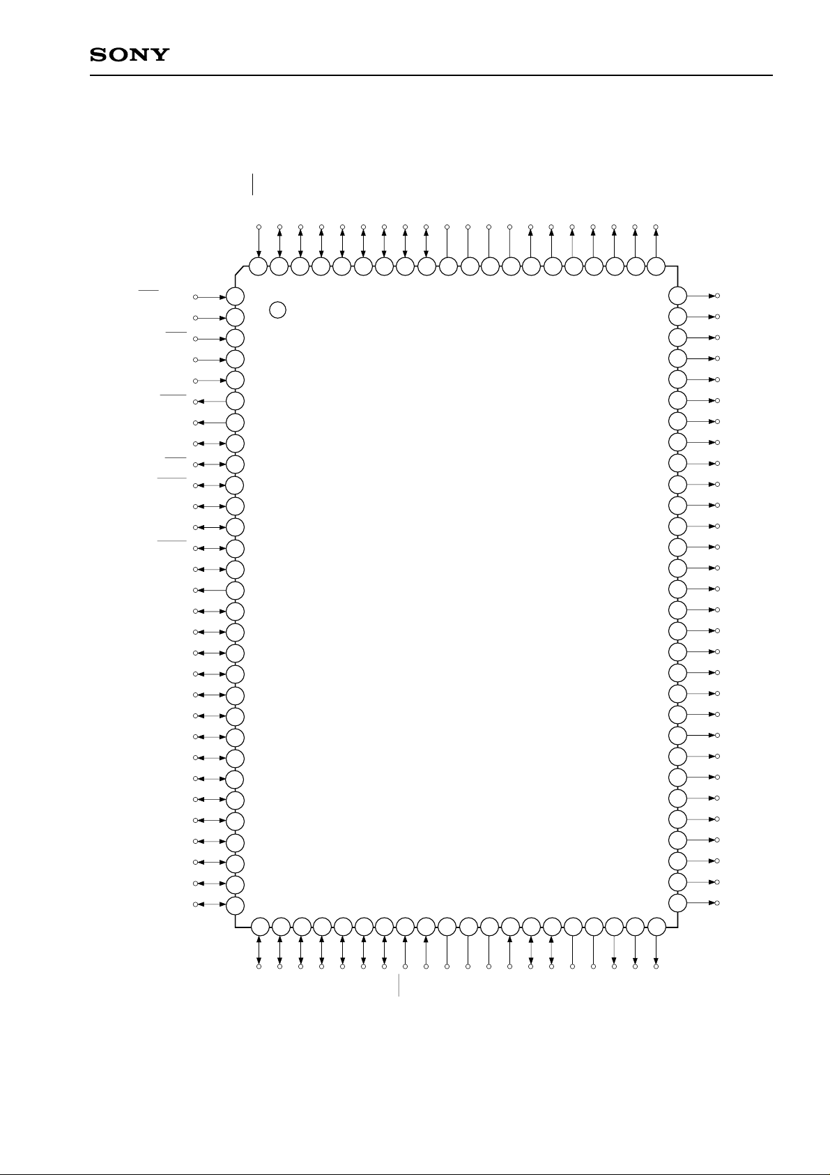
Pin Assignment (Top View)
100
PG6
PG7
PE0/EC0/INT0
99
98
97
PG5
96
PG3/RTO3
PG4
95
PG1/RTO1
PG2/RTO2
93
94
Vss
PG0/RTO0
92
91
90
Vpp
89
DD
V
88
FDP
V
87
T0
86
T1
85
T2
84
T3
83
T4
82
T5
CXP824P40A
T6
81
PE1/EC1/INT1
PE2/INT2
PE3/INT3/NMI
PE4/RMC
PE5/CTL
PE6/PWM
PE7/TO/DDO/ADJ
PB0/CINT
PB1/CS0
PB2/SCK0
PB3/SI0
PB4/SO0
PB5/SCK1
PB6/SI1
PB7/SO1
PC0/KR0
PC1/KR1
PC2/KR2
PC3/KR3
PC4/KR4
PC5/KR5
PC6/KR6
PC7/KR7
PH0
PH1
PH2
PH3
PH4
PH5
PH6
10
11
12
13
14
15
16
17
18
19
20
21
22
23
24
25
26
27
28
29
30
49
50
80
75
74
73
72
65
62
61
79
78
77
76
71
70
69
68
67
66
64
63
60
59
58
57
56
55
54
53
52
51
T7
T8/S31
T9/S30
T10/S29
T11/S28
T12/S27
T13/S26
T14/S25
T15/S24
PI7/S23
PI6/S22
PI5/S21
PI4/S20
PI3/S19
PI2/S18
PI1/S17
PI0/S16
PF7/S15
PF6/S14
PF5/S13
PF4/S12
PF3/S11
PF2/S10
PF1/S9
PF0/S8
PD7/S7
PD6/S6
PD5/S5
PD4/S4
PD3/S3
1
2
3
4
5
6
7
8
9
35
31
32
33
34
36
37
38
39
40
41
42
43
44
45
46
47
48
PH7
PA1/AN1
PA0/AN0
PA3/AN3
PA2/AN2
PA5/AN5
PA4/AN4
RST
XTAL
EXTAL
Vss
TEX
PA6/AN6
TX
Note) 1. Vpp (Pin 90) must be connected to VDD.
2. Vss (Pins 41 and 91) are both connected to GND.
– 3 –
REF
AV
PA7/AN7
AVss
PD1/S1
PD0/S0
PD2/S2

Pin Description
Pin code I/O Functions
(Port A)
PA0/AN0
to
PA7/AN7
I/O/
Analog input
8-bit I/O port. I/O can
be set in single bit
units.
Analog inputs to A/D converter. (8 pins)
(8 pins)
CXP824P40A
PB0/CINT
PB1/CS0
PB2/SCK0
PB3/SI0
PB4/SO0
PB5/SCK1
PB6/SI1
PB7/SO1
PC0/KR0
to
PC7/KR7
PD0/S0
to
PD7/S7
PE0/INT0/
EC0
PE1/INT1/
EC1
PE2/INT2
PE3/INT3/
NMI
PE4/RMC
PE5/CTL
I/O/Input
I/O/Input
I/O/I/O
I/O/Input
I/O/Output
I/O/I/O
I/O/Input
Output/Output
I/O/Input
Output/Output
Input/Input/Input
Input/Input/Input
Input/Input
Input/Input/Input
Input/Input
Input/Input
(Port B)
8-bit I/O port. I/O for
lower 7 bits can be set
in a unit of single bits.
Uppermost bit (PB7) is
for output only.
(8 pins)
(Port C)
8-bit I/O port. I/O can
be set in a unit of single
bits. Capable of driving
12mA sync current.
(8 pins)
(Port D)
8-bit output port.
(8 pins)
(Port E)
8-bit port. Lower 6 bits
are for inputs; upper
2 bits are for outputs.
(8 pins)
Capture input to 16-bit timer/counter.
Chip select input for serial interface (CH0).
Serial clock I/O (CH0).
Serial data input (CH0).
Serial data output (CH0).
Serial clock I/O (CH1).
Serial data input (CH1).
Serial data output (CH1).
Serves as key return inputs when operating
key scan with FDP segment signal.
FDP segment signal outputs.
External event inputs for
Inputs for
external
timer/counter.
(2 pins)
interruption
request.
(4 pins)
Non-maskable interruption
request input.
Remote control reception circuit input.
Input for CTL duty direction circuit.
PE6/PWM
PE7/TO/
DDO/ADJ
PF0/S8
to
PF7/S15
PG0/RTO0
to
PG3/RTO3
PG4 to PG7
Output/Output
Output/Output/
Output/Output
Output/Output
I/O/Output
I/O
14-bit PWM output.
Output for the 16-bit timer/counter rectangular
waves, CTU duty detection, and 32kHz
oscillation frequency demultiplication.
(Port F)
8-bit output port.
FDP segment signal outputs.
(8 pins)
(Port G)
8-bit I/O port. I/O can
be set in a unit of single
bits. Data for the lower
Outputs for real-time pulse generator (RTG).
Functions as high-precision, real-time pulse
output port.
(4 pins)
4 bits are gated with the
contents of RTO or OR-gate output. (8 pins)
– 4 –
Pin code I/O Functions
(Port H)
I/OPH0 to PH7
8-bit I/O port. I/O can be set in a unit of single bits.
(8 pins)
CXP824P40A
PI0/S16
to
PI7/S23
T8/S31
to
T15/S24
T0 to T7
VFDP
EXTAL
XTAL
TEX
TX
RST
AVREF
AVSS
VDD
Vpp
Output/Output
Output/Output
Output
Input
Output
Input
Output
Input
Input
(Port I)
8-bit output ports.
FDP segment signal outputs.
(8 pins)
Outputs for FDP timing (digit) signals/segment signals.
FDP timing signal outputs.
FDP voltage supply when incorporated resistor is set by mask option.
Crystal connectors system clock oscillation. When the clock is supplied
externally, input to EXTAL; opposite phase clock should be input to
XTAL.
Crystal connectors for 32kHz timer/counter clock oscillation. Set 32kHz
crystal oscillator between TEX and TX. For usage as event input, attach
clock source to TEX, and open TX.
Low-level active, system reset.
Reference voltage input for A/D converter.
A/D converter GND.
Vcc supply.
VCC supply for incorporated PROM writing.
Connect to VDD during normal operation.
VSS
GND.
– 5 –
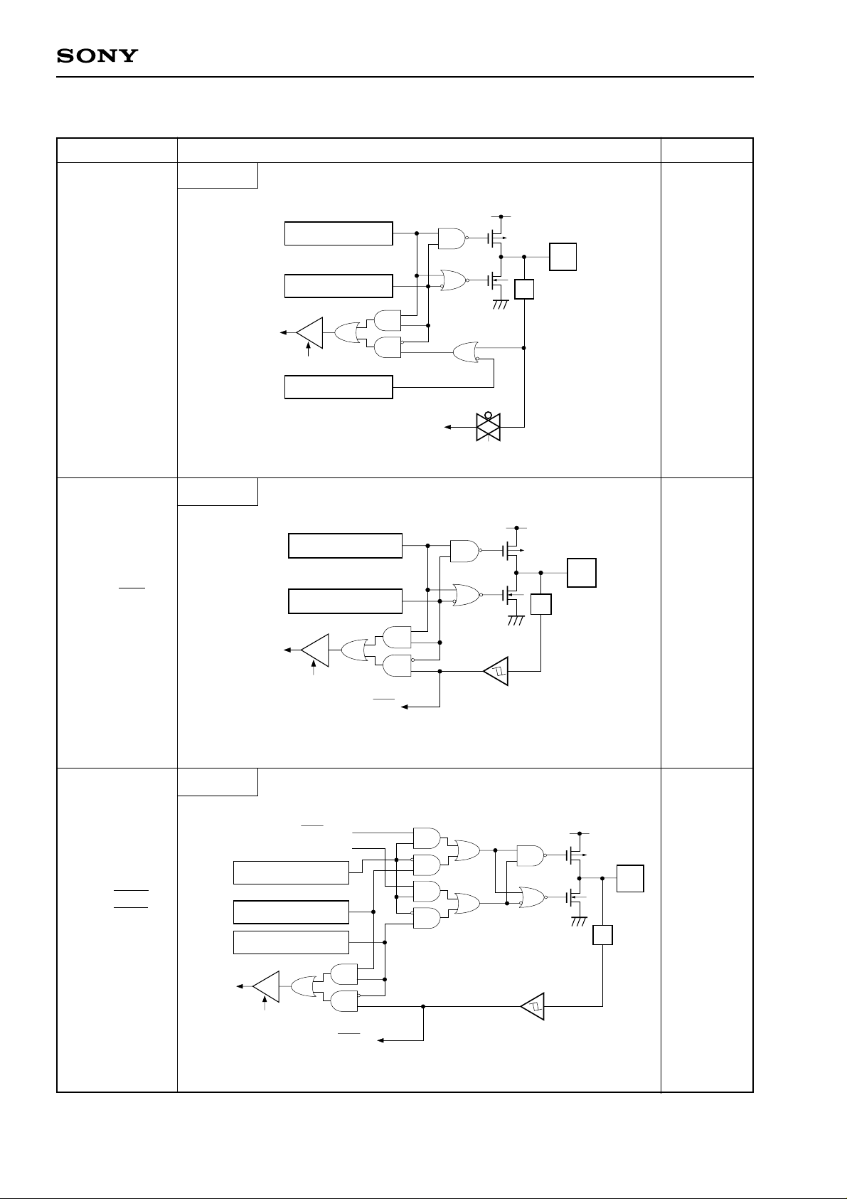
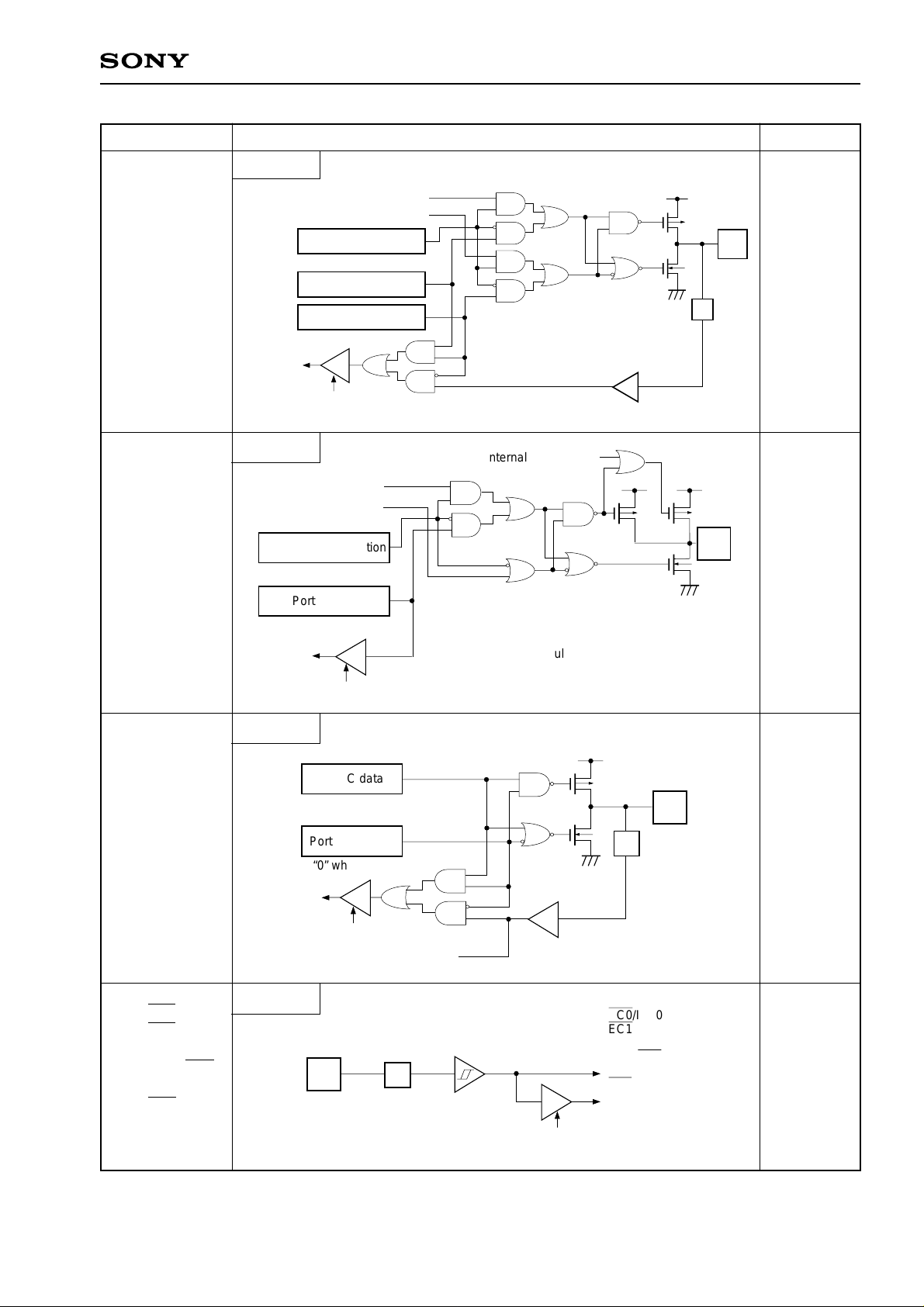
I/O Circuit Format for Pins
CXP824P40A
Pin
PA0/AN0
to
PA7/AN7
8 pins
Port A
Port B
Data bus
Circuit format
Port A data
Port A direction
“0” when reset
RD (Port A)
Port A input selection
“0” when reset
A/D converter
Port B data
Input protection circuit
Input multiplexer
IP
When reset
Hi-Z
PB0/CINT
PB1/CS0
PB3/SI0
PB6/SI1
4 pins
PB2/SCK0
PB5/SCK1
Port B
Data bus
Port B direction
“0” when reset
Data bus
RD (Port B)
SCK OUT
Output enable
Port B output selection
“0” when reset
Port B data
Port B direction
“0” when reset
CINT
CS0
SI0
SI1
Schmitt input
Schmitt input
IP
Hi-Z
IP
Hi-Z
2 pins
RD (Port B)
SCK in
– 6 –
CXP824P40A
Pin
PB4/SO0
1 pin
PB7/SO1
Port B
Ouput enable
Port B output selection
“0” when reset
Port B data
Port B direction
“0” when reset
Data bus
RD (Port B)
Port B
Output enable
Port B output selection
“1” when reset
SO
SO
Circuit format
Internal reset signal
When reset
Hi-Z
IP
∗
High level
1 pin
PC0/KR0
to
PC7/KR7
8 pins
PE0/EC0/INT0
PE1/EC1/INT1
PE2/INT2
PE3/INT3/NMI
PE4/RMC
PE4/CTL
“1” when reset
Data bus
Port C
Data bus
Port E
Port B data
RD (Port B)
Port C data
Port C direction
“0” when reset
RD (Port C)
Key input signal
Schmitt input
IP
∗
Pull-up transistor approx.
200kΩ
∗
IP
∗
High current drive of 12mA possible
EC0/INT0
EC1/INT1
INT2
INT3/NMI
RMC
CTL
Data bus
Hi-Z
Hi-Z
6 pins
RD (Port E)
– 7 –
 Loading...