

Sony CXP81960, CXP81952 Datasheet

CXP81952/81960
CMOS 8-bit Single Chip Microcomputer
Description
The CXP81952/81960 is a CMOS 8-bit microcomputer which consists of A/D converter, serial
interface, timer/counter, time base timer, vector
interruption, high precision timing pattern generation
circuit, PWM generator, PWM for tuner, 32kHz
timer/event counter, remote control receiving circuit,
general purpose prescaler, and external signal, as
well as basic configurations like 8-bit CPU, ROM,
RAM and I/O port. They are integrated into a single
chip.
Also the CXP81952/81960 provides sleep/stop
function which enables to lower power consumption
and ultra-low speed instruction mode in 32kHz
operation.
100 pin QFP (PIastic) 100 pin LQFP (PIastic)
Structure
Silicon gate CMOS IC
Features
• A wide instruction set (213 instructions) which cover various types of data
— 16-bit operation/multiplication and division/boolean bit operation instructions
• Minimum instruction cycle 250ns at 16MHz operation
122µs at 32kHz operation
• Incorporated ROM capacity 52K bytes (CXP81952), 60K bytes (CXP81960)
• Incorporated RAM capacity 2048 bytes
• Peripheral functions
— A/D converter 8-bit, 12-channel, successive approximation system
(Conversion time 20.0µs/16MHz)
— Serial Interface Incorporated buffer RAM (1 to 32 bytes auto transfer) 1-channel
Incorporated 8-bit and 8-stage FIFO for data
(1 to 8 bytes auto transfer) 1-channel
— Timer 8-bit timer, 8-bit timer/counter, 19-bit time base timer,
32kHz timer/counter
— High precision timing pattern generator PPG 19-pin 32-stage programmable
RTG 5-pin 2-channel
— PWM/DA gate output PWM 12-bit, 2-channel (Repetitive frequency 62kHz/16MHz)
DA gate pulse output 13-bit, 4-channel
— FRC capture unit Incorporated 26-bit and 8-stage FIFO
— PWM output 14-bit, 1-channel
— Remote control receiving circuit 8-bit pulse measurement counter with on-chip, 6-stage FIFO
— General purpose prescaler 7-bit (PG5 input frequency divided, FRC capture possible)
• Interruption 20 factors, 15 vectors, multi-interruption possible
• Standby mode SLEEP/STOP
• Package 100-pin plastic QFP/LQFP
• Piggyback/evaluation chip CXP81900 100-pin ceramic QFP/LQFP
Sony reserves the right to change products and specifications without prior notice. This information does not convey any license by
any implication or otherwise under any patents or other right. Application circuits shown, if any, are typical examples illustrating the
operation of the devices. Sony cannot assume responsibility for any problems arising out of the use of these circuits.
– 1 –
E95110-ST
CXP81952/81960
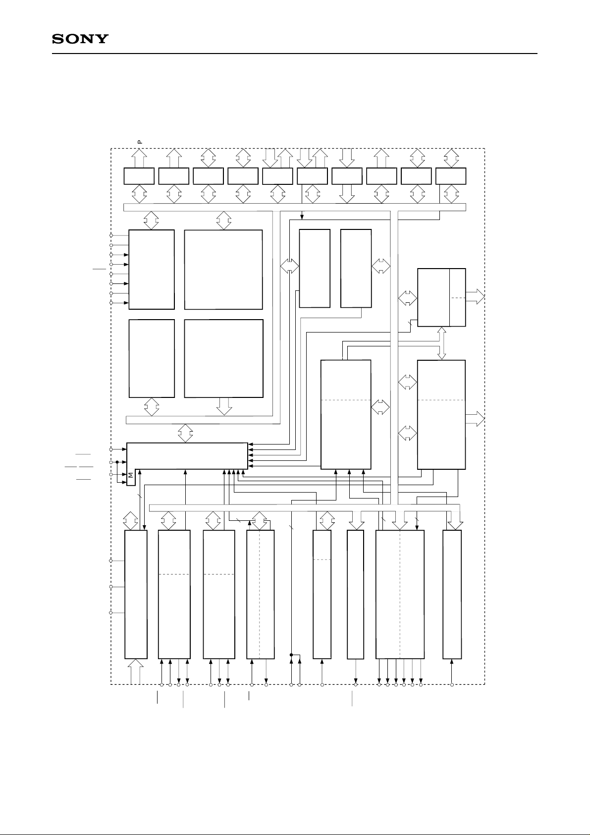
Vss
V
DD
MP
RST
XTAL
EXTAL
TX
TEX
PE1/INT2
PI4/INT1/NMI
PE0/INT0
PA0 to PA7
8
PORT A
CLOCK
GENERATOR/
SYSTEM CONTROL
SPC700
CPU CORE
NMI
2
PB0 to PB7
PC0 to PC7
8
PORT B8PORT C
PD0 to PD7
PE0 to PE1
PE2 to PE7
2
8
PORT D
6
PORT E
RAM
2048 BYTES
ROM
52K/60K BYTES
INTERRUPT CONTROLLER
PF4 to PF7
PF0 to PF3
4
PG0 to PG7
PH0 to PH7
4
PORT F8PORT G8PORT H7PORT I
32kHz
PRESCALER/
TIME BASE TIMER
TIMER/COUNTER
FIFO
FRC
CAPTURE UNIT
PI1 to PI7
REALTIME
2
PJ0 to PJ7
8
PORT J
1
CH
5
PULSE
CH0
GENERATOR
RAM
19
PATTERN
GENERATOR
PROGRAMMABLE
PC7/RTO7
to
PC3/RTO3
PC2/PPO18
to
PA0/PPO0
AVss
AV
REF
AV
DD
Block Diagram
A/D CONVERTER
12
PF0/AN4
PF7/AN11
AN0 to AN3
to
RAM
(CH0)
SERIAL
INTERFACE UNIT
SI0
CS0
SO0
SCK0
2
FIFO
(CH1)
SERIAL
INTERFACE UNIT
PI7/SI1
PI6/SO1
PI5/SCK1
2
FIFO
8 BIT TIMER 1
8 BIT TIMER/COUNTER 0
PI3/TO
PE1/EC
PG6/EXI0
REMOCON INPUT
PI1/RMC
PG7/EXI1
– 2 –
2
14 BIT PWM GENERATOR
PI2/PWM
12 BIT PWM GENERATOR CH0
PE4/DAA0
PE2/PWM0
4
12 BIT PWM GENERATOR CH1
PE7/DAB1
PE5/DAA1
PE6/DAB0
PE3/PWM1
PROGRAMMABLE PRESCALER
PG5/PCK
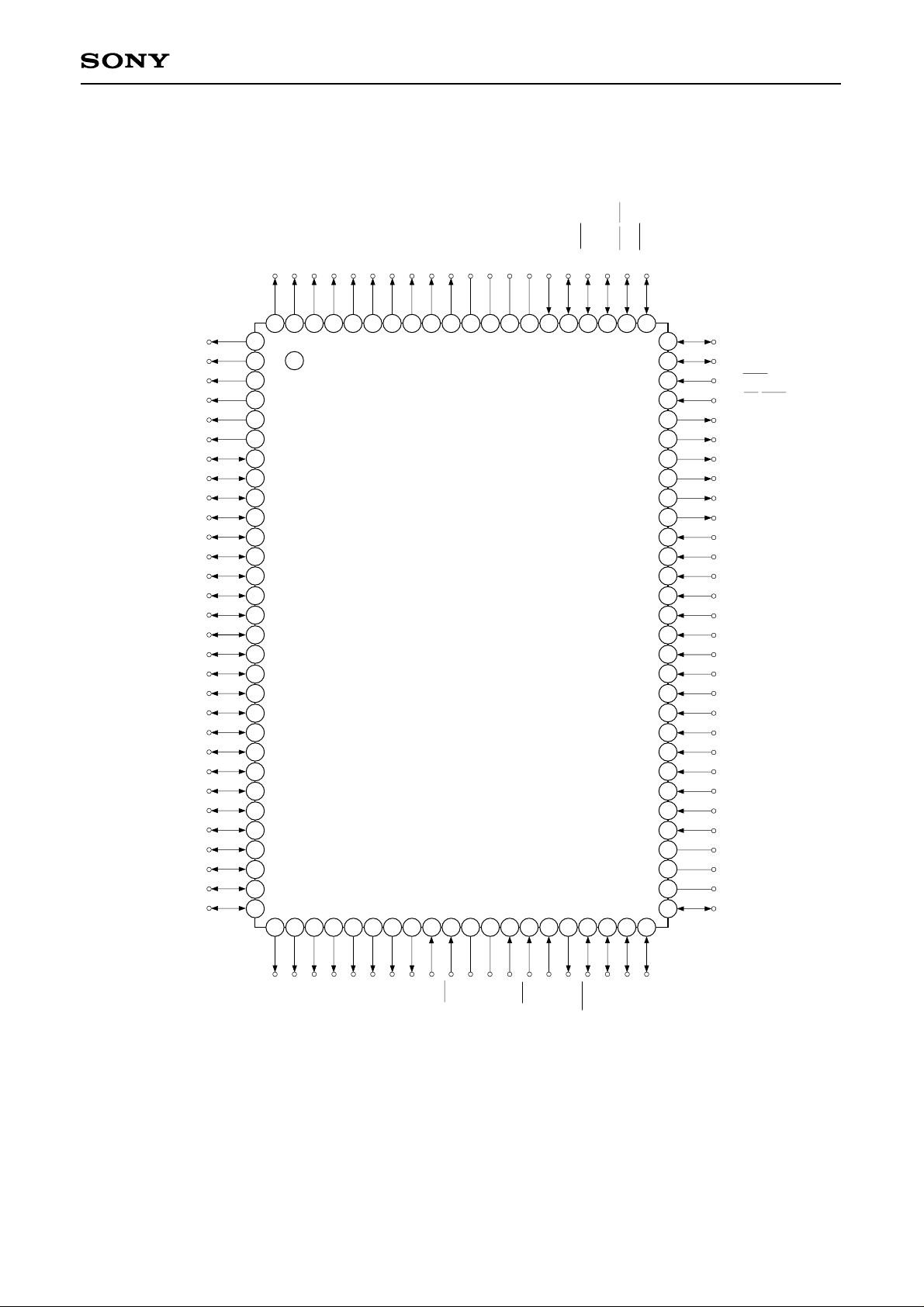
Pin Configuration 1 (Top View) 100-pin QFP package
PA6/PPO6
PA5/PPO5
PA4/PPO4
PA3/PPO3
PA2/PPO2
PA1/PPO1
PA0/PPO0
PB7/PPO15
PB6/PPO14
DD
V
NC
PA7/PPO7
CXP81952/81960
SS
TX
V
TEX
PI2/PWM
PI1/RMC
PI5/SCK1
PI4/INT1/NMI
PI3/TO/ADJ
PB5/PPO13
PB4/PPO12
PB3/PPO11
PB2/PPO10
PB1/PPO9
PB0/PPO8
PC7/RTO7
PC6/RTO6
PC5/RTO5
PC4/RTO4
PC3/RTO3
PC2/PPO18
PC1/PPO17
PC0/PPO16
PJ7
PJ6
PJ5
PJ4
PJ3
PJ2
PJ1
PJ0
PD7
PD6
PD5
PD4
PD3
PD2
PD1
PD0
10
12
13
14
15
16
17
19
29
30
11
18
20
21
22
23
24
25
26
27
28
100
99
98
1
2
3
4
5
6
7
8
9
32
31
33
97
34
96
35
95
36
94
37
93
38
92
39
91
40
90
41
89
42
88
43
87
44
86
45
85
46
84
47
83
48
82
49
81
50
80
79
78
77
76
75
71
69
68
67
66
65
64
63
62
60
59
58
57
74
73
72
70
61
56
55
54
53
52
51
PI6/SO1
PI7/SI1
PE0/INT0
PE1/EC/INT2
PE2/PWM0
PE3/PWM1
PE4/DAA0
PE5/DAA1
PE6/DAB0
PE7/DAB1
PG0
PG1
PG2
PG3
PG4
PG5/PCK
PG6/EXI0
PG7/EXI1
AN0
AN1
AN2
AN3
PF0/AN4
PF1/AN5
PF2/AN6
PF3/AN7
AV
DD
AVREF
AVSS
PF4/AN8
PH7
PH6
PH5
PH4
PH3
PH2
PH1
PH0
MP
RST
SS
V
XTAL
CS0
EXTAL
SI0
SO0
Note) 1. NC (Pin 90) is always connected to VDD.
2. Vss (Pins 41 and 88) are both connected to GND.
– 3 –
SCK0
PF7/AN11
PF5/AN9
PF6/AN10
Pin Configuration 2 (Top View) 100-pin LQFP package
PA7/PPO7
PA6/PPO6
PA5/PPO5
PA4/PPO4
PA3/PPO3
PA2/PPO2
PA1/PPO1
PA0/PPO0
PB7/PPO15
PB6/PPO14
PB5/PPO13
PB4/PPO12
NC
CXP81952/81960
SS
DD
V
TX
V
TEX
PI2/PWM
PI1/RMC
PI5/SCK1
PI4/INT1/NMI
PI3/TO/ADJ
PI7/SI1
PI6/SO1
PE0/INT0
PB3/PPO11
PB2/PPO10
PB1/PPO9
PB0/PPO8
PC7/RTO7
PC6/RTO6
PC5/RTO5
PC4/RTO4
PC3/RTO3
PC2/PPO18
PC1/PPO17
PC0/PPO16
PJ7
PJ6
PJ5
PJ4
PJ3
PJ2
PJ1
PJ0
PD7
PD6
PD5
PD4
PD3
10
11
12
13
14
15
16
17
18
19
21
22
25
20
23
24
100
99
98
1
2
3
4
5
6
7
8
9
27
28
26
97
29
96
30
95
31
94
32
93
33
92
34
91
35
90
36
89
37
88
38
87
39
86
40
85
41
84
42
83
43
82
44
81
45
80
46
79
47
78
48
77
49
76
50
69
67
65
64
63
62
61
56
55
53
52
51
75
74
73
72
71
70
68
66
60
59
58
57
54
PE1/EC/INT2
PE2/PWM0
PE3/PWM1
PE4/DAA0
PE5/DAA1
PE6/DAB0
PE7/DAB1
PG0
PG1
PG2
PG3
PG4
PG5/PCK
PG6/EXI0
PG7/EXI1
AN0
AN1
AN2
AN3
PF0/AN4
PF1/AN5
PF2/AN6
PF3/AN7
AVDD
AVREF
SS
MP
PD2
PD1
PD0
PH7
PH6
PH5
PH4
PH3
PH2
PH1
PH0
RST
V
XTAL
EXTAL
Note) 1. NC (Pin 88) is always connected to VDD.
2. Vss (Pins 39 and 86) are both connected to GND.
– 4 –
CS0
SI0
SO0
SCK0
PF7/AN11
PF5/AN9
PF6/AN10
SS
AV
PF4/AN8
Pin Description
Symbol I/O Description
(Port A)
PA0/PPO0
to
PA7/PPO7
Output/
Real time
output
8-bit output port. Data is
gated with PPO contents by
OR-gate and they are output.
(8 pins)
(Port B)
PB0/PPO8
to
PB7/PPO15
Output/
Real time
output
8-bit output port. Data is
gated with PPO contents by
OR-gate and they are output.
(8 pins)
CXP81952/81960
Programmable pattern generator (PPG)
output.
Functions as high precision real time
pulse output port.
(19 pins)
PC0/PPO16
to
PC2/PPO18
PC3/RTO3
to
PC7/RTO7
PD0 to PD7
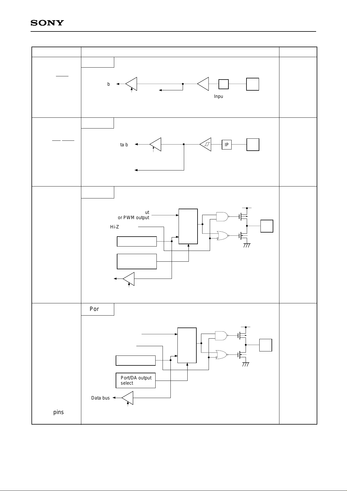
PE0/INT0
PE1/EC/INT2
PE2/PWM0
PE3/PWM1
PE4/DAA0
PE5/DAA1
PE6/DAB0
I/O/
Real time
output
I/O/
Real time
output
I/O
Input/Input
Input/Input/Input
Output/Output
Output/Output
Output/Output
Output/Output
Output/Output
(Port C)
8-bit I/O port, enables to
specify I/O by bit unit.
Data is gated with PPO or
RTO contents by OR-gate
and they are output.
(8 pins)
Real time pulse generator (RTG) output.
Functions as high precision real time
pulse output port. (5 pins)
(Port D)
8-bit I/O port. Enable to specify I/O by 4-bit unit.
Enables to drive 12mA sink current.
(8 pins)
Input pin to request external interruption.
Active when falling edge.
(Port E)
8-bit port.
Lower 2 bits
are input pins
and upper 6
bits are output
External event input
pin for timer/counter.
PWM output pins.
(2 pins)
Input pin to request
external interruption.
Active when falling edge.
pins.
(8 pins)
DA gate pulse output pins.
(4 pins)
PE7/DAB1
AN0 to AN3
PF0/AN4
to
PF3/AN7
PF4/AN8
to
PF7/AN11
SCK0
SO0
SI0
CS0
Output/Output
Input
Input/Input
Output/Input
I/O
Ouput
Input
Input
Analog input pins to A/D converter. (12 pins)
(Port F)
Lower 4 bits are input port and upper 4 bits are output port.
Lower 4 bits also serve as standby release input pin.
(8 pins)
Serial clock (CH0) I/O pin.
Serial data (CH0) output pin.
Serial data (CH0) input pin.
Serial chip select (CH0) input pin.
– 5 –
Symbol I/O Description
PG0 to PG4
PG5/PCK
PG6/EXI0
Input
(Port G)
8-bit input port.
(8 pins)
7 bit general purpose prescaler input pin.
External input pin to FRC capture unit.
PG7/EXI1
(Port H)
PH0 to PH7
Output
8-bit output port ; Medium withstand voltage (12V) and high current
(12mA), N-ch open drain output.
(8 pins)
CXP81952/81960
PI1/RMC
PI2/PWM
PI3/TO/ADJ
PI4/INT1/
NMI
PI5/SCK1
PI6/SO1
PI7/SI1
PJ0 to PJ7
EXTAL
XTAL
TEX
TX
RST
MP
AVDD
AVREF
AVss
VDD
Vss
I/O/Input
I/O/Output
I/O/Output/Output
I/O/Input/Input
I/O/I/O
I/O/Output
I/O/Input
I/O
Input
Output
Input
Output
Input
Input
Input
Remote control receiving circuit input pin.
14-bit PWM output pin.
(Port I)
7-bit I/O port.
I/O port can be
specified by bit
unit.
(7 pins)
Timer/counter, 32kHz oscillation adjustment output
pin.
Input pin to request external interruption and
non-maskable interruption. Active when falling edge.
Serial clock (CH1) I/O pin.
Serial data (CH1) output pin.
Serial data (CH1) input pin.
(Port J)
8-bit I/O port. Function as standby release input can be specified by bit
unit. I/O can be specified by bit unit.
Connecting pin of crystal oscillator for system clock. When supplying
the external clock, input the external clock to EXTAL pin and input
opposite phase clock to XTAL pin.
Connecting pin of crystal oscillator for 32kHz timer clock. When used
as event counter, input to TEX pin and leave TX pin open. (Feedback
resistor is not removed.)
System reset pin of active "L" level.
Microprocessor mode input pin. Always connect to GND.
Positive power supply pin of A/D converter.
Reference voltage input pin of A/D converter.
GND pin of A/D converter.
Positive power supply pin.
GND pin. Connect both Vss pins to GND.
– 6 –
Input/Output Circuit Formats for Pins
CXP81952/81960
Pin
PA0/PPO0
to
PA7/PPO7
PB0/PPO8
to
PB7/PPO15
16 pins
PC0/PPO16
to
PC2/PPO18
PC3/RTO3
to
PC7/RTO7
Port A
Port B
Data bus
Port C
PPO data
Port A or Port B
RD
PPO, RTO data
Port C data
Port C direction
Circuit format
Output becomes active from high
impedance by data writing to port register.
(Every bit)
IP
Input
protection
circuit
When reset
Hi-Z
Hi-Z
8 pins
PD0 to PD7
8 pins
Data bus
Port D
Data bus
RD (Port C)
Port D data
Port D direction
RD (Port D)
(Every 4 bits)
PD0 to 3
PD4 to 7
IP
High
current
12mA
Hi-Z
– 7 –
CXP81952/81960
A
Pin
PE0/INT0
1 pin
PE1/EC/INT2
1 pin
PE2/PWM0
PE3/PWM1
PE4/DAA0
PE5/DAA1
Port E
Data bus
Port E
Data bus
Interruption circuit/
event counter
Port E
DA gate output
or PWM output
Hi-Z control
RD
Port E data
Circuit format
Interruption circuit
RD (Port E)
MPX
IP
Input protection circuit
IP
Input protection circuit
When reset
Hi-Z
Hi-Z
Hi-Z
4 pins
PE6/DAB0
PE7/DAB1
2 pins
Data bus
Port E
Data bus
Port/DA output
select
RD (Port E)
DA gate output
Hi-Z control
Port E data
Port/DA output
select
RD (Port E)
MPX
A
H level
– 8 –
CXP81952/81960
AAA
Pin
AN0 to AN3
4 pins
PF0/AN4
to
PF3/AN7
4 pins
PF4/AN8
to
PF7/AN11
4 pins
Port F
Port F
Data bus
Port F data
RD
(Port F)
Circuit format
Input multiplexer
IP
Input multiplexer
IP
Port/AD select
RD (Port F)
A/D converter
A/D converter
Data bus
IP
Input multiplexer
A/D
converter
When reset
Hi-Z
Hi-Z
Hi-Z
PG0 to PG4
PG5/PCK
6 pins
PG6/EXI0
PG7/EXI1
2 pins
PH0 to PH7
8 pins
Port G
Port G
Port H
Data bus
Port H data
RD (Port H)
Schmitt input
IP
Schmitt input
IP
RD (Port G)
RD (Port G)
Data bus
PG5: To general
purpose prescaler
FRC capture unit
Data bus
Medium withstand
voltage 12V
Large current
12mA
Hi-Z
Hi-Z
Hi-Z
– 9 –
 Loading...