

Sony CXP7500P11, CXP7500P10 Datasheet
Description
The CXP7500P10/7500P11 is a CMOS 8-bit single
chip microcomputer integrating on a single chip an A/D
converter, serial interface, timer/counter, time-base
timer, on-screen display function, I
2
C bus interface,
PWM output, remote control reception circuit, HSYNC
counter, watchdog timer, 32kHz timer/counter besides
the basic configurations of 8-bit CPU, ROM, RAM, I/O
ports.
The CXP7500P10/7500P11 also provides a sleep
function that enables to lower the power consumption.
CXP7500P10/7500P11 is the PROM-incorporated
version of the CXP750096/750010/750097/750011 with
built-in mask ROM. This provides the additional feature
of being able to write directly into the program. Thus, it
is most suitable for evaluation use during system
development and for small-quantity production.
Features
• A wide instruction set (213 instructions) which covers
various types of data
– 16-bit operation/multiplication and division/
Boolean bit operation instructions
• Minimum instruction cycle 167ns at 24MHz operation
122µs at 32kHz operation
• Incorporated ROM 120K bytes
• Incorporated RAM 2496 bytes (Excludes VRAM for on-screen display)
• Peripheral functions
– A/D converter 8-bit 6-channel successive approximation method
(Conversion time of 3.25µs at 16MHz)
– Serial interface 8-bit clock sync type (MSB/LSB first selectable), 1 channel
– Timer 8-bit timer
8-bit timer/counter
19-bit time-base timer
32kHz timer/counter
– On-screen display (OSD) function 24
× 32 dots, 512 character types,
15 character colors, 2 lines × 32 characters,
frame background 8 colors/half blanking,
background on full screen 15 colors/half blanking
edging/shadowing/rounding for every line,
background with shadow for every character, double scanning,
Sprite OSD 24 × 32 dots, 1 screen, 8 colors for every dot
– I
2
C bus interface
– PWM output 8 bits, 8 channels
14 bits, 1 channel
– Remote control reception circuit 8-bit pulse measurement counter, 6-stage FIFO
– HSYNC counter 2 channels
– Watchdog timer
• Interruption 13 factors, 13 vectors, multi-interruption possible
• Standby mode Sleep
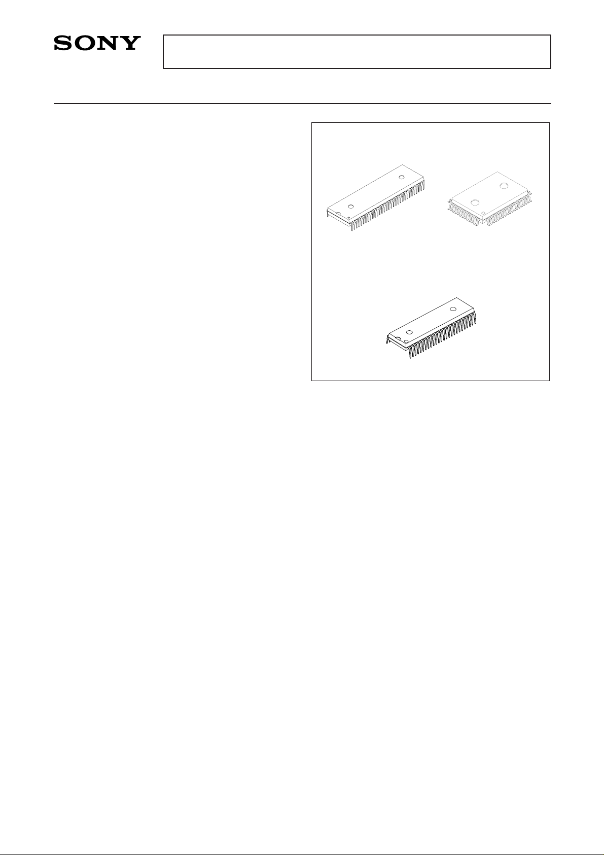
• Package 64-pin plastic SDIP/QFP, 52-pin plastic SDIP
• Piggy/evaluation chip CXP750000 64-pin ceramic PQFP/PSDIP (Supports custom font)
Perchase of Sony's I2C components conveys a licence under the Philips I2C Patent Rights to use these components
in an I2C system, provided that the system conforms to the I2C Standard Specifications as defined by Philips.
CXP7500P10/7500P11
CMOS 8-bit Single Chip Microcomputer
– 1 –
E99104-PS
Sony reserves the right to change products and specifications without prior notice. This information does not convey any license by
any implication or otherwise under any patents or other right. Application circuits shown, if any, are typical examples illustrating the
operation of the devices. Sony cannot assume responsibility for any problems arising out of the use of these circuits.
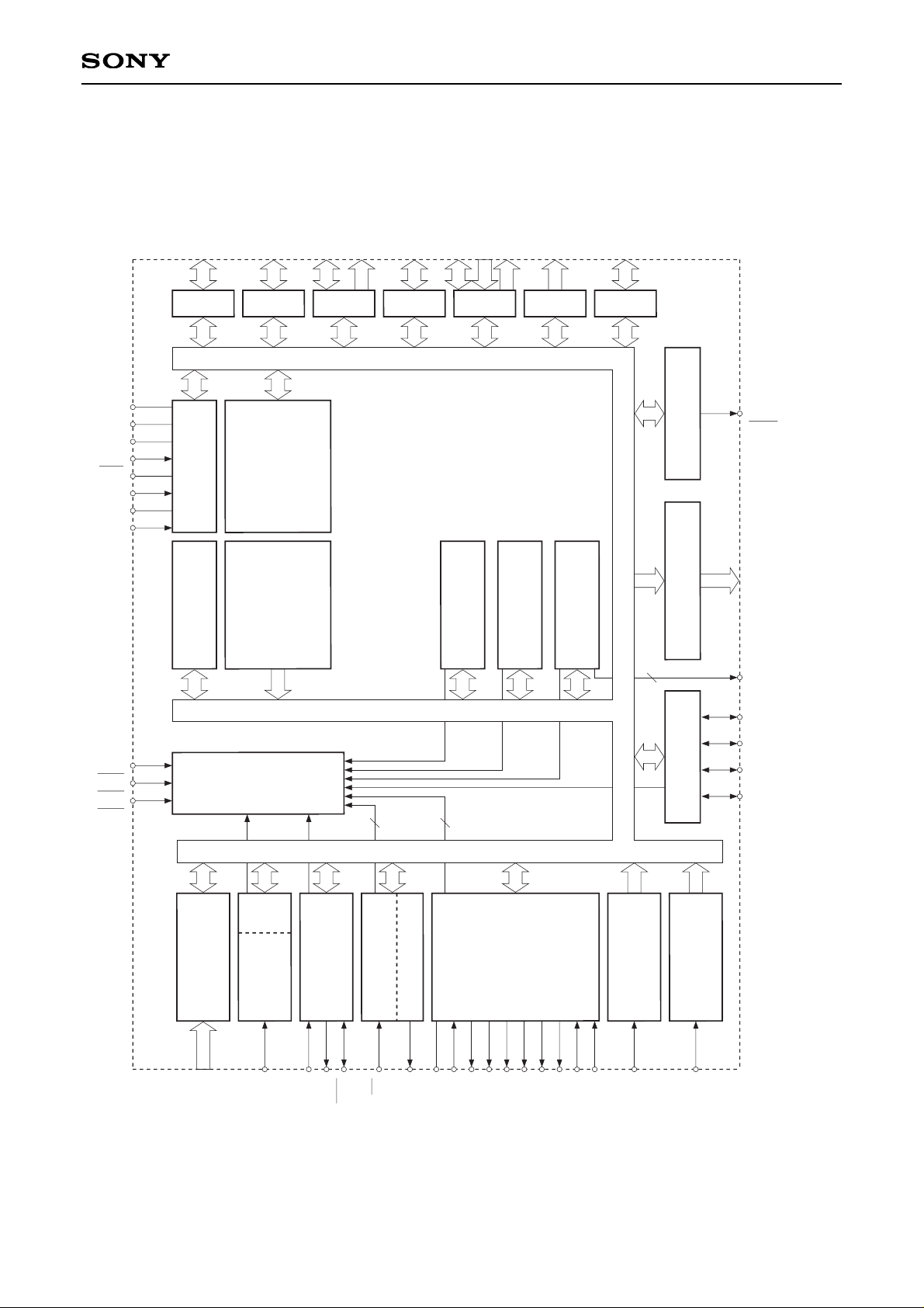
Structure
Silicon gate CMOS IC
64 pin SDIP (Plastic) 64 pin QFP (Plastic)
52 pin SDIP (Plastic)
– 2 –
CXP7500P10/7500P11
A/D CONVERTER
FIFOREMOCON
SERIAL INTERFACE
UNIT
8-BIT TIMER 1
8-BIT TIMER/
COUNTER 0
ON SCREEN
DISPLAY
HSYNC COUNTER 0
HSYNC COUNTER 1
I
2
C BUS
INTERFACE UNIT
8 BITS PWM 8CH (6CH) 14 BITS PWM 1CH
PRESCALER/
TIME-BASE TIMER
WATCHDOG TIMER
32kHz
TIMER/COUNTER
ROM
120K BYTES
RAM
2496 BYTES
CLOCK GENERATOR/
SYSTEM CONTROL
INTERRUPT CONTROLLER
PORT APORT BPORT CPORT DPORT EPORT FPORT G
PG3 to PG6
∗
, PG7
PWM
5
PF0 to PF7
8
PE4 to PE6
3
PE2, PE3
2
PE0, PE1
2
PD0 to PD7
8
PC6, PC7
∗
2
PC0 to PC5
∗
6
PB0 to PB7
8
PA0 to PA7
8
PWM0 to PWM7
ADJ
SCL1
SCL0
SDA1
SDA0
HS1
HS0
VSYNC
HSYNC
YM
YS
I
B
G
R
EXLC
XLC
TO
EC
SCK
SO
SI
RMC
AN0 to AN5
6
2
2
2
INT0
INT1
INT2
TEX
TX
EXTAL
XTAL
V
DD
V
SS
RST
8 (6)
SPC 700αII
CPU CORE
Vpp
Block Diagram
∗
Not incorrporated for 52-pin package.
Parentheses indicate configurations for
52-pin package.
– 3 –
CXP7500P10/7500P11
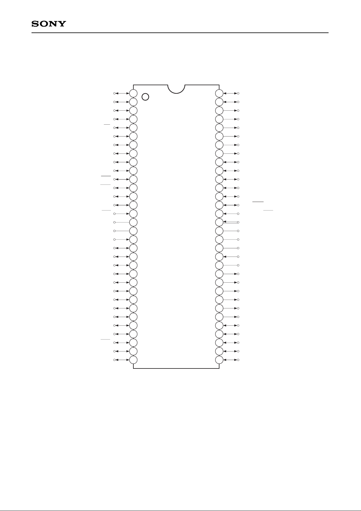
40
39
38
37
36
35
34
33
41
42
43
44
45
46
47
48
49
50
51
52
53
54
55
56
57
58
59
60
63
64
61
62
31
32
2
3
4
5
6
7
8
9
10
11
12
13
14
15
16
17
18
19
20
21
22
23
24
25
26
27
28
29
30
1
V
SS
VDD
Vpp
EXLC
XLC
PE4/YM
PE5/YS
PE6/I
B
G
R
PB0
PB1
PB2
PG3
PG4
PC4
PC5
PC6/PWM6
PC7/PWM7
PF0/PWM0
PF1/PWM1
PF2/PWM2
PF3/PWM3
PF4/SCL0
PF5/SCL1/PWM4
PF6/SDA0
PF7/SDA1/PWM5
PE0/TO/ADJ
PE1/PWM
PE2/TEX/INT0
PE3/TX
PD4/HS0
PC3
PC2
PC1
PC0
PD7/EC
PD6/RMC
PD5/HS1
PD3/SI
PD2/SO
PD1/SCK
PD0/INT2
PA7/HSYNC
PA6/VSYNC
RST
V
SS
PA0/AN0
XTAL
EXTAL
PA5/AN5
PA4/AN4
PA3/AN3
PA2/AN2
PA1/AN1
PB7
PB6
PB5
PB4
PB3
PG7/INT1
PG6
PG5
Pin Assignment (Top View) 64-pin SDIP
Note)
1. Vpp (Pin 46) is left open.
2. Vss (Pins 16 and 48) are both connected to GND.
– 4 –
CXP7500P10/7500P11
VSS
VDD
Vpp
EXLC
XLC
PE4/YM
PE5/YS
PE6/I
B
G
PE1/PWM
PE2/TEX/INT0
PE3/TX
PF3/PWM3
PF4/SCL0
PF5/SCL1/PWM4
PF6/SDA0
PF7/SDA1/PWM5
PE0/TO/ADJ
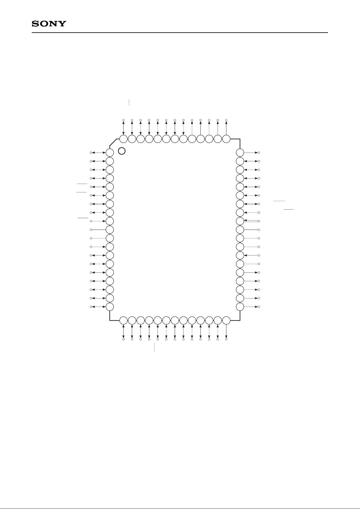
40
39
38
37
36
35
34
33
41
42
43
44
45
46
47
48
49
50
51
PF2/PWM2
PF1/PWM1
PF0/PWM0
PC7/PWM7
PC6/PWM6
PC5
PC4
PC3
PC2
PC1
PC0
PD7/EC
PD6/RMC
52
53
54
55
56
57
58
59
60
63
64
61
62
R
PB0
PB1
PB2
PG3
PG4
PG5
PG6
PG7/INT1
PB3
PB4
PB5
PB6
31
32
20
21
22
23
24
25
26
27 28
29
30
PD4/HS0
PD5/HS1
PD3/SI
PD2/SO
PD1/SCK
PD0/INT2
PA7/HSYNC
PA6/VSYNC
RST
V
SS
PA0/AN0
XTAL
EXTAL
PA5/AN5
PA4/AN4
PA3/AN3
PA2/AN2
PA1/AN1
PB7
2
3
4
5
6
7
8
9
10
11
12
13
14
15
16
17
18
19
1
Pin Assignment (Top View) 64-pin QFP
Note)
1. Vpp (Pin 40) is left open.
2. Vss (Pins 10 and 42) are both connected to GND.

– 5 –
CXP7500P10/7500P11
40
39
38
37
36
35
34
33
41
42
43
44
45
46
47
48
49
50
51
52
31
32
27
28
29
30
2
3
4
5
6
7
8
9
10
11
12
13
14
15
16
17
18
19
20
21
22
23
24
25
26
1
PD4/HS0
PD7/EC
PD6/RMC
PD5/HS1
PD3/SI
PD2/SO
PD1/SCK
PD0/INT2
PA7/HSYNC
PA6/VSYNC
RST
V
SS
PA0/AN0
XTAL
EXTAL
PA5/AN5
PA4/AN4
PA3/AN3
PA2/AN2
PA1/AN1
PB7
PB6
PB5
PB4
PB3
PG7/INT1
VSS
VDD
Vpp
EXLC
XLC
PE4/YM
PE5/YS
PE6/I
B
G
R
PB0
PB1
PB2
PF0/PWM0
PF1/PWM1
PF2/PWM2
PF3/PWM3
PF4/SCL0
PF5/SCL1/PWM4
PF6/SDA0
PF7/SDA1/PWM5
PE0/TO/ADJ
PE1/PWM
PE2/TEX/INT0
PE3/TX
Pin Assignment (Top View) 52-pin SDIP
Note)
1. Vpp (Pin 38) is left open.
2. Vss (Pins 12 and 40) are both connected to GND.

– 6 –
CXP7500P10/7500P11
(Port A)
8-bit I/O port.
I/O can be set in a
unit of single bits.
(8 pins)
(Port B)
8-bit I/O port. I/O can be set in a unit of single bits.
(8 pins)
(Port C)
Lower 6 bits are I/O ports; I/O can be set in a unit of single bits. Upper
2 bits are output port and large current (12mA) N-channel open drain
output. Upper 2 bits are medium drive voltage (12V); lower 6 bits are
5V drive.
(8 pins)
(Port D)
8-bit I/O port. I/O
can be set in a
unit of single bits.
Can drive 12mA
sink current.
(8 pins)
(Port E)
Bits 0 and 1 are I/O
port; I/O can be set
in a unit of single
bits.
Bits 2 and 3 are
input port. Bits 4, 5
and 6 are output
port.
(7 pins)
Pin Description
Symbol
PA0/AN0
to
PA5/AN5
PA6/VSYNC
PA7/HSYNC
PB0 to PB7
PC0 to PC5
∗
PC6/PWM6∗ to
PC7/PWM7
∗
PD0/INT2
PD1/SCK
PD2/SO
PD3/SI
PD4/HS0
PD5/HS1
PD6/RMC
PD7/EC
PE0/TO/ADJ
PE1/PWM
PE2/TEX/INT0
PE3/TX
PE4/YM
PE5/YS
PE6/I
B
G
R
I/O/
Analog input
I/O/Input
I/O/Input
I/O
I/O
Output/Output
I/O/Input
I/O/I/O
I/O/Output
I/O/Input
I/O/Input
I/O/Input
I/O/Input
I/O/Input
I/O/Output/
Output
I/O/Output
Input/Input/
Input
Input
Output/Output
Output/Output
Output/Output
Output
Output
Output
I/O
Description
Analog inputs to A/D converter.
(6 pins)
OSD display vertical sync signal input.
OSD display horizontal sync signal input.
8-bit PWM output.
(2 pins)
External interruption request input. Active at the
falling edge.
Serial clock I/O.
Serial data output.
Serial data input.
HSYNC counter (CH0) input.
HSYNC counter (CH1) input.
Remote control reception circuit input.
External event input for timer/counter.
Rectangular wave output
for 8-bit timer/counter.
14-bit PWM output.
Connects a crystal for
32kHz timer/counter
clock oscillation. When
used as an event
counter, input to TEX pin and leave TX pin open.
TEX oscillation
frequency dividing output.
External interruption
request input. Active at
the falling edge.
OSD display 6-bit output.
(6 pins)
∗
Not incorporated for 52-pin package.
– 7 –
CXP7500P10/7500P11
(Port F)
8-bit output port
and large current
(12mA) N-channel
open drain output.
Lower 4 bits are
medium drive
voltage (12V); upper
4 bits are 5V drive.
(8 pins)
(Port G)
5-bit I/O port. I/O can be set in a unit of single bits.
(5 pins)
Connects a crystal for system clock oscillation. When a clock is
supplied externally, input to EXTAL pin and input a reversed phase
clock to XTAL pin.
System reset; active at Low level.
OSD display clock oscillation I/O. Oscillation frequency is determined
by the external L and C.
Positive power supply for incorporated PROM writing.
Leave this pin open during normal operation.
Positive power supply.
GND. Connect two Vss pins to GND.
8-bit PWM output.
(4 pins)
I2C bus interface transfer clock I/O.
(2 pins)
I2C bus interface transfer data I/O.
(2 pins)
Symbol
PF0/PWM0 to
PF3/PWM3
PF4/SCL0
PF5/SCL1/
PWM4
PF6/SDA0
PF7/SDA1/
PWM5
PG3 to PG6
∗
PG7/INT1
EXTAL
XTAL
RST
EXLC
XLC
Vpp
VDD
Vss
Output/Output
Output/I/O
Output/I/O/
Output
Output/I/O
Output/I/O/
Output
I/O
I/O/Input
Input
Input
Input
I/O Description
8-bit PWM output.
8-bit PWM output.
External interruption request input.
Active at the falling edge.
∗
Not incorporated for 52-pin package.
– 8 –
CXP7500P10/7500P11
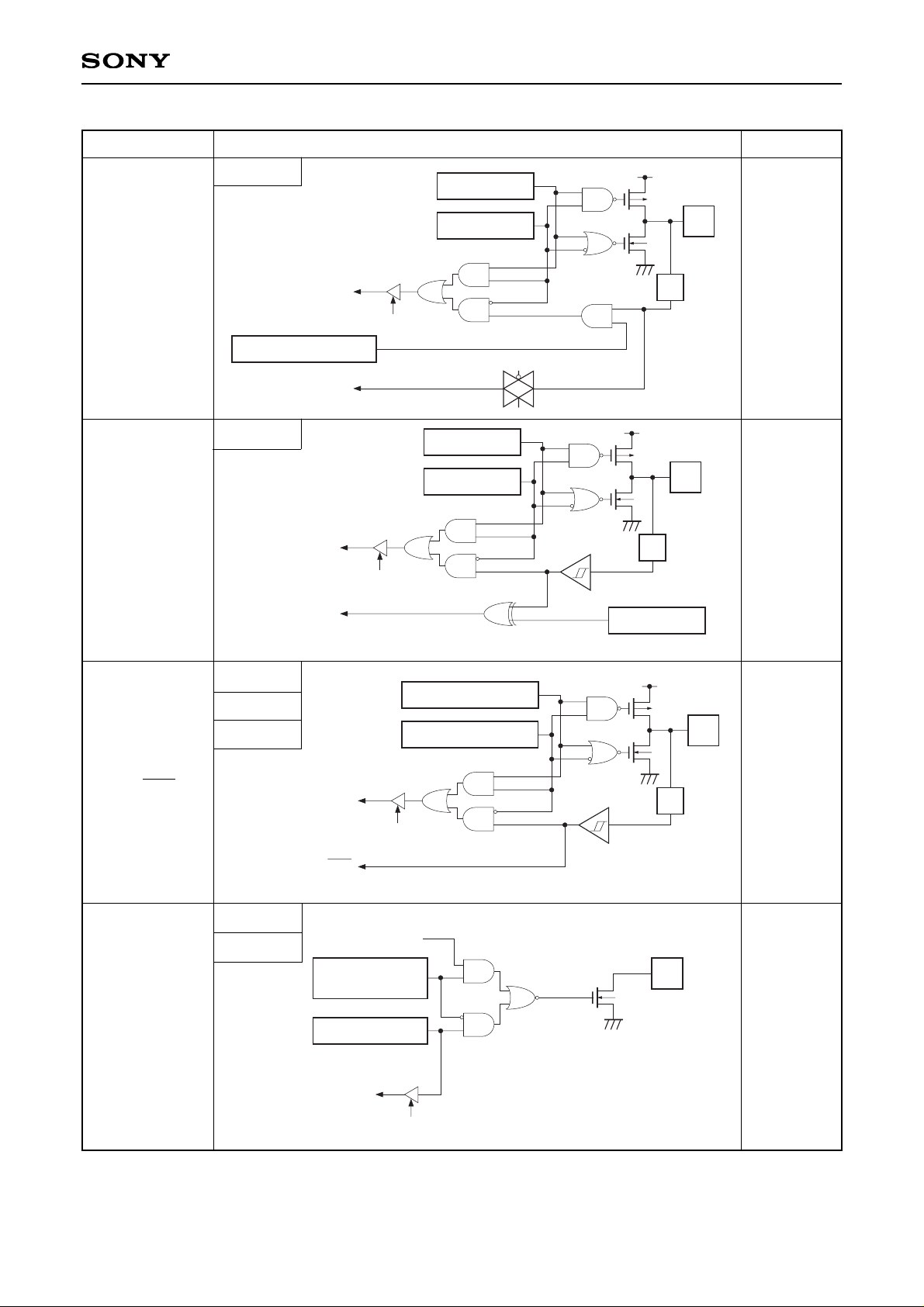
Input/Output Circuit Formats for Pins
Port A
Port A
Port B
Port C
6 pins
2 pins
19 pins
Hi-Z
Hi-Z
Hi-Z
Pin After a resetCircuit format
PA6/VSYNC
PA7/HSYNC
PB0 to PB7
PC0 to PC5
∗
PG3 to PG6
∗
PG7/INT1
PA0/AN0
to
PA5/AN5
Port G
Ports C, F data
Ports C, F function
selection
“0” after a reset
“1” after a reset
PWM0 to PWM3
PWM6, PWM7
∗
12V drive voltage
Large current 12mA
∗
RD (Ports C, F)
Internal data bus
Port C
6 pins
PC6/PWM6
∗
PC7/PWM7
∗
PF0/PWM0
to
PF3/PWM3
Hi-Z
Port F
∗
Not incorporated for 52-pin package.
Internal data bus
Port A function selection
“0” after a reset
A/D converter
RD (Port A)
Input multiplexer
Port A direction
“0” after a reset
Port A data
Port A direction
“0” after a reset
Port A data
IP
Input
protection
circuit
Internal data bus
HSYNC, VSYNC
Internal data bus
RD (Port A)
RD (Ports B, C, G)
INT1
Ports B, C, G data
Ports B, C, G direction
“0” after a reset
Schmitt input
PB0 to PB2
Schmitt input only
for PG7
IP
Input polarity
“0” after a reset
IP
 Loading...