

Sony CXP750000 Datasheet
CMOS 8-bit Single Chip Microcomputer
Description
The CXP750000 is a CMOS 8-bit single chip microcomputer of piggyback/evaluator combined type,
which is developed for evaluating the function of the
CXP750096/750010.
Note that the CXP750000 corresponds to the custom
font.
Features
• A wide instruction set (211 instructions) which covers
various types of data
–16-bit operation/multiplication and division/ Boolean
bit operation instructions
• Minimum instruction cycle 167ns at 24MHz operation
250ns at 16MHz operation
122µs at 32kHz operation
• Applicable EPROM CXP27C702K (Maximum 120K bytes are available.)
• Incorporated RAM 2496 bytes (Excludes VRAM for on-screen display )
• EPROM for custom font 57K bytes
• Peripheral functions
–A/D converter 8 bits, 6 channels, successive approximation method
(Conversion time of 3.25µs at 16MHz)
–Serial interface 8-bit clock sync type, 1 channel
–Timer 8-bit timer
8-bit timer/counter
19-bit time-base timer
32kHz timer/counter
–On-screen display (OSD) 24 × 32 dots, 512 character types, 15 character colors, 32 characters × 2 lines
frame background 8 colors/half blanking
background on full screen 15 colors/half blanking
edging/shadowing/rounding for every line
background with shadow for every character, double scanning
sprite OSD; 24 × 32 dots, 1 screen, 8 colors for every dot
–I2C bus interface
–PWM output 8 bits, 8 channels
14 bits, 1 channel
–Remote control unit receive circuit
8-bit pulse measurement counter, 6-stage FIFO
–HSYNC counter 2 channels
–Watchdog timer
• Interruption 13 factors, 13 vectors, multi-interruption possible
• Standby mode Sleep
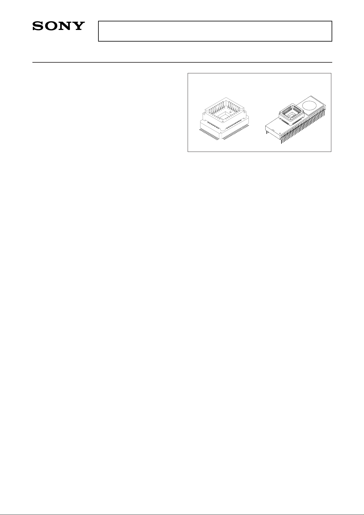
• Package CXP750000 64-pin ceramic PQFP/PSDIP (Supports custom font)
Note) Mask option depends on the type of the CXP750000. Refer to the Product List for details.
Perchase of Sony's I2C components conveys a licence under the Philips I2C Patent Rights to use these components
in an I2C system, provided that the system conforms to the I2C Standard Specifications as defined by Philips.
– 1 –
E98613-PS
Sony reserves the right to change products and specifications without prior notice. This information does not convey any license by
any implication or otherwise under any patents or other right. Application circuits shown, if any, are typical examples illustrating the
operation of the devices. Sony cannot assume responsibility for any problems arising out of the use of these circuits.
CXP750000
64 pin PQFP (Ceramic) 64 pin PSDIP (Ceramic)
Structure
Silicon gate CMOS IC
Piggy/evaluation chip
– 2 –
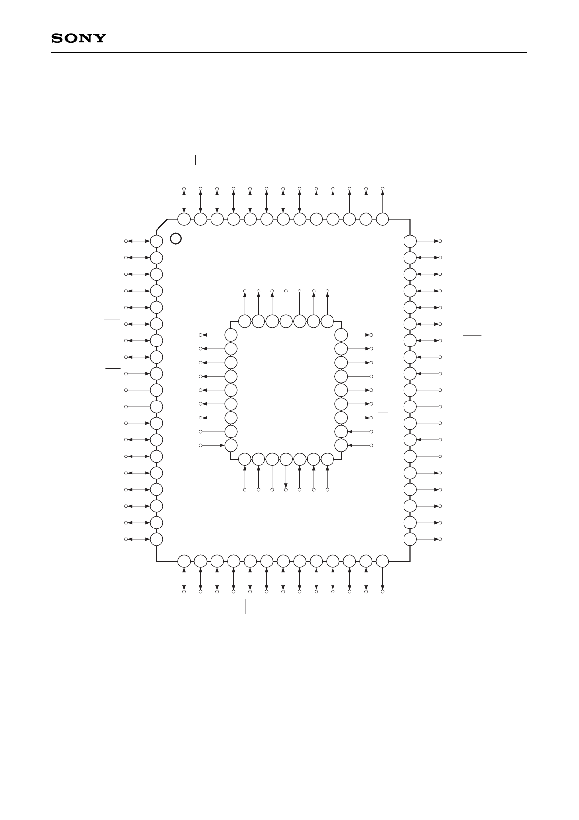
CXP750000
VSS
VDD
NC
EXLC
XLC
PE4/YM
PE5/YS
PE6/I
B
G
PE1/PWM
PE2/TEX/INT0
PE3/TX
PF3/PWM3
PF4/SCL0
PF5/SCL1/PWM4
PF6/SDA0
PF7/SDA1/PWM5
PE0/TO/ADJ
40
39
38
37
36
35
34
33
41
42
43
44
45
46
47
48
49
50
51
PF2/PWM2
PF1/PWM1
PF0/PWM0
PC7/PWM7
PC6/PWM6
PC5
PC4
PC3
PC2
PC1
PC0
PD7/EC
PD6/RMC
52
53
54
55
56
57
58
59
60
63
64
61
62
R
PB0
PB1
PB2
PG3
PG4
PG5
PG6
PG/7INT1
PB3
PB4
PB5
PB6
31
32
20
21
22
23
24
25
26 27
28
29
30
PD4/HS0
PD5/HS1
PD3/SI
PD2/SO
PD1/SCK
PD0/INT2
PA7/HSYNC
PA6/VSYNC
RST
V
SS
PA0/AN0
XTAL
EXTAL
PA5/AN5
PA4/AN4
PA3/AN3
PA2/AN2
PA1/AN1
PB7
2
3
4
5
6
7
8
9
10
11
12
13
14
15
16
17
18
19
1
D7
NC
A8
D6
A9
A11
OE
A10
CE
NC
D0
A6
A13
D5
D4
D3
A16
D2
D1
GND
A14
V
DD
A12
A7
A15
NC
A5
A4
A3
A2
A1
A0
31
32
20
21
22
23
24
25
26
27
28
29
30
2
3
4
5
6
7
8
9
10
11
12
13
14
15
16
17
18
19
1
Note) 1. NC (Pin 40) is left open.
2. Vss (Pins 10 and 42) are both connected to GND.
CXP750000
Pin Assignment in Piggyback Mode (Top View)
– 3 –
CXP750000
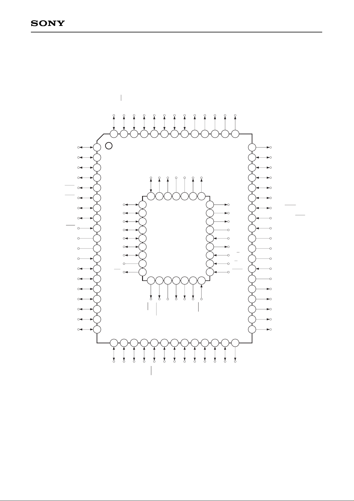
VSS
VDD
NC
EXLC
XLC
PE4/YM
PE5/YS
PE6/I
B
G
PE1/PWM
PE2/TEX/INT0
PE3/TX
PF3/PWM3
PF4/SCL0
PF5/SCL1/PWM4
PF6/SDA0
PF7/SDA1/PWM5
PE0/TO/ADJ
40
39
38
37
36
35
34
33
41
42
43
44
45
46
47
48
49
50
51
PF2/PWM2
PF1/PWM1
PF0/PWM0
PC7/PWM7
PC6/PWM6
PC5
PC4
PC3
PC2
PC1
PC0
PD7/EC
PD6/RMC
52
53
54
55
56
57
58
59
60
63
64
61
62
R
PB0
PB1
PB2
PG3
PG4
PG5
PG6
PG7/INT1
PB3
PB4
PB5
PB6
31
32
20
21
22
23
24
25
26 27
28
29
30
PD4/HS0
PD5/HS1
PD3/SI
PD2/SO
PD1/SCK
PD0/INT2
PA7/HSYNC
PA6/VSYNC
RST
V
SS
PA0/AN0
XTAL
EXTAL
PA5/AN5
PA4/AN4
PA3/AN3
PA2/AN2
PA1/AN1
PB7
2
3
4
5
6
7
8
9
10
11
12
13
14
15
16
17
18
19
1
I/T
NC
A8
MON
A9
A11
HALT
A10
E/P
NC
RD
A6/D6
A13
RST
C1
C2
A16
SYNC
WR
GND
A14
V
DD
A12
A7/D7
A15
NC
A5/D5
A4/D4
A3/D3
A2/D2
A1/D1
A0/D0
31
32
20
21
22
23
24
25
26
27
28
29
30
2
3
4
5
6
7
8
9
10
11
12
13
14
15
16
17
18
19
1
Note) 1. NC (Pin 40) is left open.
2. Vss (Pins 10 and 42) are both connected to GND.
CXP750000
Pin Assignment in Evaluator Mode (Top View)
 Loading...