

Sony CXP7400P10 Datasheet

CMOS 8-bit Single Chip Microcomputer
Description
The CXP7400P10 is a CMOS 8-bit microcomputer
integrating on a single chip an A/D converter, serial
interface, timer/counter, time-base timer, capture
timer/counter, remote control receive circuit, PWM
output, and the like besides the basic configurations
of 8-bit CPU, ROM, RAM, and I/O port.
The CXP7400P10 also provides the sleep/stop
functions that enable lower power consumption.
The CXP7400P10 is the PROM-incorporated
version of the CXP740056/740096/740010 with builtin mask ROM. This provides the additional feature of
being able to write directly into the program. Thus, it
is most suitable for evaluation use during system
development and for small-quantity production.
Features
• A wide instruction set (211 instructions) which covers various types of data.
— 16-bit arithmetic/multiplication and division/Boolean bit operation instructions
• Minimum instruction cycle 167ns at 24MHz operation (4.5 to 5.5V)
333ns at 12MHz operation (2.7 to 5.5V)
122µs at 32kHz operation (2.7 to 5.5V)
• Incorporated PROM capacity 120K bytes
• Incorporated RAM capacity 4096 bytes
• Peripheral functions
— A/D converter 8 bits, 8 channels, successive approximation method
(Conversion time 10.3µs at 24MHz)
— Serial interface Srart-stop synchronization (UART), 1 channel
Incorporated buffer RAM (Auto transfer for 1 to 32 bytes), 2 channels
8-bit clock syncronization (MSB/LSB first selectable), 1 channel
— Timer 8-bit timer 2 channels, 8-bit timer/counter 2 channels,
19-bit time-base timer, 16-bit capture timer/counter
32kHz timer/counter
— Remote control receive circuit Noise elimination circuit
8-bit pulse measuring counter, 6-stage FIFO
— PWM output 12 bits, 2 channels
• Interruption 22 factors, 15 vectors, multi-interruption possible
• Standby mode Sleep/stop
• Package 100-pin plastic QFP/LQFP
– 1 –
E98518-PS
Sony reserves the right to change products and specifications without prior notice. This information does not convey any license by
any implication or otherwise under any patents or other right. Application circuits shown, if any, are typical examples illustrating the
operation of the devices. Sony cannot assume responsibility for any problems arising out of the use of these circuits.
CXP7400P10
100 pin QFP (Plastic) 100 pin LQFP (Plastic)
Structure
Silicon gate CMOS IC
– 2 –
CXP7400P10
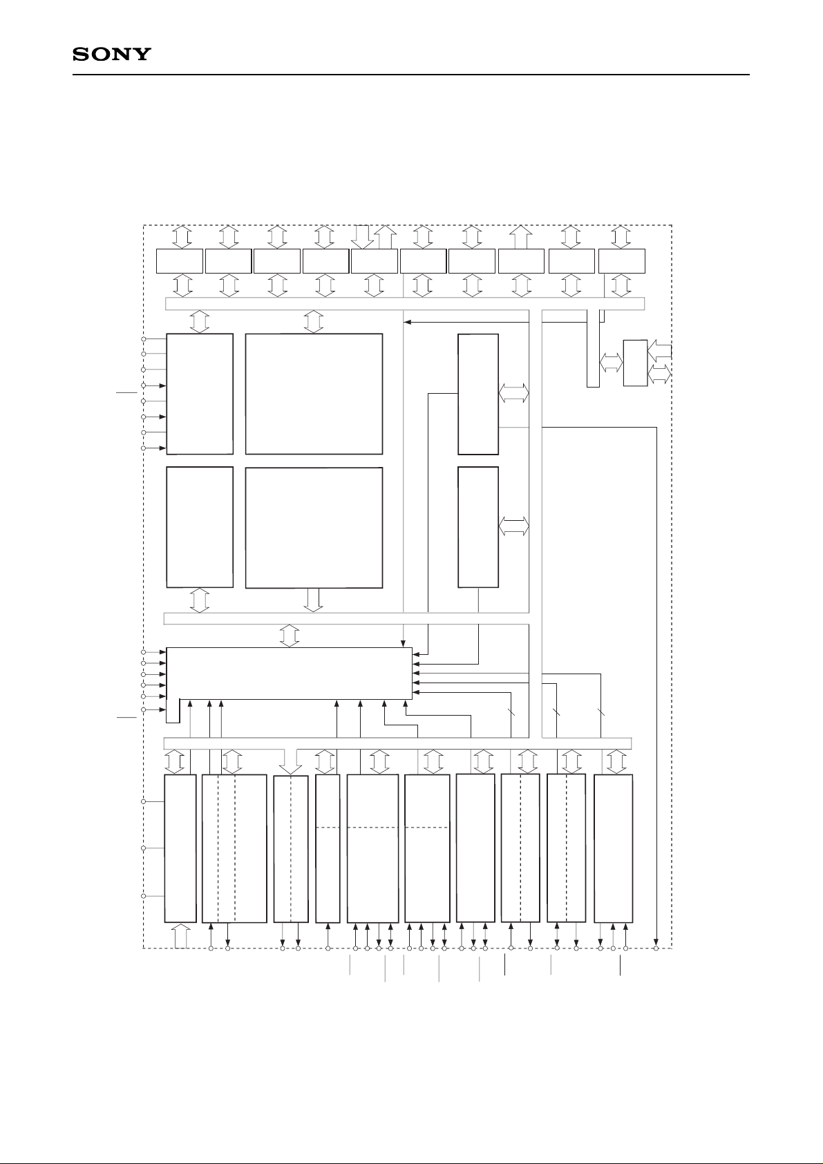
PF0 to PF7
8
RAM
4096
BYTES
INTERRUPT CONTROLLER
A/D CONVERTER
INT3
INT1
INT0
INT2
AN0 to AN11
12
RST
V
DD
V
SS
EXTAL
XTAL
AV
REF
AV
SS
RxD
TxD
PROM
120K
BYTES
2
CLOCK
GENERATOR/
SYSTEM CONTROL
PORT A
2
6
PA0 to PA7
PB0 to PB7
PC0 to PC7
PD0 to PD7
PE0 to PE1
PE2 to PE7
PG0 to PG7
PI1 to PI7
PORT B
PORT C
PORT D
PORT E
PORT F
PORT G
PORT I
PH0 to PH7
PORT H
UART RECEIVER
UART TRANSMITTER
UART BAUD RATE
GENERATOR
8
8
8
8
8
7
INT4
NMI
2
PWM0
12-BIT PWM GENERATOR 0
12-BIT PWM GENERATOR 1
PWM1
REMOCON IN
BUFFER
RAM
CS0
SI0
SO0
SCK0
SERIAL
INTERFACE
UNIT (CH1)
16-BIT CAPTURE
TIMER/COUNTER 4
TO2
8-BIT TIMER/COUNTER 0
8-BIT TIMER 1
EC0
CINT
EC2
SERIAL INTERFACE UNIT
(CH2)
SI2
SO2
SCK2
PJ0 to PJ7
PORT J
8
AV
DD
RMC
CS1
SI1
SO1
SCK1
PRESCALER/
TIME-BASE TIMER
BUFFER
RAM
TX
TEX
32kHz
TIMER/COUNTER
2
5
PORT K
PK3 to PK7
PK1 to PK2
FIFO
SERIAL
INTERFACE
UNIT (CH0)
TO0
8-BIT TIMER/COUNTER 2
8-BIT TIMER 3
EC1
TO1
2
ADJ
Vpp
SPC 700 αII
CPU CORE
8
Block Diagram

– 3 –
CXP7400P10
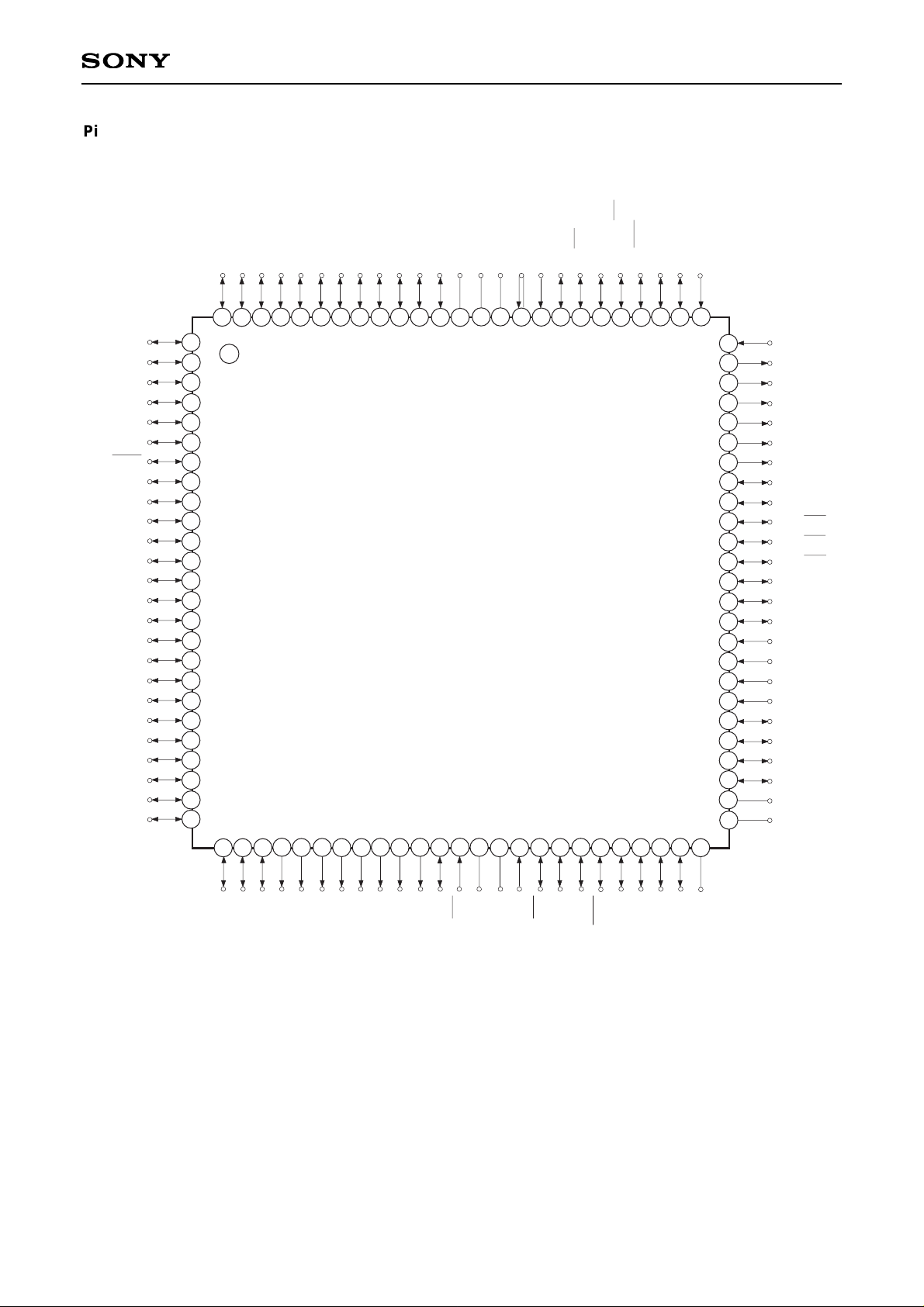
Pin Assignment (Top View) 100-pin QFP package
2
3
4
5
6
7
8
9
10
11
12
13
14
15
16
17
18
19
20
21
22
23
24
25
26
27
28
29
30
40
39
38
37
36
35
34
31
32
33
41
42
43
44
45
46
47
48
49
50
51
52
53
54
55
56
57
58
59
60
70
69
68
67
63
64
65
66
61
62
71
72
73
74
81
82
83
84
75
76
77
78
88
87
86
85
79
89
90
100
99
98
97
96
95
94
91
92
93
1
80
PI6/SO1
PI7/SI1
PE0/INT0
PE1/INT2
PE2/PWM0
PE3/PWM1
PE4
PE5
PE6
PE7
PG0/TxD
PG1/RxD
PG2/EC0
PG3/EC1
PG4/EC2
PG5/INT3
PG6/INT4
PG7/CINT
AN0
AN1
AN2
AN3
PF0/AN4
PF1/AN5
PF2/AN6
PF3/AN7
AV
DD
AVREF
AVSS
PF4/AN8
PC5
PC4
PC3
PC2
PC1
PC0
PB7/SI2
PB6/SO2
PB5/SCK2
PB4/TO2
PB3
PB2
PB1
PB0
PJ7
PJ6
PJ5
PJ4
PJ3
PJ2
PJ1
PJ0
PD7
PD6
PD5
PD4
PD3
PD2
PD1
PD0
PC6
PC7
PA0
PA1
PA2
PA3
PA4
PA5
PA6
PA7
Vpp
V
DD
V
SS
PK1/TX
PK2/TEX
PI1/RMC
PI2/NMI
PI3/TO0/ADJ
PI4/INT1/CS1
PI5/SCK1
PH7
PH6
PH5
PH4
PH3
PH2
PH1
PH0
PK7/TO1
RST
V
SS
XTAL
EXTAL
PK6/CS0
PK5/SI0
PK4/SO0
PK3/SCK0
PF7/AN11
PF6/AN10
PF5/AN9
Note) 1. Vpp (Pin 90) is left open.
2. VSS (Pins 41 and 88) are both connected to GND.
– 4 –
CXP7400P10
2
3
4
5
6
7
8
9
10
11
12
13
14
15
16
17
18
19
20
21
22
23
24
25
40
39
38
37
36
35
34
31
32
33
41
42
43
44
45
46
47
48
49
50
51
52
53
54
55
56
57
58
59
60
70
69
68
67
63
64
65
66
61
62
71
72
73
74
81
82
83
84
75
76
77
78
88
87
86
85
79
89
90
100
99
98
97
96
95
94
91
92
93
1
80
PI6/SO1
PI7/SI1
PE0/INT0
PE1/INT2
PE2/PWM0
PE3/PWM1
PE4
PE5
PE6
PE7
PG0/TxD
PG1/RxD
PG2/EC0
PG3/EC1
PG4/EC2
PG5/INT3
PG6/INT4
PG7/CINT
AN0
AN1
AN2
AN3
PF0/AN4
PF1/AN5
PF2/AN6
PC3
PC2
PC1
PC0
PB7/SI2
PB6/SO2
PB5/SCK2
PB4/TO2
PB3
PB2
PB1
PB0
PJ7
PJ6
PJ5
PJ4
PJ3
PJ2
PJ1
PJ0
PD7
PD6
PD5
PC6
PC7
PA0
PA1
PA2
PA3
PA4
PA5
PA6
PA7
Vpp
V
DD
V
SS
PK1/TX
PK2/TEX
PI1/RMC
PI2/NMI
PI3/TO0/ADJ
PI4/INT1/CS1
PI5/SCK1
PH2
PH1
PH0
PK7/TO1
RST
V
SS
XTAL
EXTAL
PK6/CS0
PK5/SI0
PK4/SO0
PK3/SCK0
PF7/AN11
PF6/AN10
PF5/AN9
PH7
PH6
PH5
PH4
PH3
26
27
28
29
30
PD4
PD3
PD2
PD1
PD0
PF4/AN8
AV
SS
PF3/AN7
AV
DD
AVREF
PC4
PC5
Pin Assignment (Top View) 100-pin LQFP package
Note) 1. Vpp (Pin 88) is left open.
2. VSS (Pins 39 and 86) are both connected to GND.

– 5 –
CXP7400P10
(Port A)
8-bit I/O port. I/O can be set in a unit of single bits.
Incorporation of pull-up resistor can be set through the program in a unit of
single bits.
(8 pins)
(Port C)
8-bit I/O port. I/O can be set in a unit of single bits. Incorporation of pull-up
resistor can be set through the program in a unit of single bits.
(8 pins)
(Port D)
8-bit I/O port. I/O can be set in a unit of single bits. Can drive 12mA sink
current. Incorporation of pull-up resistor can be set through the program in a
unit of single bits.
(8 pins)
(Port E)
8-bit port. Lower 2 bits are
for input; upper 6 bits are for
output.
(8 pins)
(Port F)
8-bit I/O port. I/O can be set
in a unit of single bits.
PF4 to PF7 can be set in a
unit of single bits as standby
release inputs.
Incorporation of pull-up
resistor can be set through
the program in a unit of
single bits.
(8 pins)
Analog inputs to A/D converter.
(8 pins)
Pin Description
Symbol
PA0 to PA7
PC0 to PC7
PD0 to PD7
PE0/INT0
PE1/INT2
PE2/PWM0
PE3/PWM1
PE4 to PE7
PF0/AN4
to
PF7/AN11
I/O
I/O
I/O
Input/Input
Input/Input
Output/Output
Output/Output
Output
I/O/Input
I/O
Description
(Port B)
8-bit I/O port. I/O can be set
in a unit of single bits.
Incorporation of pull-up
resistor can be set through
the program in a unit of
single bits.
(8 pins)
External interrupt inputs.
(2 pins)
12-bit PWM outputs.
(2 pins)
16-bit timer/counter rectangular wave output.
Serial clock I/O (CH2).
Serial data output (CH2).
Serial data input (CH2).
I/O
I/O/Output
I/O/I/O
I/O/Output
I/O/Input
PB0 to PB3
PB4/TO2
PB5/SCK2
PB6/SO2
PB7/SI2

– 6 –
CXP7400P10
(Port H)
8-bit output port. Operated as N-ch open drain output for medium voltage
drive (12V) and large current (12mA).
(8 pins)
(Port I)
7-bit I/O port. I/O can be set
in a unit of single bits.
Incorporation of pull-up
resistor can be set through
the program in a unit of
single bits.
(7 pins)
(Port J)
8-bit I/O port. I/O can be set in a unit of single bits.
Standby release input can be set in a unit of single bits.
Incorporation of pull-up resistor can be set through the program in a unit of
single bits.
(8 pins)
(Port K)
7-bit port. Lower 2 bits are for
input; upper 5 bits are for I/O.
I/O can be set in a unit of
single bits.
For PK3 to PK7, incorporation
of pull-up resistor can be set
through the program in a unit
of single bits.
(7 pins)
UART transmission data output.
UART reception data input.
External event input for 8-bit timer/counter 0.
External event input for 8-bit timer/counter 2.
External event input for 16-bit timer/counter.
External capture input to 16-bit timer/counter.
Remote control receiver circuit input.
Non-maskable interrupt input.
Output for the 8-bit timer/counter 1
rectanguler waves and TEX oscillation
frequency demultiplication.
Serial clock I/O (CH1).
Serial data output (CH1).
Serial data input (CH1).
Crystal connectors for 32-kHz timer/counter
clock oscillation circuit.
For usage as event counter, connect clock
oscillation source to TEX, and leave TX
open.
Serial clock I/O (CH0).
Serial data output (CH0).
Serial data input (CH0).
Chip select input for serial inteface (CH0).
8-bit timer/counter 3 rectangular wave output.
Symbol
PG0/TxD
PG1/RxD
PG2/EC0
PG3/EC1
PG4/EC2
PG5/INT3
PG6/INT4
PG7/CINT
PH0 to PH7
PI1/RMC
PI2/NMI
PI3/TO0/
ADJ
PI4/INT1/
CS1
PI5/SCK1
PI6/SO1
PI7/SI1
PJ0 to PJ7
PK3/SCK0
PK4/SO0
PK5/SI0
PK6/CS0
PK7/TO1
I/O/Output
I/O/Input
I/O/Input
I/O/Input
I/O/Input
I/O/Input
I/O/Input
I/O/Input
Output
I/O/Input
I/O/Input
I/O/Output/
Output
I/O/Input/
Input
I/O/I/O
I/O/Output
I/O/Input
I/O
I/O/I/O
I/O/Output
I/O/Input
I/O/Input
I/O/Output
I/O
Description
Chip select input for serial
interface (CH1).
External
interrupt input.
(Port G)
8-bit I/O port. I/O can be set
in a unit of single bits.
Incorporation of pull-up
resistor can be set through
the program in a unit of
single bits.
(8 pins)
PK1/TX
PK2/TEX
Input
Input/Input
External interrupt inputs.
(2 pins)

– 7 –
CXP7400P10
Analog inputs to A/D converter.
(4 pins)
Connects a crystal for system clock oscillation. When a clock is supplied
externally, input it to EXTAL pin and input a reversed phase clock to XTAL
pin.
System reset; active at Low level.
Positive power supply pin for incorporated PROM writing.
Leave this pin open for normal operation.
(Connected to VDD internally.)
Positive power supply of A/D converter.
Reference voltage input of A/D converter.
GND of A/D converter.
Positive power supply.
GND. Connect both VSS pins to GND.
Symbol
I/O
Description
EXTAL
XTAL
Input
AN0 to AN3
RST
Vpp
AVDD
AVREF
AVSS
VDD
VSS
Input
Input
Input

– 8 –
CXP7400P10
18 pins
Hi-Z
Hi-Z
After a reset
PA0 to PA7
PB0
PB2
PC0 to PC7
PB4/TO2
PI3/TO0/ADJ
PK7/TO1
3 pins
Internal data bus
RD (Ports A, B, C)
IP
A
Ports A, B, C data
“0” after a reset
∗
Ports A, B, C direction
Pull-up resistor
“0” after a reset
∗
Pull-up transistors
approx. 100kΩ (VDD = 4.5 to 5.5V)
approx. 150kΩ (VDD = 2.7 to 3.3V)
I/O Circuit Format for Pins
Pin
Circuit format
2 pins
Hi-Z
PB1
PB3
Internal data bus
RD (Port B)
IP
A
Port B data
“0” after a reset
∗
Port B direction
Pull-up resistor
“0” after a reset
∗
Pull-up transistors
approx. 100kΩ (VDD = 4.5 to 5.5V)
approx. 150kΩ (VDD = 2.7 to 3.3V)
Schmitt input
Internal
data bus
RD (Ports B, I, K)
IP
A
Ports B, I, K function
select
“0” after a reset
∗
“0” after a reset
Pull-up resistor
TO2, TO0/ADJ, TO1
“0” after a reset
∗
Pull-up transistors
approx. 100kΩ (V
DD = 4.5 to 5.5V)
approx. 150kΩ (VDD = 2.7 to 3.3V)
Ports B, I, K data
Ports B, I, K direction
Port A
Port B
Port C
Port B
PortB
Port K
Port I
AAA
– 9 –
CXP7400P10
3 pins
Hi-Z
Hi-Z
After a reset
PB5/SCK2
PI5/SCK1
PK3/SCK0
PB6/SO2
PG0/TxD
PI6/SO1
PK4/SO0
4 pins
Internal
data bus
RD (Ports B, I, K)
IP
Ports B, I, K direction
“0” after a reset
∗
∗
Pull-up transistors
approx. 100kΩ (VDD = 4.5 to 5.5V)
approx. 150kΩ (VDD = 2.7 to 3.3V)
Ports B, I, K data
“0” after a reset
Ports B, I, K function
select
SCK2, SCK1, SCK0
Output enable
Output buffer
capability
“0” after a reset
Pull-up resistor
“0” after a reset
Schmitt input
SCK2, SCK1, SCK0
Pin
Circuit format
A
Internal
data bus
RD (Ports B, G, I, K)
IP
Ports B, G, I, K
direction
“0” after a reset
∗
∗
Pull-up transistors
approx. 100kΩ (VDD = 4.5 to 5.5V)
approx. 150kΩ (VDD = 2.7 to 3.3V)
Ports B, G, I, K data
“0” after a reset
Ports B, G, I, K
function select
SO2, TxD, SO1, SO0
Output enable
Output buffer
capability
“0” after a reset
Pull-up resistor
“0” after a reset
Port B
Port I
Port K
Port B
Port G
Port I
Port K
AA

– 10 –
CXP7400P10
14 pins
Hi-Z
Hi-Z
After a reset
PB7/SI2
PG1/RxD
PG2/EC0
PG3/EC1
PG4/EC2
PG5/INT3
PG6/INT4
PG7/CINT
PI1/RMC
PI2/NMI
PI4/INT1/CS1
PI7/SI1
PK5/SI0
PK6/CS0
PE0/INT0
PE1/INT2
2 pins
Internal data bus
RD (Ports B, G, I, K)
Ports B, G, I, K direction
IP
Ports B, G, I, K data
Pull-up resistor
“0” after a reset
“0” after a reset
∗
Schmitt input
SI2, RxD, EC0, EC1, EC2, INT3, INT4, CINT,
RMC, NMI, INT1/CS1, SI1, SI0, CS0
∗
Pull-up transistors
approx. 100kΩ (VDD = 4.5 to 5.5V)
approx. 150kΩ (VDD = 2.7 to 3.3V)
Pin
Circuit format
8 pins
Hi-Z
PD0 to PD7
Internal data bus
RD (Port D)
Port D direction
Port D data
Pull-up resistor
“0” after a reset
∗
2
∗
1
∗
1
Large current
12mA (VDD = 4.5 to 5.5V)
4.5mA (VDD = 2.7 to 3.3V)
∗
2
Pull-up transistors
approx. 100kΩ (VDD = 4.5 to 5.5V)
approx. 150kΩ (VDD = 2.7 to 3.3V)
IP
IP
Schmitt input
RD (Port E)
Internal data bus
INT0, INT2
Port B
Port G
Port I
Port K
Port D
Port E
 Loading...