

Sony CXP5080 Datasheet
CXP5080
CMOS 4-bit Single Chip Microcomputer
Description
CXP5080 is a CMOS 4-bit single chip microcomputer
of piggyback/evaluator combined type which has
been developed for functional evaluation of the
CXP5084/5086.
Features
• Instruction cycle 3.8µs/4.19MHz (CXP5080)
1.9µs/4.19MHz (CXP5080H)
• ROM capacity Maximum 8K bytes (EPROM 27C64, LCC/DIP type 27C64)
• RAM capacity 400 × 4 bits (Including stack, display area)
• 32 general purpose I/O ports
• 16 large current output ports
• LCD controller/driver (Enables to direct drive)
— Enables to specify the segment output of 24, 20 and 16 optionally
— Enables to select program of the duty, 1/2, 1/3 and 1/4
— 1/3 bias
• 2 external interruption input pins
• 8-bit timer, 8-bit timer/event counter and 18-bit time base timer, independently controlled
• Arithmetic and logical operations possible between the entire RAM area, l/O area and the accumulator by
means of memory mapped I/O
• Reference to the entire ROM area is possible with the table look-up instruction
• 2 kinds of power down modes of sleep and stop
• Power on reset circuit (mask option)
• The oscillation circuit may be optionally specified as the crystal oscillation type or the CR oscillation type
• 64-pin ceramic SDIP/QFP
Note) Mask options are determined according to the CXP5080 category.
For details refer to the product list.
Structure
Silicon gate CMOS IC
– 1 –
E61113A7Z-PS
Sony reserves the right to change products and specifications without prior notice. This information does not convey any license by
any implication or otherwise under any patents or other right. Application circuits shown, if any, are typical examples illustrating the
operation of the devices. Sony cannot assume responsibility for any problems arising out of the use of these circuits.
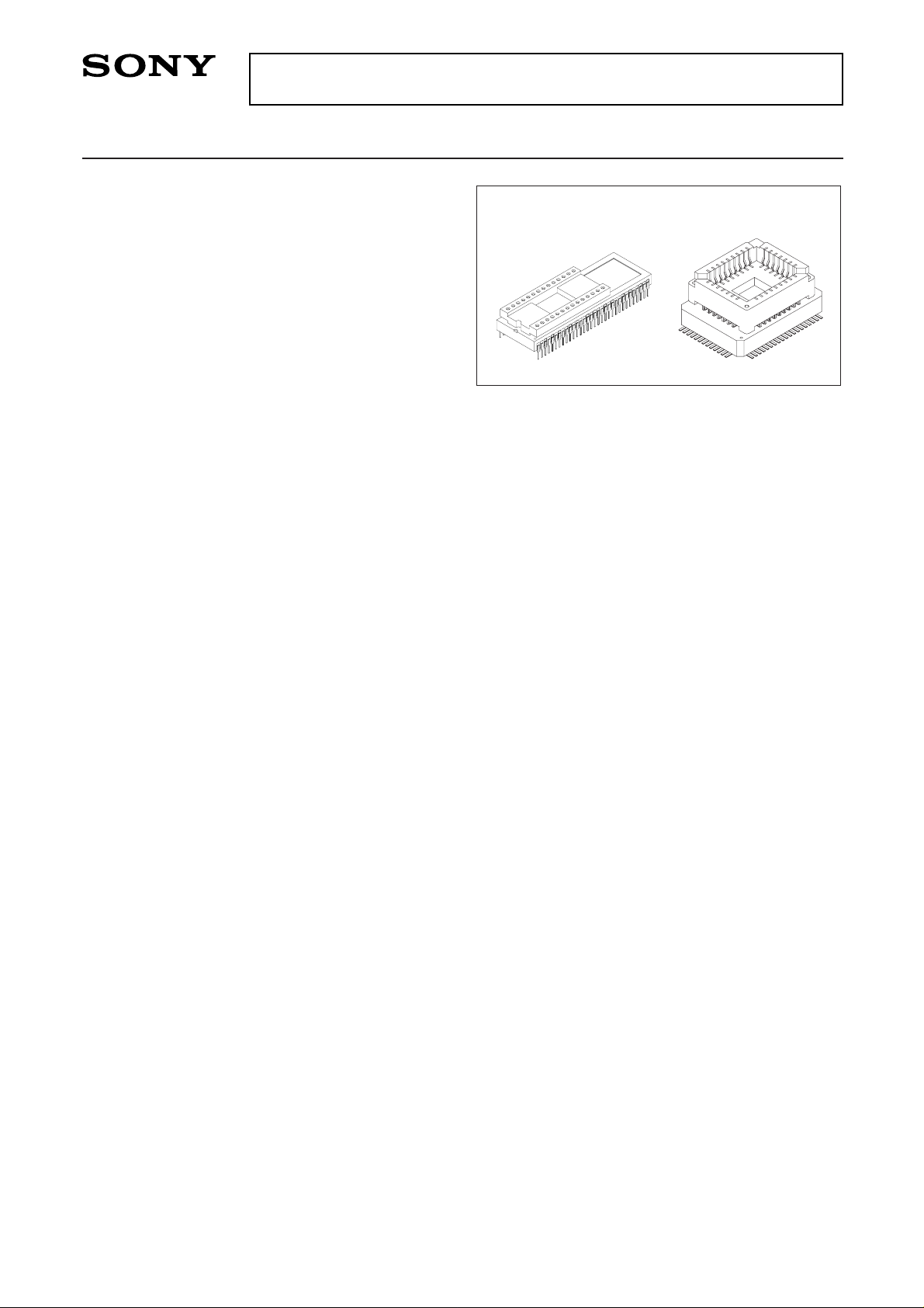
64 pin PSDIP (Ceramic) 64 pin PQFP (Ceramic)
Piggyback/
evaluator type
For the availability of this product, please contact the sales office.

– 2 –
CXP5080
ALU
VL
VLC1
EXTAL
SEG16
SEG23
XTAL
V
LC3
VLC2
13
8
Accumulator
Flag
Timer (8)
Timer/counter (8)
Serial I/O (8)
Register
Data memory
Stack
Data memory
Interruption control
Port A Port B Port C Port D Port E Port F
(Enables to specify
the I/O with bit unit)
(Enables to specify
the I/O with port unit)
(Combined use of mask
with segment output, optional.)
Program
counter (13)
A0 to A12
I0 to I7
Time base timer (18)
LCD
controller/driver
Instruction
input buffer
400 × 4
bits
Address buffer
Clock control
Instruction control
Port YPort X
(Combined use of serial I/O)
16 4
to to to
SEG0
SEG15
COM0
COM3
PX3/SI
PX2/SOA
PX1/SOB
PX0/SC
PX3/EC
PY2/INT2
PY1
PY0
INT1
V
DD
WP
VSS
RST
4
4 44
8
Block Diagram
 Loading...