

Sony CXP5078, CXP5076 Datasheet

CMOS 4-bit Single Chip Microcomputer
Description
CXP5076/5078 is a CMOS 4-bit microcomputer
which consists of 4-bit CPU, ROM, RAM, I/O port,
8-bit timer, 8-bit timer/counter, 18-bit time base
timer, 8-bit serial I/O, vector interruption, power on
reset function, liquid crystal displayer (LCD)
controller/driver, D/A conversion 14-bit PWM output
port, a remote control reception circuit with noise
eliminating circuit, 3-bit A/D converters, a 32kHz
timer/event counter and a power supply voltage
detection reset function. They are integrated into a
single chip with the standby function, etc. which are
to be operated at a low power consumption.
Features
• Instruction cycle 1.9µs/4.19MHz
122 µs/32kHz
(Possible to select with the program)
• ROM capacity 8192 × 8 bits (CXP5078)
6144 × 8 bits (CXP5076)
• RAM capacity 448 × 4 bits (Including stack, display area)
• 43 general purpose I/O ports
• 8 high current output ports
• LCD controller/driver (Possible to direct drive)
— Possible to select with the program the segment output of 16 to 32
— Possible to select with the program the duty of static, 1/2, 1/3 and 1/4
— Possible to select with the program the bias of 1/2, 1/3
• 14-bit PWM output for D/A conversion
• Remote control reception circuit
• 3-bit A/D converter (8 channels per circuit)
• 32kHz timer/event counter
• Power supply voltage detection reset function
• Low voltage operation (2.5V) ..... when operating in 122µs/32kHz
• Rich wake-up function
• 8-bit/4-bit variable serial I/O
• Arithmetic and logical operations possible between the entire ROM area, I/O area and the accumulator by
means of the memory mapped I/O
• 8-bit timer, 8-bit timer/event counter and 18-bit time base timer, independently controlled
• 2 kinds of power down modes of sleep and stop
• Power on reset circuit (mask option)
• Provided with 80 pin plastic QFP
• Provided with 80 pin piggyback QFP (CXP5070)
Structure
Silicon gate CMOS IC
– 1 –
E88037A78-PS
Sony reserves the right to change products and specifications without prior notice. This information does not convey any license by
any implication or otherwise under any patents or other right. Application circuits shown, if any, are typical examples illustrating the
operation of the devices. Sony cannot assume responsibility for any problems arising out of the use of these circuits.
CXP5076/5078
80 pin QFP (Plastic)
For the availability of this product, please contact the sales office.
– 2 –
CXP5076/5078
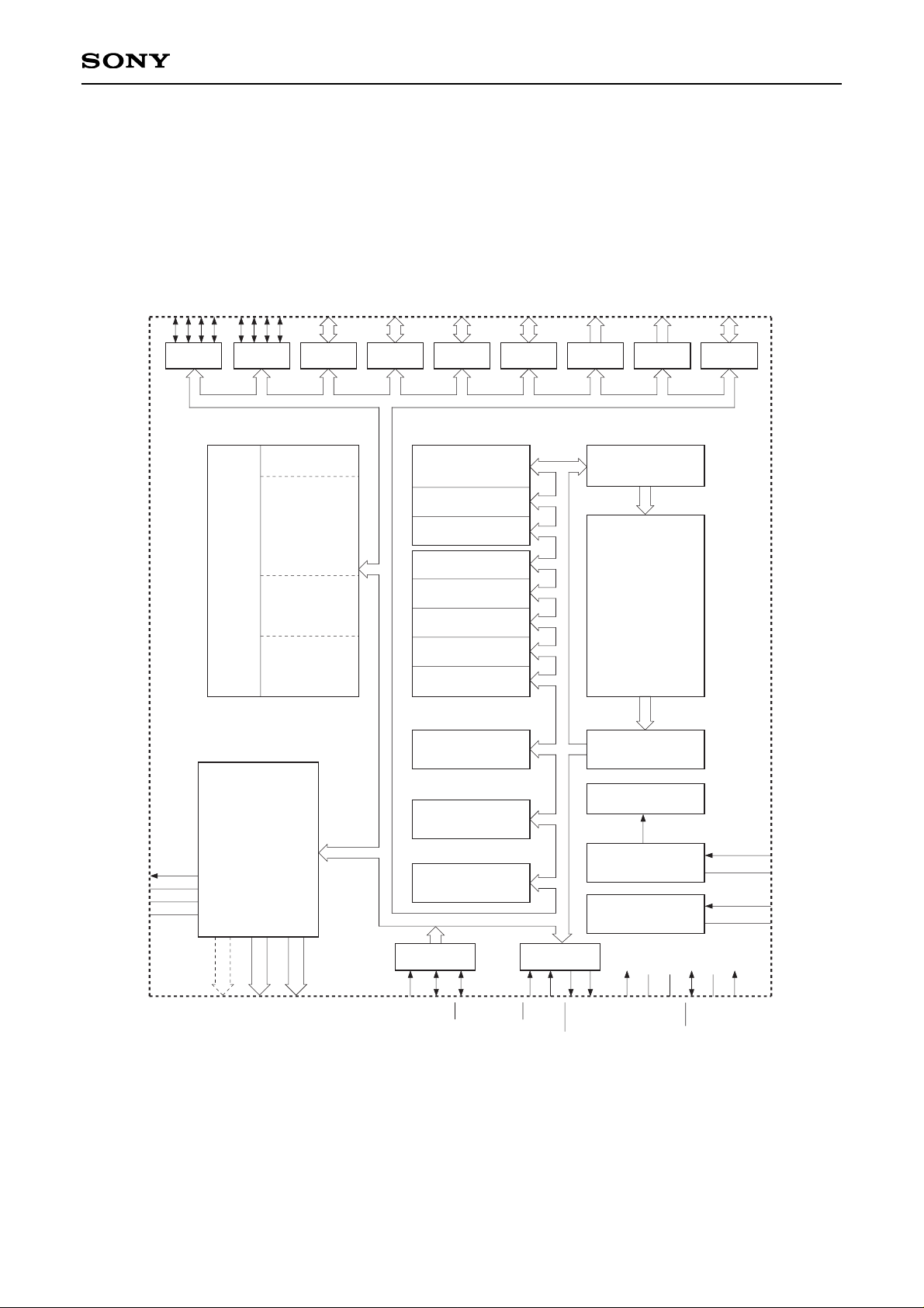
Block Diagram
PORT A PORT B PORT C PORT D PORT E PORT F PORT G PORT H PORT I
44 44
(Common with A/D
converter analog input)
(Input and output is
possible by bit unit)
(Common with segment
output S27 to S24)
(Common with segment
output S31 to S28)
(Common with segment
output S19 to S16)
(Common with segment
output S23 to S20)
(Common with A/D
converter analog input)
(Input and output is
possible by port unit)
44 4
(Input and output is
possible by port unit)
448 × 4
bits
Resister
Data memory
Stack
Data memory
ALU
Accumulator
Flag
Timer (8)
Sub time (8)
Timer/Counter (8)
Serial I/O (8)
Interrupt control
Program
counter (13)
Program
memory
8192 × 8 bits
(CXP5078)
8144 × 8 bits
(CXP5076)
PWM (14)
A/D Converter
Remote control
receiving
Instruction control
Time base timer (18)
Clock control
32kHz timer/
event counter
Port X Port Y
LCD controller/
driver
16 16 4
VL
VLC1
VLC2
VLC3
EXTAL
XTAL
TEX
TX
(Common with serial I/O)
(Common with
port C, port D,
port G, port H)
SEG16 to SEG31
SEG0 to SEG15
COM0 to COM3
PX2/SI
PX1/SO
PX0/SC
PY3/EC
PY2/WP
PY1/PWM
PY0
INT
V
DD
V
SS
RST
V
REF
RMC

– 3 –
CXP5076/5078
Pin Configuration (Top View)
PG1/SEG18
PG2/SEG17
PG3/SEG16
SEG15
SEG14
SEG13
SEG12
SEG11
SEG10
SEG9
SEG8
SEG7
SEG6
SEG5
SEG4
SEG3
SEG2
SEG1
SEG0
COM3
COM2
COM1
COM0
V
LC1
PD1/SEG30
PD0/SEG31
PY3/EC
PY2/WP
PE2
PE1
PE0
PF3
PF2
PF1
PF0
PA3
PA1
PA0
PX2/SI
PX1/SO
PX0/SC
NC
PB3/AD7
PB2/AD6
V
LC2
V
LC3
V
L
RMC
INT
XTAL
EXTAL
RST
NC
V
DD
AD0/PI0
AD1/PI1
AD2/PI2
AD3/PI3
AD4/PB0
AD5/PB1
NC
PG0/SEG19
PH3/SEG20
PH1/SEG22
PH0/SEG23
V
REF
TEX
TX
V
SS
PC3/SEG24
PC2/SEG25
PC1/SEG26
PC0/SEG27
PD3/SEG28
PD2/SEG29
40
39
38
37
36
35
34
31
32
33
41
42
43
44
45
46
47
48
49
50
51
52
53
54
55
56
57
58
59
60
70
69
68
67
63
64
65
66
61
62
71
72
73
74
75
76
77
78
79
80
2
3
4
5
6
7
8
9
10
11
12
13
14
15
16
17
18
19
20
21
22
23
24
25
26
27
28
29
30
1
PA2
PY0
PE3
PY1/PWM
PH2/SEG21
Note) Do not make any connections to NC pins.
– 4 –
CXP5076/5078
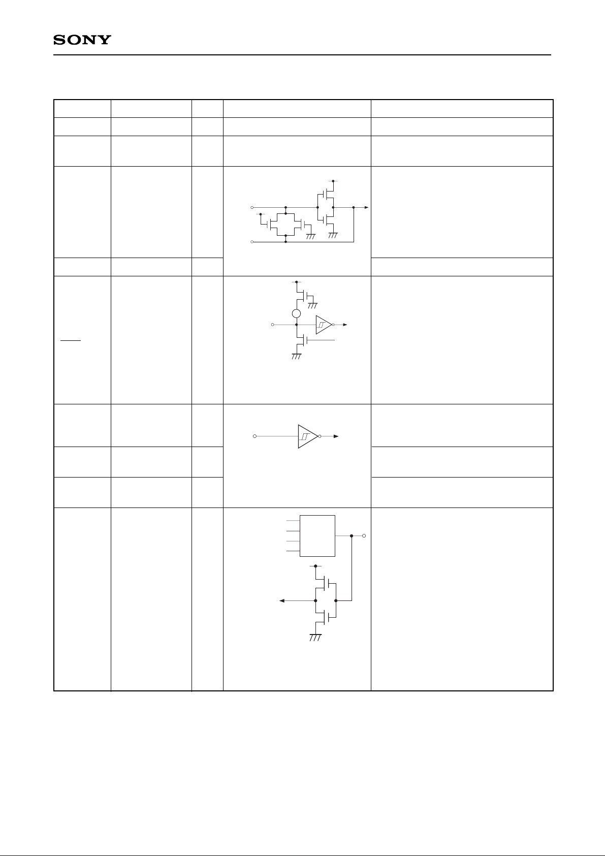
Pin Description
Symbol Name I/O Equivalent Circuit Description
Supply voltage
Grounding
voltage
Clock input
Clock output
Reset
External
interrupt
Remote control
input
Port X2
Serial input
Port X1
Serial output
—
—
I
O
I/O
I
I
I
I/O
Positive voltage supply pin
GND pin
Clock oscillation circuit input pin.
Connect the crystal oscillator or
ceramic resonator between the EXTAL
and XTAL. When using as the
external clock input, connect the clock
oscillation source to the EXTAL pin
and open the XTAL pin.
Clock oscillation circuit output pin
Serves as the incorporated power-on
reset circuit output pin.
When inputting a reset signal from the
outside, provide 2 instruction cycles or
longer of an "L" level (0V).
Serves the interrupt input pin.
Permits the selection with a program
of the edge and the level modes.
Remote control receiver input pin
Doubles as a serial interface (8 bits)
input pin and as bit "2" (input) of port X.
Doubles as a serial interface (8 bits)
output pin and as bit "1" (input) of
port X. (SO output possible to inhibit
with the program.)
EXTAL
XTAL
P
N
PN
P
N
E
Mask option
(Note 2)
Data
Output Select
Disable
Standby
P
N
(Only during
tri-state output)
VDD
VSS
EXTAL
XTAL
RST
INT
RMC
PX2/SI
PX1/SO
Output pull-up resistor (P-ch Tr)
N-ch Tr output
Schmitt inverter input
See Note 2) for the output
circuit format.
Inverter input
Schmitt inverter input
– 5 –
CXP5076/5078
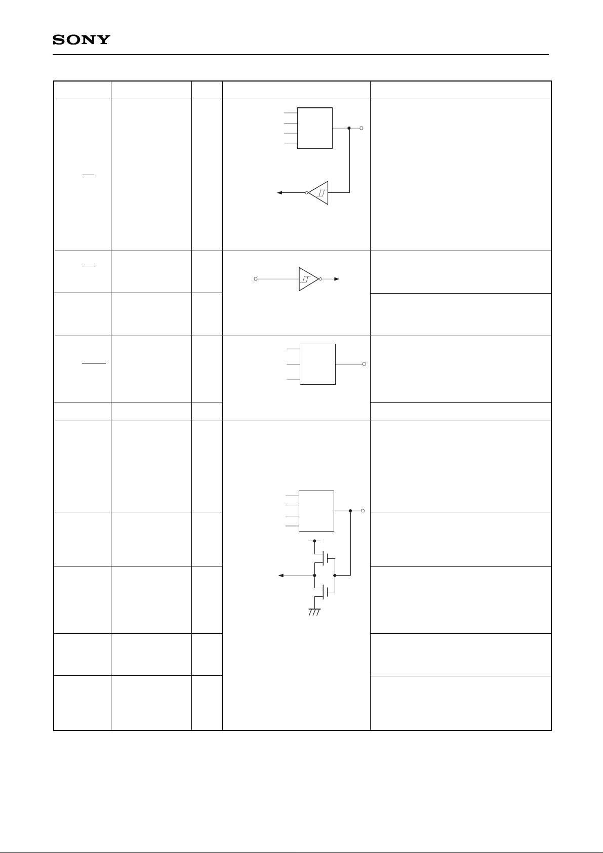
Symbol Name I/O Equivalent Circuit Description
Port X0
Serial clock
Port Y3
Event count
input
Port Y2
Wake-up
input
Port Y1
PWM
generator
output
Port Y0
Port A
Port B
Analog voltage
input
Port E
Port F
Port I
Analog voltage
input
I/O
I
I
O
O
I/O
I/O
I/O
I/O
I/O
(Note 2)
Data
Output Select
Disable
Standby
(Only during
tri-state output)
PX0/SC
PY3/EC
PY2/WP
PY1/PWM
PY0
PA0
to
PA3
PB0/AD4
to
PB3/AD7
PE0
to
PE3
PF0
to
PF3
PI0/AD0
to
PI3/AD3
See Note 2) for the output
circuit format.
Schmitt inverter input
(Note 2)
Data
Output Select
Disable
Standby
P
N
(Only during
tri-state output)
See Note 2) for the output
circuit format.
Inverter input
See Note 1) for the output
circuit format.
Schmitt inverter input
Doubles as shift clock input/output pin
for the serial interface and as bit "0"
(input) of port X.
Doubles as event counter (8 bits) input
pin and as bit "3" (input) of port Y.
Doubles as wake-up input pin to
release the standby state and as bit
"2" (input) of port Y.
Doubles as PWM generator (14 bits)
output pin and as bit "1" (output) of
port Y.
Output pin for bit "0" of port Y.
This 4-bit input/output port permits its
each individual bit to be programmed
to serve either as input or output. For
the output format, a tri-state and pullup resistor possible to be programmed,
and it is also used as the standby
resetting pin.
This 4-bit input/output port has the
functions that are equivalent to those
of port A. It is also used for A/D
converter input.
This 4-bit input/output port permits its
each individual port to be programmed
to serve either as input or output. For
the output format, a tri-state and pullup resistor possible to be programmed.
This 4-bit input/output port has the
functions that are equivalent to those
of port E.
This 4-bit input/output port has the
functions that are equivalent to those
of port E.
It is also used for A/D converter input.
(Note 1)
Data
Output Select
Disable
– 6 –
CXP5076/5078
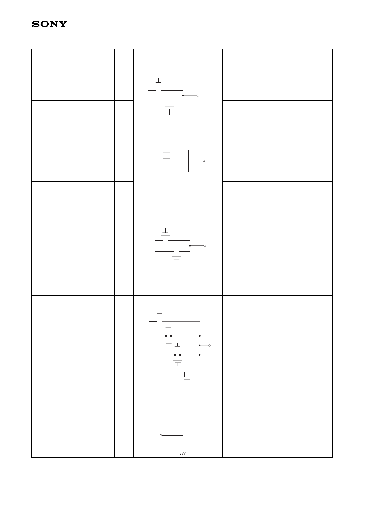
Symbol Name I/O Equivalent Circuit Description
Port D
Segment
output
Port C
Segment
output
Port H
Segment
output
Port G
Segment
output
Segment
output
Common
output
Power supply
for LCD
Cut-off
output
O
O
O
O
O
O
—
O
Doubles as a 4-bit output port (For the
output format, the inverter and pull-up
resistor possible to be programmed.)
and as the segment signal output pin
for LCD.
Doubles as a 4-bit output port (The
output format is equivalent to port D.)
and as the segment signal output pin
for LCD.
Doubles as a 4-bit output port (The
output format is equivalent to port D.)
and as the segment signal output pin
for LCD. (Possible to designate in bit
units.)
Doubles as a 4-bit output port (The
output format is equivalent to port D.)
and as the segment signal output pin
for LCD.
Segment signal output pin for LCD
Common signal output pin for LCD
Bias power supply pin for LCD
Control pin which cuts off the current
input to the bias resistor for the
external LCD during standby.
P
N
Segment
(Note 3)
Data
Output Select
Standby
Port C, D, G, H
LCD/PORT
select
P
N
P
N
PD3/
SEG31
to
PD0/
SEG28
PC3/
SEG27
to
PC0/
SEG24
PH3/
SEG23
to
PH0/
SEG20
PG3/
SEG19
to
PG0/
SEG16
SEG0
to
SEG15
COM0
to
COM3
VLC1
to
VLC3
VL
The transfer gate input signal
is controlled based on 1/2, 1/3
bias method in advance.
See Note 3) for the output
circuit format.
Transfer gate output
The transfer gate input signal
is controlled based on 1/2, 1/3
bias methods in advance.
N
 Loading...