

Sony CXP402 Datasheet
CMOS 4-bit Single Chip Microcomputer
Description
The CXP402 is a CMOS 4-bit single chip microcomputer which consists of 4-bit CPU, ROM, RAM,
8-bit timer, 8-bit timer/counter, 18-bit time-base timer,
LCD controller/driver, digital signal processor circuit
for CD player, 1-bit DAC and the like.
Features
• Instruction cycle 1.89µs for 16.93MHz oscillation
• ROM capacity 6144 × 8 bits
• RAM capacity 400 × 4 bits
(Including stack and display area)
• LCD controller/driver (Enables to direct drive)
• 8-bit timer, 8-bit timer/event counter and 18-bit
time-base timer are incorporated; they are
independently controllable.
• Arithmetic and logical operations between the entire
RAM area, I/O area and the accumulator by means
of the memory mapped I/O.
• Entire ROM area can be referred by the table look-
up instruction.
Digital Signal Processor (DSP) Block
• Playback mode supporting CAV (Constant Angular
Velocity)
• Frame jitter free
• Allows relative rotational velocity readout
• Supports spindle external control
• Wide capture range playback mode
• Spindle rotational velocity following method
• 16K RAM
• EFM data demodulation
• Enhanced EFM frame sync signal protection
• SEC strategy-based error correction
• Subcode demodulation and Sub Q data error
detection
• Digital spindle servo
• 16-bit traverse counter
• Asymmetry correction circuit
• Servo auto sequencer
• Digital audio interface output
• Digital peak meter
Digital Filter, DAC and Analog Low-Pass Filter Blocks
• DBB (digital bass boost) function
• Digital de-emphasis
• Digital attenuation
• Zero detection function
• 8Fs oversampling digital filter
• S/N: 100dB or more
(master clock: 384Fs, typ.)
Logical value: 109dB
• THD + N: 0.007% or less
(master clock: 384Fs, typ.)
• Rejection band attenuation: –60dB or more
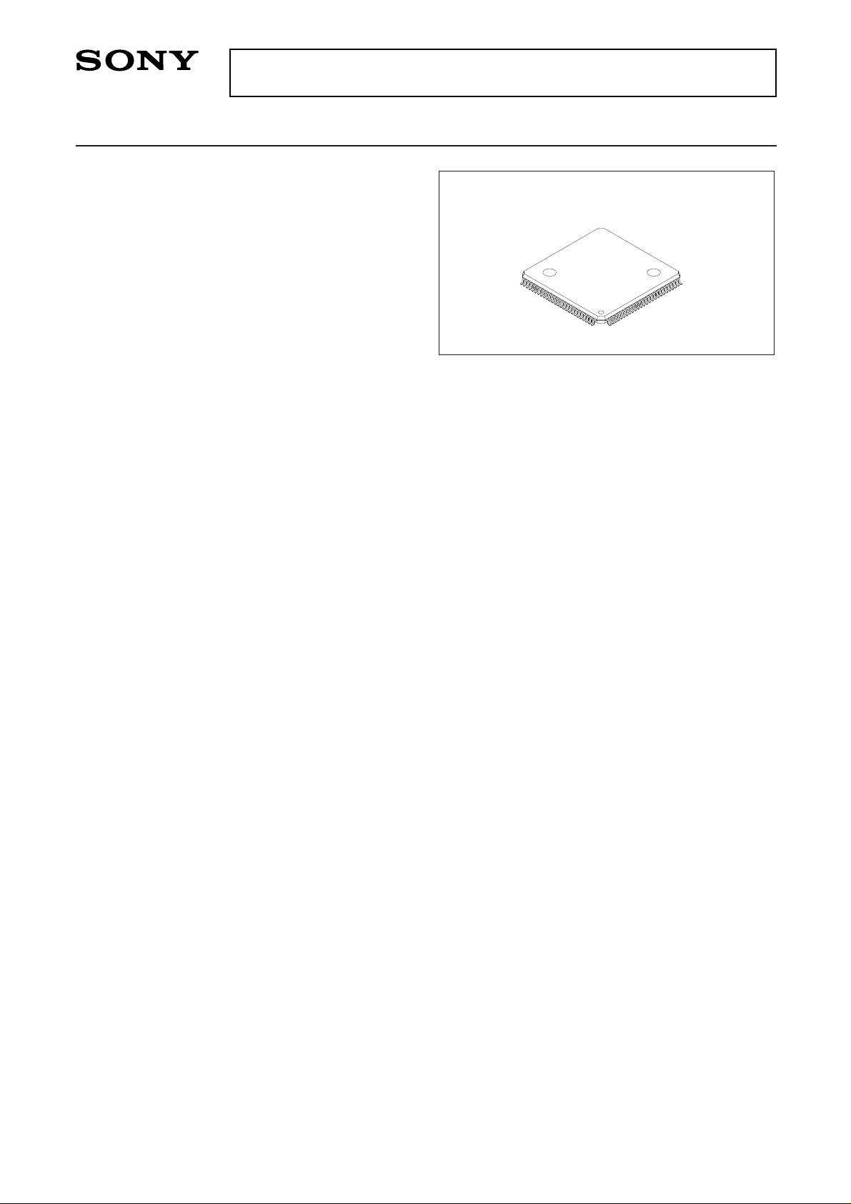
• 112-pin plastic LQFP
• Piggyback package (CXP401Z) available
Structure
Silicon gate CMOS IC
– 1 –
E98924-PS
Sony reserves the right to change products and specifications without prior notice. This information does not convey any license by
any implication or otherwise under any patents or other right. Application circuits shown, if any, are typical examples illustrating the
operation of the devices. Sony cannot assume responsibility for any problems arising out of the use of these circuits.
CXP402
112 pin LQFP (Plastic)
For the availability of this product, please contact the sales office.

– 2 –
CXP402
58
59
60
63
64
61
62
70
65
XRST
RMC
PC3
PC2
PC1
PC0
PB3
PB2
PB1
PB0
29
SEIN
CNIN
DATO
XLTO
CLKO
MON
MDS
MDP
LOCK
VPCO2
VPCO1
VCKI
V16M
VCTL
PCO
FILI
FILO
AV
SS
CLTV
AV
DD
RF
BIAS
ASYI
ASYO
C4M
SBSO
EXCK
8
9
10
11
12
13
14 15
16
17
18
19
20
21
22
23
24
25
26
2
3
4
5
1
49
54
55
V
LC1
V
LC2
V
LC3
COM0
COM1
COM2
COM3
SEG0
SEG1
SEG2
SEG3
88
87
86
85
89
90
95
94
91
92
93
LRCK
PCMD
PCMDI
BCK
BCKI
AV
SS
AV
DD
AOUT2
AIN2
LOUT2
AV
SS
XV
SS
XTAO
XTAI
XV
DD
AV
SS
LOUT1
AIN1
AOUT1
AV
DD
AV
SS
LRCKI
37
36
35
34
32
33
100
99
98
97
96
101
102
103
104
105
106
107
108
109
110
111
69
68
67
66
PA3
PA2
PA1
PA0
73
74
81
82
83
84
75
76
77
78
79
80
SEG15
SEG14
SEG13
SEG12
SEG11
SEG10
SEG9
SEG8
SEG7
SEG6
SEG5
SEG4
27
28
TEST1
TEST0
GTOP
XPCK
RFCK
C2PO
XROF
MNT3
MNT1
MNT0
DOUT
WFCK
39
38
41
42
45
46
47
48
50
52
6
7
57
71
72
V
SS
VDD
VDD
VSS
43
44
56
CTEST
DTEST
V
SS
VDD
XRSTO
FOK
GFS
EMPH
SCOR
30
31
51
53
40
LCD Controller/Driver
SPC500
CPU Core
ROM
6K Byte
RAM
400 × 4bit
T/C RMC
Port RST
SCOR
EMPHI
Servo Auto
Sequencer
Digital
CLV
Digital
PLL
Asymmetry
Collector
D/A
I/F
EFM
Demodulator
EPROM
Collector
1-bit DAC
Digital Filter
Test
Circuit
Analog
Out
16K
RAM
ACDT
RMUT
LMUT
DATA
XLAT
CLOK
XRST
SYSM
PWMI
XTSL
ASYE
SENS
FOK
GFS
SQCK
SQSO
INT
PY0
PY2
PX0
PX3
PF0
PF1
PF2
PF3
PE0
PE1
PE2
PE3
PD0
PD1
PD2
PY1
SIO I/F
OSC
PORT I/F CPU I/F
PY3
Block Diagram

– 3 –
CXP402
Pin Configuration (Top View)
2
3
4
5
6
7
8
9
10
11
12
13
14
15
16
17
18
19
20
21
22
23
24
25
26
27
28
1
57
58
59
60
63
64
61
62
70
69
68
67
65
66
71
72
73
74
81
82
83
84
75
76
77
78
79
80
SEIN
CNIN
DATO
XLTO
CLKO
V
SS
VDD
MON
MDP
MDS
LOCK
VPCO2
VPCO1
VCKI
V16M
VCTL
PCO
FILI
FILO
AV
SS
CLTV
AV
DD
RF
BIAS
ASYI
ASYO
TEST1
TEST0
XRST
XRSTO
FOK
LRCK
PCMD
PCMDI
BCK
BCKI
GTOP
XPCK
GFS
RFCK
C2PO
V
SS
V
DD
XROF
MNT3
MNT1
MNT0
C4M
DOUT
EMPH
WFCK
SCOR
SBSO
EXCK
DTEST
NC
AV
SS
AV
DD
AOUT2
AIN2
LOUT2
AV
SS
XV
SS
XTAO
XTAI
XV
DD
AV
SS
LOUT1
AIN1
AOUT1
AV
DD
AV
SS
V
LC1
V
LC2
V
LC3
COM0
COM1
COM2
COM3
SEG0
SEG1
SEG2
SEG3
SEG15
V
DD
VSS
RMC
PC3
PC2
PC1
PC0
CTEST
PB3
PB2
PB1
PB0
PA3
PA2
PA1
PA0
SEG14
SEG13
SEG12
SEG11
SEG10
SEG9
SEG8
SEG7
SEG6
SEG5
SEG4
LRCKI
88
87
86
85
89
90
100
99
98
97
96
95
94
91
92
93
101
102
103
104
105
106
107
108
109
110
111
112
29
30
40
39
38
37
36
35
34
31
32
33
41
42
43
44
45
46
47
48
49
50
51
52
53
54
55
56
– 4 –
CXP402
Pin Description
Symbol
I/O
Description
(Port A)
4-bit I/O port. I/O can be set in a unit of single bits. Pull-up resistor is
attached for input. (4 pins)
(Port B)
4-bit I/O port. I/O can be set in a unit of single bits. Pull-up resistor is
attached for input. (4 pins)
(Port C)
4-bit I/O port. I/O can be set in a unit of single bits. Pull-up resistor is
attached for input. (4 pins)
LCD segment signal output. (16 pins)
LCD common signal output.
LCD bias power supply. Bias voltage is generated, which is 1/3 the
supply voltage due to the internal resistor. (3 pins)
SENS input from SSP.
Track jump count signal input.
Serial data output to SSP.
Serial data latch output to SSP.
Serial clock output to SSP.
Spindle motor ON/OFF control output.
Spindle motor servo control. (2 pins)
Lock signal output. GFS is sampled at 460Hz and; when GFS is high,
this pin outputs a high signal. If GFS is low eight convective samples,
this pin outputs low.
Wide-band EFM PLL charge pump output. (2 pins)
Wide-band EFM PLL VCO2 oscillation input.
Wide-band EFM PLL VCO2 oscillation output.
Wide-band EFM PLL VCO2 control voltage input.
Master PLL charge pump output.
Master PLL filter input.
Master PLL filter output.
Master VCO control voltage input.
EFM signal input.
Asymmetry circuit constant current input.
Asymmetry comparator voltage input.
EFM output. (full swing)
System reset input. Active at low.
I/O
I/O
I/O
Output
Output
Input
Input
Output
Output
Output
Output
Output
(tri-state)
Output
Output
(tri-state)
Input
Output
Input
Output (tri-state)
Input
Output (Analog)
Input
Input
Input
Input
Output
Input
PA0 to PA3
PB0 to PB3
PC0 to PC3
SEG0 to SEG15
COM0 to COM3
VLC1 to VLC3
SEIN
CNIN
DATO
XLTO
CLKO
MON
MDP
MDS
LOCK
VPCO1
VPCO2
VCKI
V16M
VCTL
PCO
FILI
FILO
CLTV
RF
BIAS
ASYI
ASYO
XRST
CXP402
Symbol
I/O
Description
Reset signal output. Active at low.
Focus OK input.
Used for SENS output and servo auto sequencer.
D/A interface LR clock output. (f = Fs)
LR clock input.
D/A interface serial data output.
D/A interface serial data input.
D/A interface bit clock output.
D/A interface bit clock input.
GTOP output.
XPLCK output.
GFS output.
RFCK output.
C2PO output.
XRAOF output.
MNT3 output.
MNT1 output.
MNT0 output.
1/4 frequency division output of the oscillation input. (4.2336MHz for
16.3944MHz)
Digital Out output.
De-emphasis ON/OFF output. High is output for ON; low is output for OFF.
WFCK output.
Subcode sync detection output. Outputs a high signal when either
subcode sync S0 or S1 is detected.
Sub P to W serial data output.
SBSO serial clock input.
Lch analog output.
Lch operational amplifier input.
Lch LINE output.
Rch analog output.
Rch operational amplifier
Rch LINE output.
Remote control receiver circuit input.
Connect a crystal for system clock oscillation. When the clock is supplied
externally, input it to the XTAI pin and leave the XTAO pin open.
No connected.
Output
Input
Output
Input
Output
Input
Output
Input
Output
Output
Output
Output
Output
Output
Output
Output
Output
Output
Output
Output
Output
Output
Output
Input
Output (Analog)
Input (Analog)
Output
Output (Analog)
Input (Analog)
Output
Input
Input
XRSTO
FOK
LRCK
LRCKI
PCMD
PCMDI
BCK
BCKI
GTOP
XPCK
GFS
RFCK
C2PO
XROF
MNT3
MNT1
MNT0
C4M
DOUT
EMPH
WFCK
SCOR
SBSO
EXCK
AOUT1
AIN1
LOUT1
AOUT2
AIN2
LOUT2
RMC
XTAI
XTAO
NC
– 5 –
 Loading...