

Sony CXL5502P, CXL5502M Datasheet
CMOS-CCD 1H Delay Line for NTSC
Description
The CXL5502M/N/P are CMOS-CCD delay line ICs
that provide 1H delay time for NTSC signals including
the external low-pass filter.
The ICs contain a PLL circuit (quadruple progression).
Features
• Single power supply (5V)
• Low power consumption 95mW (Typ.)
• Built-in peripheral circuits
• Clamp level of I/O signal can be selected
• Built-in quadruple PLL circuit
Functions
• 905-bit CCD register
• Clock driver
• Autobias circuit
• Input clamp circuit
• Sample and hold circuit
• PLL circuit (quadruple progression)
Structure
CMOS-CCD
Absolute Maximum Ratings (Ta = 25°C)
• Supply voltage VDD 6V
•Operating temperature Topr –10 to +60 °C
• Storage temperature Tstg –55 to +150 °C
• Allowable power dissipation
PD
CXL5502M 400 mW
CXL5502N 260 mW
CXL5502P 800 mW
Recommended Operating Condition (Ta = 25°C)
Supply voltage VDD 5 ± 5% V
Recommended Clock Conditions (Ta = 25°C)
• Input clock amplitude VCLK 0.3 to 1.0 Vp-p
(0.5Vp-p typ.)
• Clock frequency fCLK 3.579545 MHz
• Input clock waveform Sine wave
Input Signal Amplitude
VSIG 500mVp-p (Typ.), 572mVp-p (Max.)
(at internal clamp condition)
– 1 –
E89930E79-PS
Sony reserves the right to change products and specifications without prior notice. This information does not convey any license by
any implication or otherwise under any patents or other right. Application circuits shown, if any, are typical examples illustrating the
operation of the devices. Sony cannot assume responsibility for any problems arising out of the use of these circuits.
CXL5502M/N/P
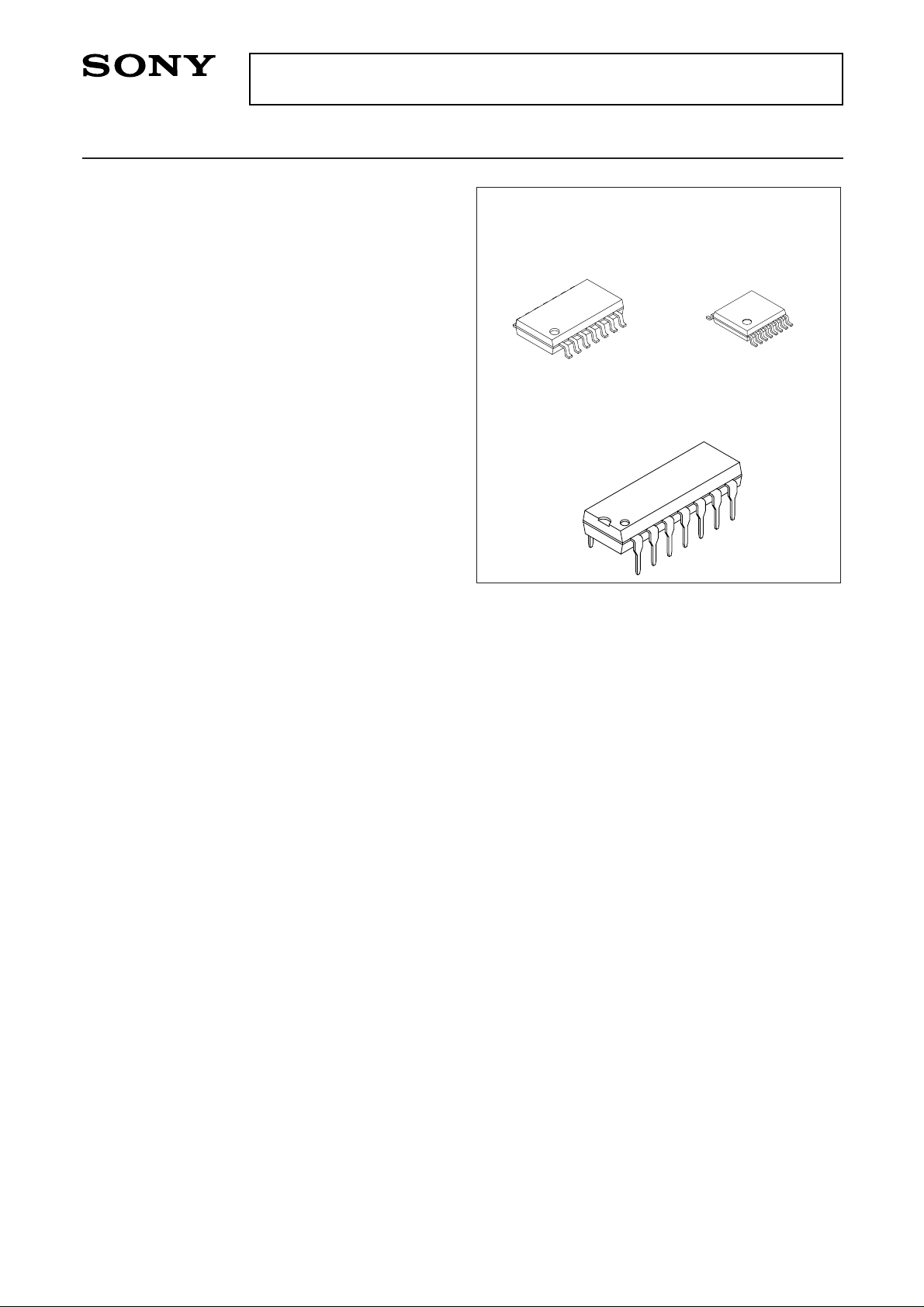
CXL5502M
14 pin SOP (Plastic)
CXL5502N
16 pin SSOP (Plastic)
CXL5502P
14 pin DIP (Plastic)
For the availability of this product, please contact the sales office.
– 2 –
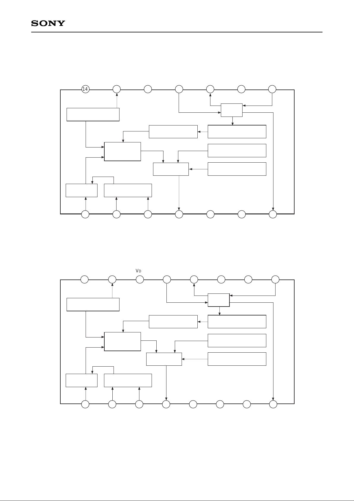
CXL5502M/N/P
Autobias circuit
Clock driver
Bias circuit (A)
Bias circuit (B)
PLL
Timing circuit
CCD
(905bit)
Clamp circuit
Output circuit
(S/H 1bit)
14
V
SS
12
V
DD
11
VCO
IN
10
PC
OUT
9
V
DD
8
CLK
1
IN
2
I/O1
3
I/O2
4
OUT
5
V
SS
7
VCO
OUT
6
V
SS
I/O control
13
AB
14
VDD
12
PC
OUT
11
(N.C)
10
V
DD
9
CLK
8
VCO
OUT
1
IN
2
I/O1
3
I/O2
4
OUT
5
V
SS
7
V
SS
6
(N.C)
13
VCO
OUT
15
AB
16
V
SS
Block Diagram and Pin Configuration (Top View)
CXL5502M/P
CXL5502N
Autobias circuit
Clock driver
Bias circuit (A)
Bias circuit (B)
PLL
Timing circuit
CCD
(905bit)
Clamp circuit
Output circuit
(S/H 1bit)
I/O control

– 3 –
CXL5502M/N/P
Pin Description
CXL5502M/P
CXL5502N
Pin No. Symbol I/O Description Impedance
1
2
3
4
5
6
7
8
9
10
11
12
13
14
IN
I/O1
I/O2
OUT
VSS
VSS
VCO OUT
CLK
VDD
PC OUT
VCO IN
VDD
AB
VSS
I
I
I
O
—
—
O
I
—
O
I
—
O
—
Signal input
I/O control 1
I/O control 2
Signal output
GND
GND
VCO output
Clock input
Power supply (5V)
Phase comparator output
VCO input
Power supply (5V)
Autobias DC output
GND (SUB)
> 10kΩ at no clamp
40 to 500Ω
> 100kΩ
600 to 200kΩ
Pin No. Symbol I/O Description Impedance
1
2
3
4
5
6
7
8
9
10
11
12
13
14
15
16
IN
I/O1
I/O2
OUT
VSS
(N.C)
VSS
VCO OUT
CLK
VDD
(N.C)
PC OUT
VCO IN
VDD
AB
VSS
I
I
I
O
—
—
—
O
I
—
—
O
I
—
O
—
Signal input
I/O contorl 1
I/O contorl 2
Signal output
GND
—
GND
VCO output
Clock input
Power supply (5V)
—
Phase comparator output
VCO input
Power supply (5V)
Autobias DC output
GND (SUB)
> 10kΩ at no clamp
40 to 500Ω
> 100kΩ
600 to 200kΩ

– 4 –
CXL5502M/N/P
Description of Function
In the CXL5502M/N/P, the condition of I/O control pins (Pins 2 and 3) control the input signal clamp condition
and the mode of the output signal with relation to its input signal.
There are 2 modes for the I/O signal.
(1) PN mode
(Low level clamp/reverse phase output mode)
(2) NP mode
(High level clamp/positive phase output mode)
I/O Control Pin
(1) I/O1 (Pin 2)
Control of the I/O signal condition
DC open ..... Input signal is low level clamped and the output signal is inverted in relation to the input
signal. As the pin is biased to 2.5V by means of the resistance inside the IC, a decoupling
capacitor of around 1000pF is necessary.
GND ............. Input signal is high level clamped and the output signal turns into an inverted signal.
(2) I/O2 (Pin 3)
Control of the input signal clamp condition
0V ................. Internal clamp condition
5V ................. Non internal clamp condition
Center biased to approx. 2.1V by means of the IC internal resistance (several 10kΩ).
Usage in this mode is limited to APL 50% signals and in this mode, the maximum input
signal amplitude is 200mVp-p.
Clamp
level
Input waveform
Output waveform
Clamp
level
 Loading...