

Sony CXL1518M, CXL1517M Datasheet
CMOS-CCD Signal Processor
Description
The CXL1517M/1518M are CMOS-CCD signal
processors developed for CCD camera complementary
color filter array processing system.
CXL1517M
452.5-bit × 2, 453.5-bit 1H CCD delay line
CXL1518M
300.5-bit × 2, 301.5-bit 1H CCD delay line
Features
• Single 5V power supply
• Low power consumption (Typ.)
CXL1517M 120mW
CXL1518M 75mW
• Built-in peripheral circuits
• Built-in CDS (Correlated Double Sampling) circuit
Functions
• Clock driver
• Autobias circuit (Center and black)
• Pedestal clamp circuit
• CDS circuit
• Overflow prevention circuit
Absolute Maximum Ratings (Ta = 25°C)
• Supply voltage VDD 6V
•Operating temperature Topr –10 to +65 °C
• Storage temperature Tstg –55 to +150 °C
• Allowable power dissipation PD 500 mW
Recommended Operating Voltage Range (Ta = 25°C)
Supply voltage VDD 4.6 to 5.25 V
– 1 –
E91777A78-PS
Sony reserves the right to change products and specifications without prior notice. This information does not convey any license by
any implication or otherwise under any patents or other right. Application circuits shown, if any, are typical examples illustrating the
operation of the devices. Sony cannot assume responsibility for any problems arising out of the use of these circuits.
CXL1517M/1518M
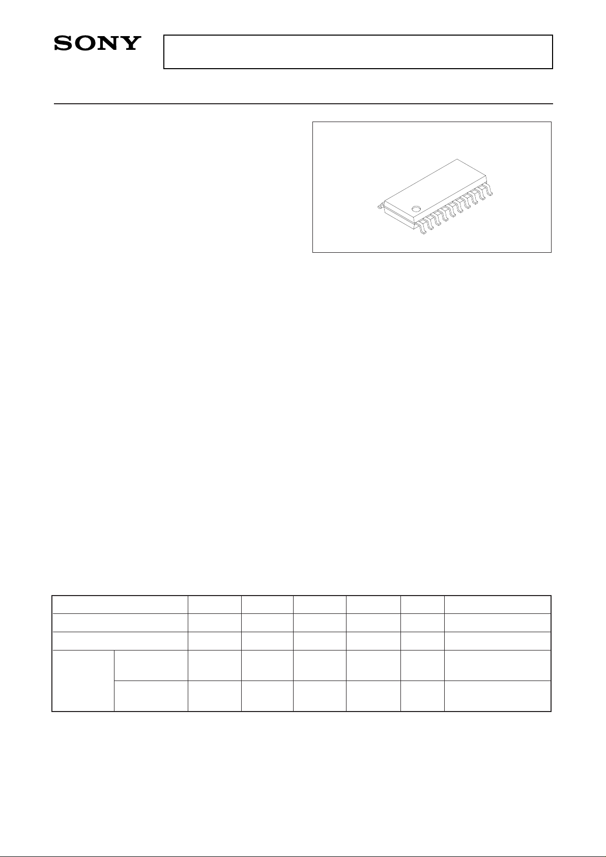
20 pin SOP (Plastic)
Structure
CMOS-CCD
Item Symbol
VL
VH
fCL
fCL
Min.
VSS
0.7 × VDD
Typ.
7.16
4.77
Max.
0.3 × VDD
VDD
Unit
V
V
MHz
MHz
Remarks
NTSC: 455fH
CCIR: 454fH
NTSC: 910fH/3
CCIR: 908fH/3
Clock voltage Low
Clock voltage High
Clock
frequency
CXL1517M
CXL1518M
– 2 –
CXL1517M/1518M
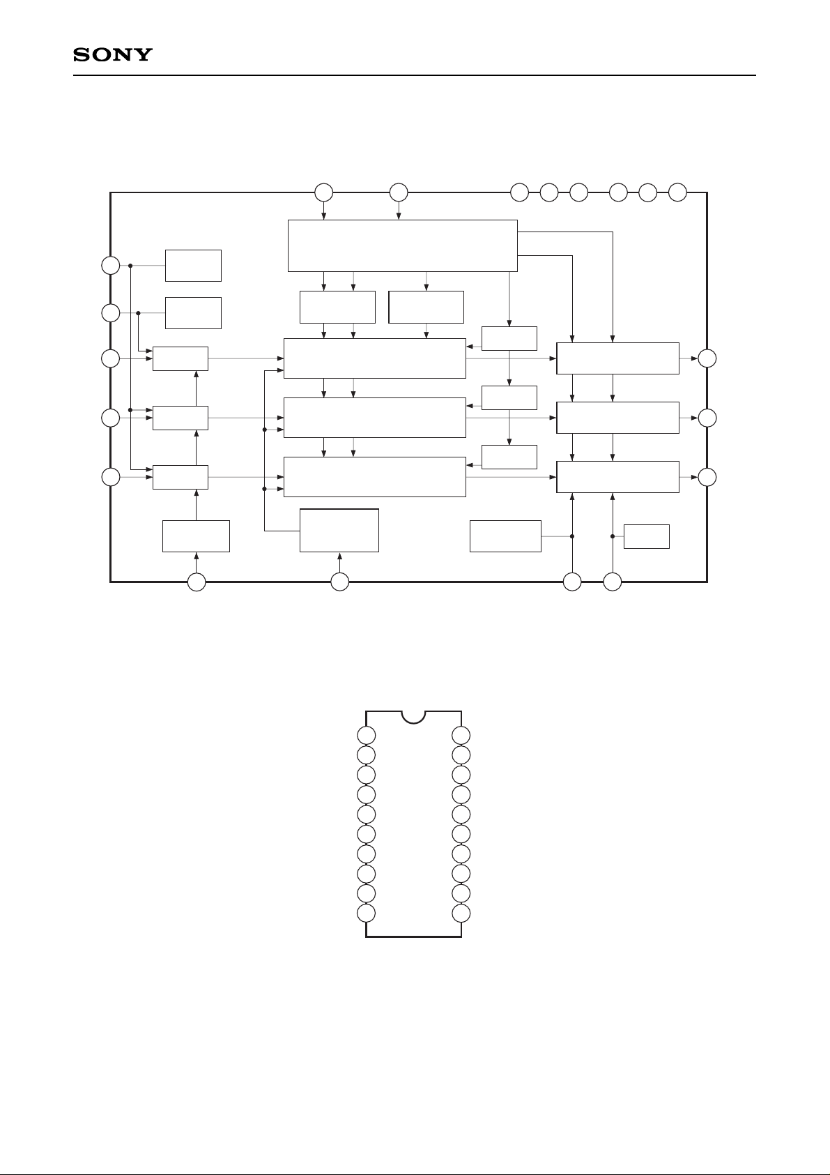
Block Diagram and Pin Configuration (Top View)
4
8
10
12
14
16
17
1
V
DD
ABCN
V
DD
ABOVF
V
DD
V
GG
IN-B
IN-A
ABBL
V
SS
XDL1
XDL2
V
SS
V
SS
CDS
CLP
A.B.
BLACK
CDS OUTPUT
CIRCUIT
CLP
DL
CDS OUTPUT
CIRCUIT
CLP
CDS OUTPUT
CIRCUIT
CLP
CLP PULSE
GEN.
OVERFLOW
PREVENTION
CIRCUIT
POTENTIAL
CONTROL
CDS
TIMING GENERATOR
9
11
13
15
OUT-C
OUT-A
OUT-B
7
2
6
IN-C
3
18
PG. GEN.
PG. GEN.
PG. GEN.
PRECHARGE
DRAIN
DRIVER
20
A.B.
CENTER
A
(n bit)
DL B
(n bit)
DL C
(n + 1 bit)
5
19
2
3
4
5
6
7
8
9
10
11
12
13
14
15
16
17
18
19
20
1
VSS
IN-B
ABBL
V
DD
IN-C
CLP
V
DD
OUT-C
V
GG
IN-A
ABCN
VDD
XDL1
XDL2
V
SS
VSS
OUT-A
CDS
ABOVF
OUT-B

– 3 –
CXL1517M/1518M
Pin Description
Pin No. Symbol I/O Description Comment
VSS
IN-B
ABBL
VDD
IN-C
CLP
VDD
OUT-C
VGG
OUT-B
OUT-A
CDS
VSS
VSS
XDL2
XDL1
VDD
ABCN
ABOVF
IN-A
—
I
O
—
I
I
—
O
O
O
O
O
—
—
I
I
—
O
O
I
GND
Signal input B channel (Y)
Autobias DC output for Y signal
Power supply
Signal input C channel (Y)
Clamp pulse input
Power supply
Signal output C channel
Output circuit bias DC output
Signal output B channel
Signal output A channel
DC output for CDS
GND
GND
Clock pulse input 2
Clock pulse input 1
Power supply
Autobias DC output for C signal
Autobias DC output for overflow prevention circuit
Signal input A channel (C)
Analog
Black level bias
Analog
Black level bias
at no clamp > 100k
> 100k
Output circuit
Output circuit
Timing
> 100k
> 100k
Timing
Center level bias
Center level bias
at no clamp > 100k
1
2
3
4
5
6
7
8
9
10
11
12
13
14
15
16
17
18
19
20
 Loading...