

Sony CXL1511M Datasheet
CCD Delay Line for PAL
For the availability of this product, please contact the sales office.
Description
The CXL1511M is an IC developed for use in
conjunction with Y/C signal processing ICs for PAL.
This CCD delay line provides the comb filter output
for eliminating the chrominance signal cross talk and
1H delay output for luminance signals.
Features
• Single power supply (5V)
• Built-in triplex progression PLL circuit
• Comb filter characteristics selectable
• Delay time for 1H delay output selectable
• Built-in peripheral circuits
• Positive phase signal input, positive phase signal
output
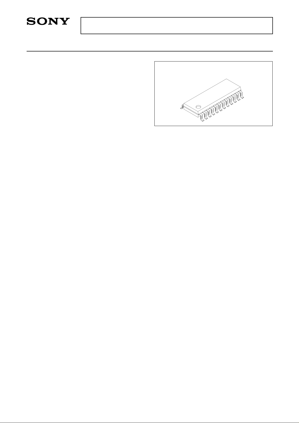
CXL1511M
24 pin SOP (Plastic)
Functions
• Comb filter output
• 1H delay output for luminance signal
• Clock driver
• Autobias circuit
• Input clamp circuit (for luminance signals)
• Center bias circuit (for chrominance signals)
• Sample-and-hold circuit
• Triplex progression PLL circuit
• Luminance signal delay time/comb filter
characteristics selection circuit
• Clock buffer output circuit
Absolute Maximum Ratings (Ta = 25°C)
• Supply voltage VDD +6 V
• Operating temperature Topr –10 to +60 °C
• Storage temperature Tstg –55 to +150°C
• Allowable power dissipation PD 500 mW
Recommended Operating Voltage (Ta = 25°C)
VDD 5V ± 5%
Structure
CMOS-CCD
Sony reserves the right to change products and specifications without prior notice. This information does not convey any license by
any implication or otherwise under any patents or other right. Application circuits shown, if any, are typical examples illustrating the
operation of the devices. Sony cannot assume responsibility for any problems arising out of the use of these circuits.
– 1 –
E95224-ST
Recommended Clock Conditions (Ta = 25°C)
• Input clock amplitude VCLK 0.3Vp-p to 1.0Vp-p (0.5Vp-p Typ.)
• Clock frequency fCLK 4.433619MHz
• Input clock waveform sine wave
Input Signal Amplitude
Vsig 350mVp-p (Typ.), 575mVp-p (Max.)
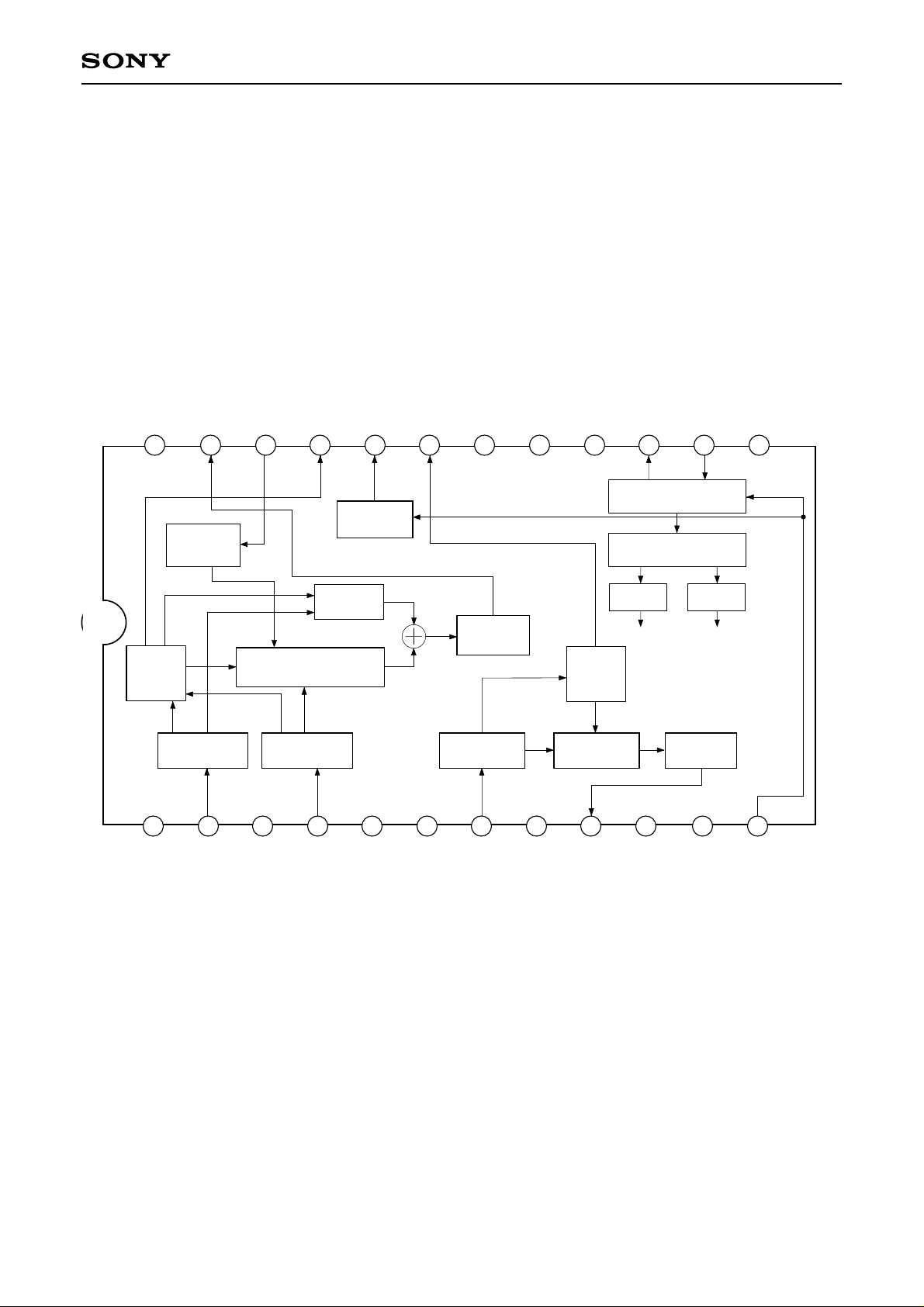
Block Diagram and Pin Configuration (Top View)
CXL1511M
Vss
24
Autobias
circuit (C)
1
Vss
C-OUT
23
Selector
Bias circuit Bias circuit
2
C-IN1
CONT
22
1H/2H + D
3
DD
V
21
4
C-IN2
AB-C
fsc
20
fsc buffer
D
5
(NC)
AB-P
19
circuit (S/H)
Clamp circuit
6
(NC)
(NC)
18
Output
7
Y-IN
17
8
(NC)
(NC)
(NC)
16
Autobias
circuit (Y)
1H
9
Y-OUT
PCOUT
PLL
Timing
Driver
φ1 φ2
Output
circuit (S/H)
10
(NC)
VCOIN
1415
Driver
11
(NC)
Vss
13
12
CLK
– 2 –
SOP 24pin
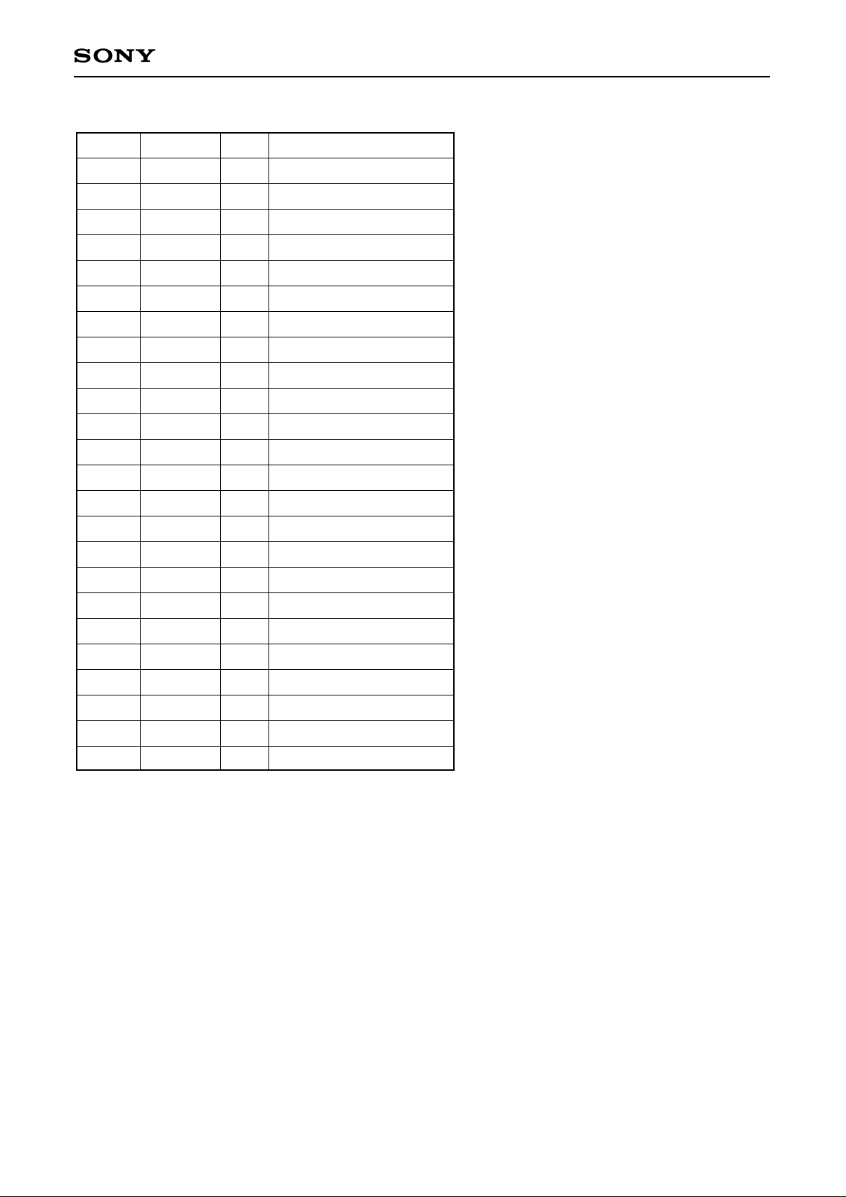
CXL1511M
Pin No.
1
2
3
4
5
6
7
8
9
10
11
12
13
14
15
16
Symbol
VSS
C-IN1
VDD
C-IN2
(NC)
(NC)
Y-IN
(NC)
Y-OUT
(NC)
(NC)
CLK
VSS
VCOIN
PCOUT
(NC)
I/O
GND
—
Chrominance signal input 1
I
Power supply
—
Chrominance signal input 2
I
Description
—
—
Luminance signal input
I
—
Luminance signal output
O
—
—
Clock input
I
GND
—
VCO input
I
Phase comparator output
O
—
—
—
—
—
—
—
17
18
19
20
21
22
23
24
(NC)
(NC)
AB-P
fsc
AB-C
CONT
C-OUT
VSS
—
—
Autobias output (P)
O
fsc buffer output
O
Autobias output (C)
O
Control input
I
Chrominance signal output
O
GND
—
—
—
– 3 –
CXL1511M
Description of Functions
The CXL1511M enables the chrominance comb filter characteristics and luminance signal delay time to be
selected in the control input state.
CONT
L
H
Mode (typical example)
PAL/GBI
4.43NTSC
Chrominance comb filter
chracteristics
2H (1702.5bit)
1H (844.5bit)
Luminance signal delay time
(number of CCD bits)
1H (848.5bit)
1H (842.5bit)
CONT Input Level
L/H
L
Min.
—
Typ.
0
Max.
0.5
Unit
V
H
2.0
5.0
6.0
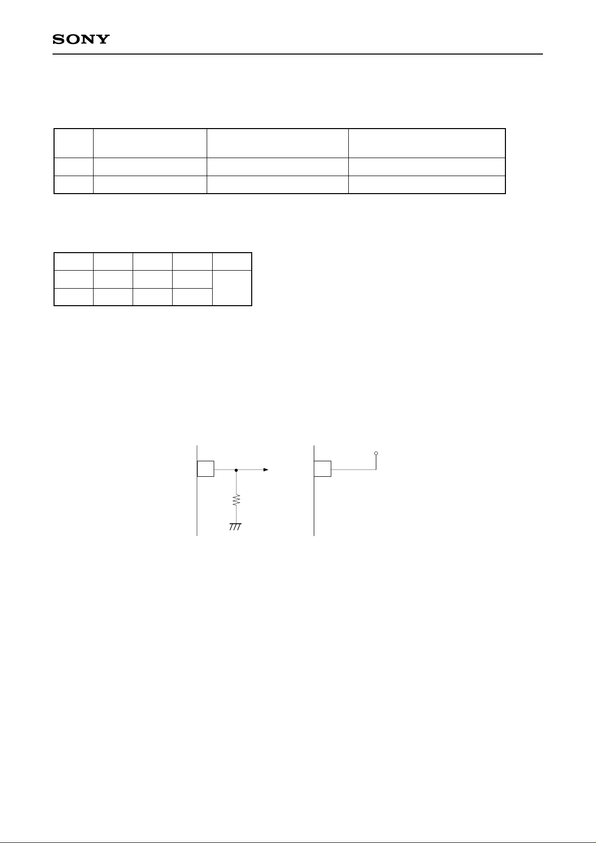
• fsc Output Pin
The buffer output of the clock input from the CLK pin is provided at the fsc output pin. Since a pull-up resistor
is contained inside the IC, the supply voltage is produced during open, and the output is stopped. Connect a
2.2kΩ pull-down resistor when the fsc output is to be used.
<When in use> <When not in use>
fsc
2.2k
fsc
VDD
– 4 –
Electrical Characteristics
(Ta = 25°C, VDD = 5V, fCLK = 4.433619MHz, VCLK = 500mVp-p sine wave)
See electrical Characteristics Measurement Circuit
CXL1511M
Item Symbol
Supply
current
IDD1
IDD2
Measurement
condition
—
1234567
bbbaaa—
bbbaba—
SW condition
Chrominance Signal Characteristics (No signals input to Y-IN)
Item Symbol
Low
frequency
gain
Frequency
response
GLC1
GLC2
FC1
FC2
LIC1
Linearity
LIC2
Comb
CCD1
depth min.
gain
CCD2
SNC1
SN ratio
SNC2
Measurement
condition
(See Note 2)
(See Note 3)
(See Note 4)
(See Note 5)
50% white
video signal
SW condition
123456
aaba—a
a
aba
a
aba—a
a
aba—a
a
a
a
a
a
a
a
ba—
aba—a
aba—a
aba—a
aba—a
aba—a
—
a
a
Min. Typ. Max. Unit NOTE
8
—
35 50 mA
—
Min. Typ. Max. Unit NOTE
7
b
–2
02dB
b
b
–2.7
–1.7
0
dB 3
b
b
–0.3
0 0.3 dB 4
b
b
–40 –25 dB 5
b
d
52
56
dB
d
1
2
6
Coupling
level
Delay
time
CPC1
CPC2
DC
(See Note 7)
(See Note 8)
b
bba—a
b
bba—a
a
b
b
—
—
b
10 50
mVrms
7
b
a
a
—
260
—
ns
8
– 5 –
 Loading...