

Sony CXL1505M, CXL1503M Datasheet
CXL1503M/1505M
CMOS-CCD Signal Processor
Description
CXL1503M/1505M are CMOS-CCD signal processors
developed for CCD camera complementary color filter
array processing system.
CXL1503M 1H × 4 301.5 bit CCD delay line
CXL1505M 1H × 4 453.5 bit CCD delay line
Features
• Single power supply 5V
• Low power consumption
CXL1503M 100mW (Typ.)
CXL1505M 150mW (Typ.)
• Built-in peripheral circuits
• Built-in CDS (Correlated Double Sampling) circuit
Function
• Clock driver
• Autobias circuit (center and black)
• Pedestal clamp circuit
• CDS circuit
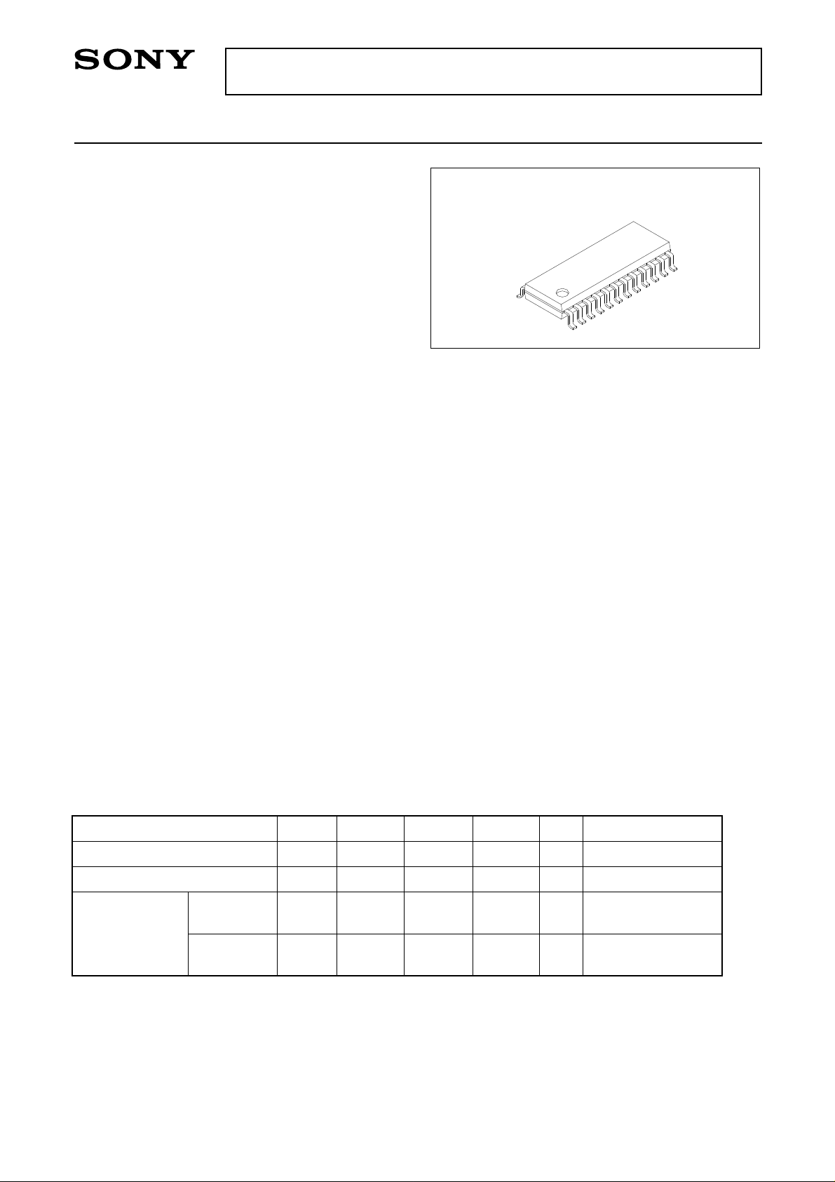
24 pin SOP (Plastic)
Structure
CMOS-CCD
Absolute Maximum Ratings (Ta = 25°C)
• Supply voltage VDD 6V
•Operating temperature Topr –10 to +60 °C
• Storage temperature Tstg –55 to +150 °C
• Allowable power dissipation PD 500 mW
Recommended Operating Conditions (Ta = 25°C)
Supply voltage VDD 5 ± 5% V
Recommended Clock Conditions (Ta = 25°C)
Item
Clock voltage Low
Clock voltage High
CXL1503M
Clock frequency
CXL1505M
Symbol
VL
VH
fCL
fCL
Min.
0
VDD – 1.0
Typ.
4.77
7.16
Max.
1.0
VDD
Unit
V
V
MHz
MHz
Remarks
NTSC: 910fH/3
CCIR: 908fH/3
NTSC: 455fH
CCIR: 454fH
Sony reserves the right to change products and specifications without prior notice. This information does not convey any license by
any implication or otherwise under any patents or other right. Application circuits shown, if any, are typical examples illustrating the
operation of the devices. Sony cannot assume responsibility for any problems arising out of the use of these circuits.
– 1 –
E89174A03-PS

CXL1503M/1505M
Block Diagram
ABCN
ABBL
DCAB
IN A
IN B
IN C
IN D
21
3
23
22
24
2
6
A. B
CENTER
A. B
BLACK
CLP
CLP
CLP
CLP
WAVE
FORM
7
CLP
Pin Description
Pin Configuration (Top View)
DD
N.C.
V
4
PG GEN.
PG GEN.
PG GEN.
PG GEN.
POTENTIAL
CONTROL
XDL1
19
P. D
5V
INPUT
SOURCE
5
IS
XDL2
18
TIMING GENERATOR
P. D
DL A
DL B
DL C
DL D
12
SS
DD
V
8
V
1
10
SS
V
16
CDS-OUTPUT
CIRCUIT
CDS-OUTPUT
CIRCUIT
CDS-OUTPUT
CIRCUIT
CDS-OUTPUT
CIRCUIT
14
GG
V
CDS
20
BIAS.
DD
SS
V
V
17
1
VSS
2
IN C
3
ABBL
4
DD
V
5
IS
6
15
OUT A
13
OUT B
OUT C
11
9
OUT D
IN D
CLP
V
OUT D
V
OUT C
N.C.
DD
GG
7
8
9
10
11
12
24
23
22
21
20
19
18
17
16
15
14
13
IN B
DCAB
IN A
ABCN
DD
V
XDL1
XDL2
SS
V
VSS
OUT A
CDS
OUT B
No.
1, 16, 17
2
3
4, 8, 20
5
6
7
9
10
11
12
13
14
15
18
19
Symbol
VSS
IN C
ABBL
VDD
IS
IN D
CLP
OUT D
VGG
OUT C
N.C.
OUT B
CDS
OUT A
XDL2
XDL1
I/O
GND
—
Signal input C channel
I
Autobias DC output for Y signal
O
5V power supply
—
Input source DC output
O
Signal input D channel
I
Clamp pulse input
I
Signal output D channel
O
Gate bias DC output
O
Signal output C channel
O
—
Signal output B channel
O
DC output for CDS
O
Signal output A channel
O
Clock pulse input 2
I
Clock pulse input 1
I
Description
—
Impedance (Ω)
> 100k (at no clamp)
2k to 20k
5k
> 100k (at no clamp)
> 100k
50 to 500
2k to 10k
50 to 500
50 to 500
500 to 5k
50 to 500
> 100k
> 100k
21
22
23
24
ABCN
IN A
DCAB
IN B
Autobias DC output for C signal
O
Signal input A channel
I
DC bias input for A and B channel
I
Signal input B channel
I
2k to 20k
> 100k (at no clamp)
> 100k
> 100k (at no clamp)
– 2 –

V
4.0
2.0
1.0
V
4.2
2.2
1.2
Unit
Max.
Typ.
CL = 4.77MHz (CXL1503M)
f
fCL = 7.16MHz (CXL1505M)
V
3.0
0.6
0.3
V
3.5
2.3
1.2
V
3.0
0.8
0.3
35
20
—
mA
40
30
—
dB
–0.5
–3.5
–4.5
dB
—
–0.8
–1.8
—
–0.4
–1.5
%
12
5
0
%
15
5
0
%
5
1
0
%
5
1
0
CXL1503M/1505M
%
3
1
0
DD = 5.0V, VSS = 0V)
Conditions Min.
(Ta = 25°C, V
E1
Bias condition
SW4 to 7
SW3
SW position
SW2
SW1
Test
Point
Output amplitude (mVp-p)
Output amplitude (SIN 1MHz, 100mVp-p)
Input amplitude (SIN 100kHz, 100mVp-p)
20 log
1
V
V2 – 0.2V
A, Bch → V1
C, Dch →
a
a
a
a
a
a
a
Output amplitude (SIN 100kHz, 100mVp-p)
(Note 1)
(Note 2)
(Note 3)
20 log
↓
a
(Note 3)
↓
a
(Note 4)
A, Bch → V1
C, Dch →
V2 – 0.2V
a ←→ b
a
a
a
a
a
a
b
b
a
a
a
a
a
a
a
a
a
b
V1
V2
V3
V4
V5
A1
a to d
b
b
V6
a to d
b
c
V6
a to d
b
b
V6
a to d
b
a
V6
ABCN
Symbol
ABBLISCDS
Item
Autobias center level
Electrical Characteristics
Autobias black level
GG
IDD
V
CXL1503M
1
∗
Input source level
CDS source level
Output circuit bias level
Supply
current
IG
CXL1505M
Insertion gain
– 3 –
fG
Lin.
CXL1503M
CXL1505M
∗1
Frequency
response
Linearity
∆G
∆LAB
∆LCD
Ach ←→ Bch
Cch ←→ Dch
Insertion gain difference
between channels
Linearity
difference
between
CRT
channels
Cross talk
Standerd values are different between CXL1503M and CXL1505M.
between channels
∗1
 Loading...