


CMOS-CCD 1H Delay Line for NTSC
Description
The CXL1504M is a delay line used in conjunction
with an external low-pass filter. Through negative
phase input and positive phase output 1H delay time
is obtained for NTSC signals.
Features
• Single 5V power supply
• 14.3MHz driver
• Low power consumption at 160mW (Typ.)
• Built-in peripheral circuits
• Completely adjustment free
Functions
• 905.5-bit CCD register
• Clock driver
• Autobias circuit
• Input clamp circuit
• Sample and hold circuit
Structure
CMOS-CCD
Absolute Maximum Ratings (Ta = 25°C)
• Supply voltage VDD 6V
•Operating temperature Topr –10 to +60 °C
• Storage temperature Tstg –55 to +150 °C
• Allowable power dissipation PD 500 mW
Operating Voltage Range (Ta = 25°C)
Supply voltage VDD 5 ±5% V
Recommended Clock Conditions (Ta = 25°C)
• Input clock amplitude VCLK 0.3 to 1.0 Vp-p (0.5Vp-p typ.)
• Clock frequency fCLK 14.318182 MHz
• Input clock waveform sine wave
Input Signal Amplitude
VSIG 560 mVp-p (Max.)
– 1 –
E71217A78-PS
Sony reserves the right to change products and specifications without prior notice. This information does not convey any license by
any implication or otherwise under any patents or other right. Application circuits shown, if any, are typical examples illustrating the
operation of the devices. Sony cannot assume responsibility for any problems arising out of the use of these circuits.
CXL1504M
20 pin SOP (Plastic)

– 2 –
CXL1504M
Block Diagram and Pin Configuration (Top View)
2
3
6
7
8
9
10
11
12
13
14
15
17
18
19
20
IS
AB
NC
IN
V
DD
V
SS
V
GG
A
OUT
V
SS
V
GG
B
SUB
NC
NC
V
DD
CLK
V
SS
NC
V
DD
NC
V
SS
Bias circuit
(B)
Bias circuit
(A)
4
5
CCD (905.5bit)
Clock
driver
Output circuit,
S/H circuit
Pulse generation
circuit
1
16
φ1 φ2
φS/H
Autobias
circuit
Pin Description
Pin No. Symbol I/O Description Impedance [Ω]
1
2
3
4
5
6
7
8
9
10
11
12
13
14
15
16
17
18
19
20
IS
AB
NC
IN
VDD
VSS
VGGA
OUT
VSS
VGGB
VSS
NC
VDD
NC
VSS
CLK
VDD
NC
NC
SUB
O
O
—
I
—
—
O
O
—
O
—
—
—
—
—
I
—
—
—
—
CCD bias DC output
Autobias DC output
Signal input (Negative phase signal)
5V power supply (For clock driver)
GND
Gate bias (A) DC output
Signal output (Positive phase signal)
GND
Gate bias (B) DC output
GND
5V power supply (For analog system)
GND
Clock input
5V power supply (For digital system)
GND
600 to 2k
2k to 20k
> 100k (at no clamp)
2k to 10k
40 to 500
2k to 10k
4k to 50k
– 3 –
CXL1504M
Electrical Characteristics
(Ta = 25°C, VDD = 5V, fCLK = 14.318182MHz, VCLK = 500mVp-p, sine wave)
See the Electrical Characteristics Test Circuits.
Item Symbol Test conditions
SW conditions
Min. Typ. Max. Unit Note
(Note 1)
Bias conditions
VBIAS1 [V]
1
2 3 4
—
b
b
c
c
a
d
a
a
b
a
a
b
a
a
a
a
a
a
b
a
a
a
b
c
d
d
—
e
—
200kHz,
500mVp-p,
sine wave
200kHz ←→3.58MHz,
150mVp-p,
sine wave
5-staircase wave
(See Note 5)
5-staircase wave
(See Note 5)
No signal input
50% white video
signal
(See Note 7)
IDD
GL
fr
DG
DP
CP
S/N
Supply
current
Low
frequency
gain
Frequency
response
Differential
gain
Differential
phase
S/H pulse
coupling
S/N ratio
←→
Notes
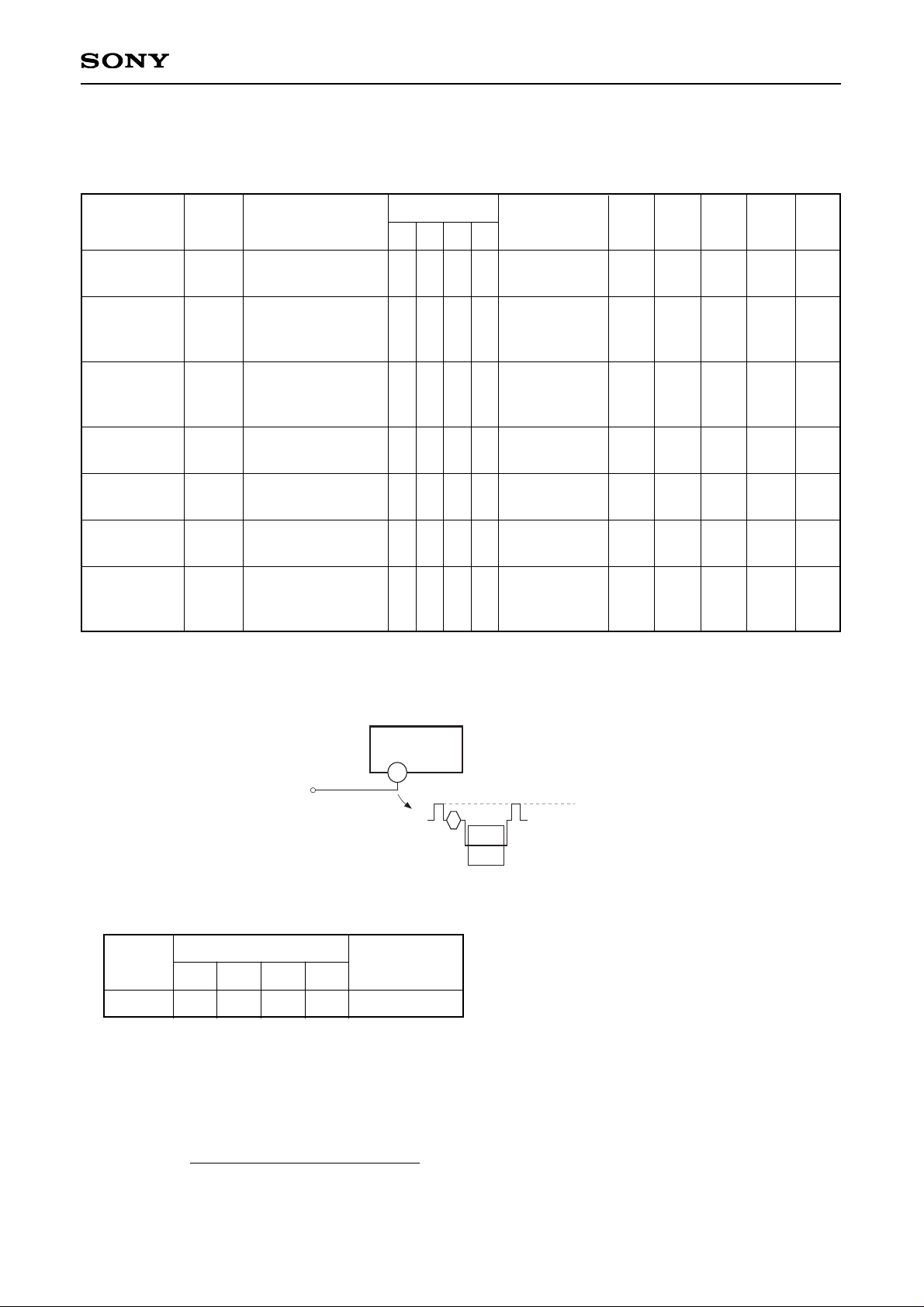
1) VIN is defined as follows.
VIN is the input signal clamp level, it clamps the video signal sync tip level.
CXL1504
Input
(IN)
Clamp level VIN
4
Negative phase
signal input
VIN is the pin voltage for Pin 4 at no-input signal. Testing is executed with a voltmeter under the follwing SW
conditions.
As VIN varies with each IC, they are all subject to testing.
2) IDD is the IC supply current value during clock and signal input.
3) GL is the OUT pin output gain when a 500mVp-p, 200kHz sine wave is input to IN pin.
GL = 20 log [dB]
SW conditions
Item
VIN
Test point
V1
1
—
2
b
3
a
4
—
—
—
VIN – 0.2
—
—
VIN
—
mA
dB
dB
%
degree
mVp-p
dB
42
–1.0
0
7
7
350
—
32
–3.0
–1.3
3
3
200
56
20
–5.0
–2.5
0
0
—
54
2
3
4
5
5
6
7
OUT pin output voltage [mVp-p]
500 [mVp-p]
 Loading...