

Sony CXL1008P, CXL1008M Datasheet

CXL1008M/P
CMOS-CCD Signal Processor for Skew Compensation
Description
CXL1008M/P are CMOS-CCD signal processors
developed for the variable-speed video signal processor
for home-use 8mm VCRs.
Features
• Low power consumption 105mW (Typ.)
• Built-in peripheral circuit
• Adjustment is necessary for one part.
Structure
CMOS-CCD
Functions
• 1/2H 359-bit, direct 20-bit CCD register
• Clock driver
• Timing oscillation circuit
• Automatic bias circuit
• Sync tip clamp circuit
• Dummy VD insert circuit
• Sample/hold circuit
CXL1008M
28 pin SOP (Plastic)
CXL1008P
28 pin DIP (Plastic)
Absolute Maximum Ratings (Ta = 25°C)
• Supply voltage VDD 11 V
VCL 6V
•Operating temperature Topr –10 to +60 °C
• Storage temperature Tstg –55 to +150 °C
• Allowable power dissipaiton
PD CXL1008M 500 mW
CXL1008P 1000 mW
Recommended Operating Conditions
Supply voltage VDD 9V ± 5 %
VCL 5V ± 5 %
Recommended Clock Conditions
• Clock input amplitude VCLK 0.15 to 1.0 (0.3 Typ.) Vp-p
• Clock frequency fCLK 10.738635 MHz
Sony reserves the right to change products and specifications without prior notice. This information does not convey any license by
any implication or otherwise under any patents or other right. Application circuits shown, if any, are typical examples illustrating the
operation of the devices. Sony cannot assume responsibility for any problems arising out of the use of these circuits.
– 1 –
E60248-PS
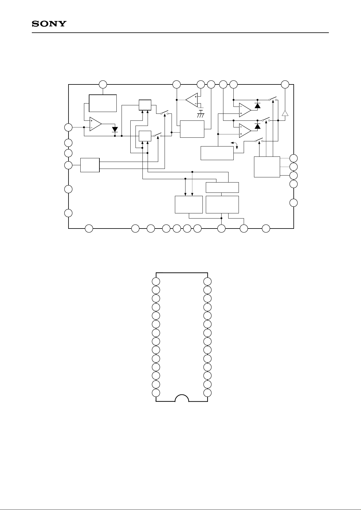
Block Diagram
13
AUTO
FEED OUT
24
FEED IN
25
CCD OUT
23
21
SIG DELAY
SIG IN2
12
CXL1008M/P
SIG OUT
19
AUTOBIAS
CIRCUIT
T10
T9
T1
T2
11
28
27
26
SKEW
2
3
SIG IN1
SKEW IN
4
T3
Pin Configuration (Top View)
1/2H
OUTPUT
D
CIRCUIT
50mV
50mV
REFERENCE
OUTPUT
φ1
CONTROL
φ2
DRIVER
DUTY
CONTROL
6
5
T4
T5
18
1
SS
V
SS
V
14
20
CL
V
TIMING
GENERATOR
DD
V
7
CLK IN
22
REC/PB
8
T6
10
17
16
15
9
MUTE IN
JOG IN
EXT VD
T8
T7
T8
EXT VD
JOG IN
V
SIG OUT
DD
V
SIG DELAY
REC/PB
CCD OUT
FEED OUT
FEED IN
SKEW IN
T9
T10
SS
15
16
17
18
19
20
23
21
22
24
25
26
27
28
14
13
12
11
10
9
8
7
6
5
4
3
2
1
VCL
AUTO
SIG IN2
SIG IN1
MUTE IN
T7
T6
CLK IN
T5
T4
T3
T2
T1
SS
V
– 2 –

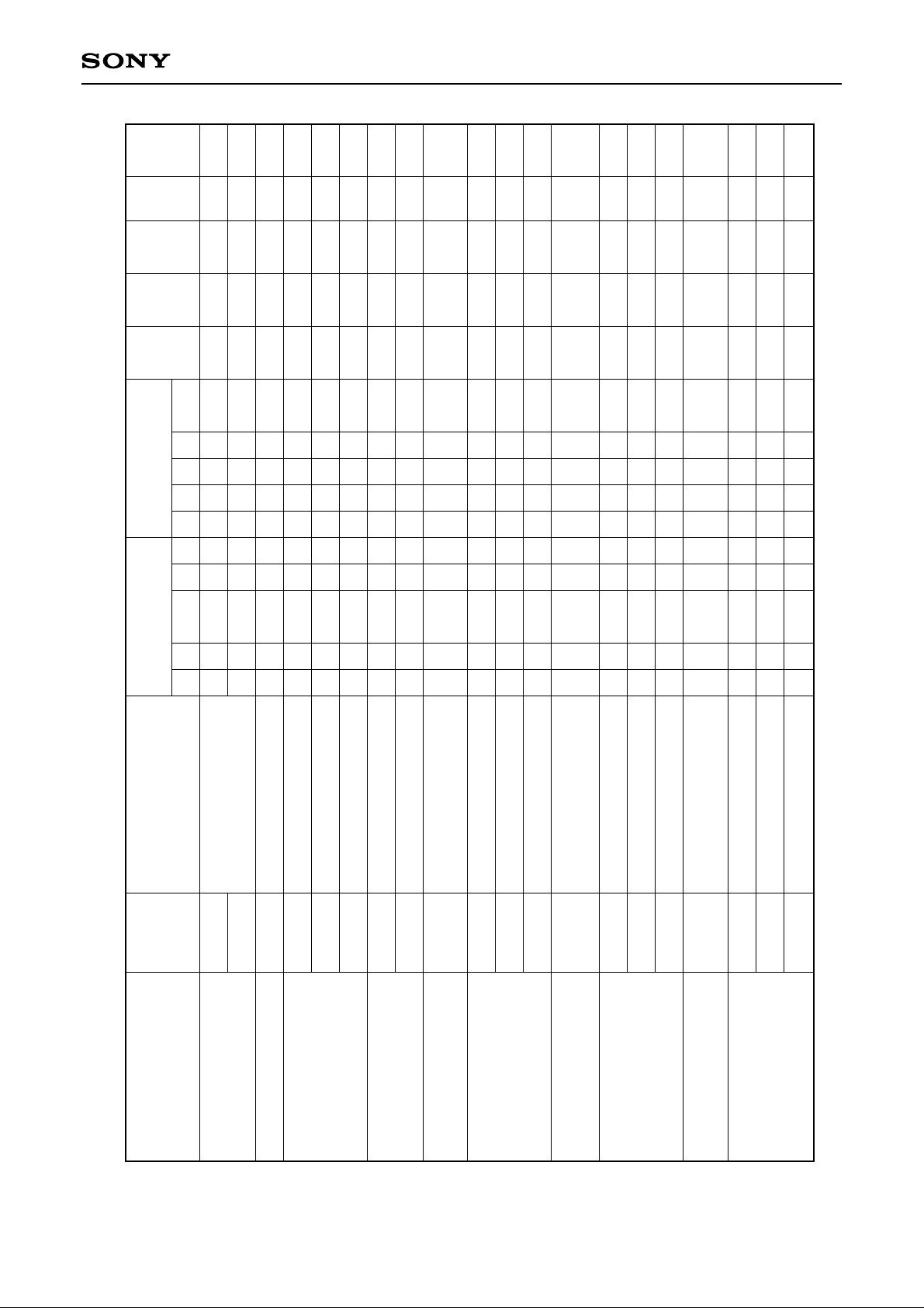
Pin Description
CXL1008M/P
Pin
No.
1
7
10
11
12
13
14
16
17
18
Symbol I/O
VSS
CLK IN
MUTE IN
SIG IN1
SIG IN2
AUTO
VCL
EXT VD
JOG IN
VSS
I
0.3Vp-p
5V when
I
muting,
normally 0V
1.1Vp-p or
I
less
2.2Vp-p or
I
less
O
+5V
5V when VD
I
is inserted
JOG mode
I
PB/REC
mode 0V
Supply
voltage
Description
GND
Input the sine wave of 3fsc (10.738635MHz)
The video signal mute is generated at High level.
See the Logic Table of Signal Output Selection
State (Table 1).
Signal input pin of CCD DL.
Input composite video signal.
Signal input pin of the through side.
Input composite video signal.
The DC level of automatic bias is output.
Power supply 1
Use this pin when VD is inserted to the video signal
with the extrenal dummy VD signal input.
JOG/NORMAL PB selection pin.
5V
See the Logic Table of Signal Output Selection
State (Table 1).
GND
Impedance
(Ω)
> 50k
> 100k
> 100k
> 100k
10k
> 100k
> 100k
19
20
21
22
23
24
25
SIG OUT
VDD
SIG DELAY
REC/PB
CCD OUT
FEED OUT
FEED IN
O
+9V
I
5V when PB
I
0V when REC
O
O
I
Final output
Power supply 2
After the output from Pin 23 CCD OUT passes through
LPF, input it to the same pin and insert clamp and VD.
Operate the clock at High when PB.
Stop the clock at Low when REC.
Direct output from CCD DL
Feedback DC output
Smoothing capacitor connection pin of the bias
commutation loop on the output circuit
0.6 to 1.5k
> 100k
> 100k
0.6 to 1.5k
10k
> 100k
Select Direct DL and 1/2H DL signals when High
26
SKEW IN
I
and Low, respectively.
See the Logic Table of CCD DL Mode Selection
> 100k
(Table 2).
Note) T1 through T10 test pins must be connected as shown in the application circuit because of the IC
internal circuit.
Notes on Handling
Countermeasures for electrostatics are necessary because some pins have low electrostatic strength
(particularly Pin 26: SKEW IN).
– 3 –
Unit Note
Max.
Min. Typ.
1
mA
12
7
1
mA
10
8
V
1.0
0.3
0.15
2
V
6.0
5.0
4.0
2
V
4.4
4.2
4.0
2
V
4.4
4.2
4.0
3
V
2.4
2.0
1.7
3
V
2.5
2.0
1.5
4
mV
55
0
–55
5
dB
3.0
0
–3.0
5
dB
0
–0.8
–1.2
5
dB
0
–0.8
–1.2
6
%
1.3
0
–1.3
7
dB
0
–2
–3
8
dB
—
0
–0.5
8
dB
—
0
–0.5
9
dB
0.2
0
–0.2
CXL1008M/P
10
10
%
%
4
10
3
2
0
0
10
%
4
2
0
H
H
∗1, ∗2
P2 P3 P4 P5
Control Pin Conditions
DD = 9.0V, VCL = 5.0V, fCLK = 10.7MHz, VCLK = 0.3Vp-p sine wave)
a
a
2 3 4 5 P1
a
a
Switch Conditions
c
1
c
H ←→ L
H
H
e
e
a
a
c
b
H
e
e
a
a
c
a
H
H
L
L
L
a
a
e
e
a
a
c
b
L
L
L
a
a
a
b
f
a
b
b
c
b
H ←→ L
H
H
H
L
L
a
a
b
a
f
a
b
b
c
a
L
L
L
b
b
a
b
b ←→ c
b ←→ d
b
b
c
b
H ←→ L
H
H
H
L
L
b
b
b
a
b ←→ c
b ←→ d
b
b
c
a
L
H
L
L
L
L
c
c
c
a
b
b
g
g
g
b
b
b
c
b
a
PB, JOG
Symbol Test Conditions
DD
I
ICL
Items
Electrical Characteristics
(See the Electrical Characteristics Test Circuit) (Ta = 25°C, V
Power current
CLK
Vdi1
Vdi2
Vdi3
Clock input level
Signal input pin voltage
Direct ←→ 1/2H
Vdo1
Vdo2
∆Dab
IGCCD
IGIn2
Signal output pin voltage
CCD signal output
voltage difference
Signal insert gain
– 4 –
Direct ←→ 1/2H
3.58MHz/100kHz
10MHz/100kHz
IGDL
∆Gab
fCCD
fIn2
CCD output signal gain
difference
Frequency characteristics
10MHz/100kHz
Direct ←→ 1/2H at 3.58MHz
1.1Vp-p input
2.2Vp-p input
2.2Vp-p input
fDL
∆fab
DGCCD
DGIn2
DGDL
Frequency characteristics
difference
Differential gain
 Loading...