

SONY CXK77B3610GB Technical data
查询CXK77B3610GB供应商
CXK77B3610GB
High Speed Bi-CMOS Synchronous Static RAM
Description
The CXK77B3610GB-6/7 is a high speed 1M bit
Bi-CMOS synchronous statis RAM organized as
32768 words by 36 bits. This SRAM integrates input
registers, high speed SRAM and write buffer onto a
single monolithic IC and features the delayed write
system to reduce the dead cycles.
Features
• Fast cycle time (Cycle) (Frequency)
CXK77B3610GB-6 6ns 166MHz
CXK77B3610GB-7 7ns 142MHz
• Inputs and outputs are LVTTL/LVCMOS compatible
• Single 3.3V power supply: 3.3V ± 0.15V
• Byte-write possible
• OE asynchronization
• JTAG test circuit
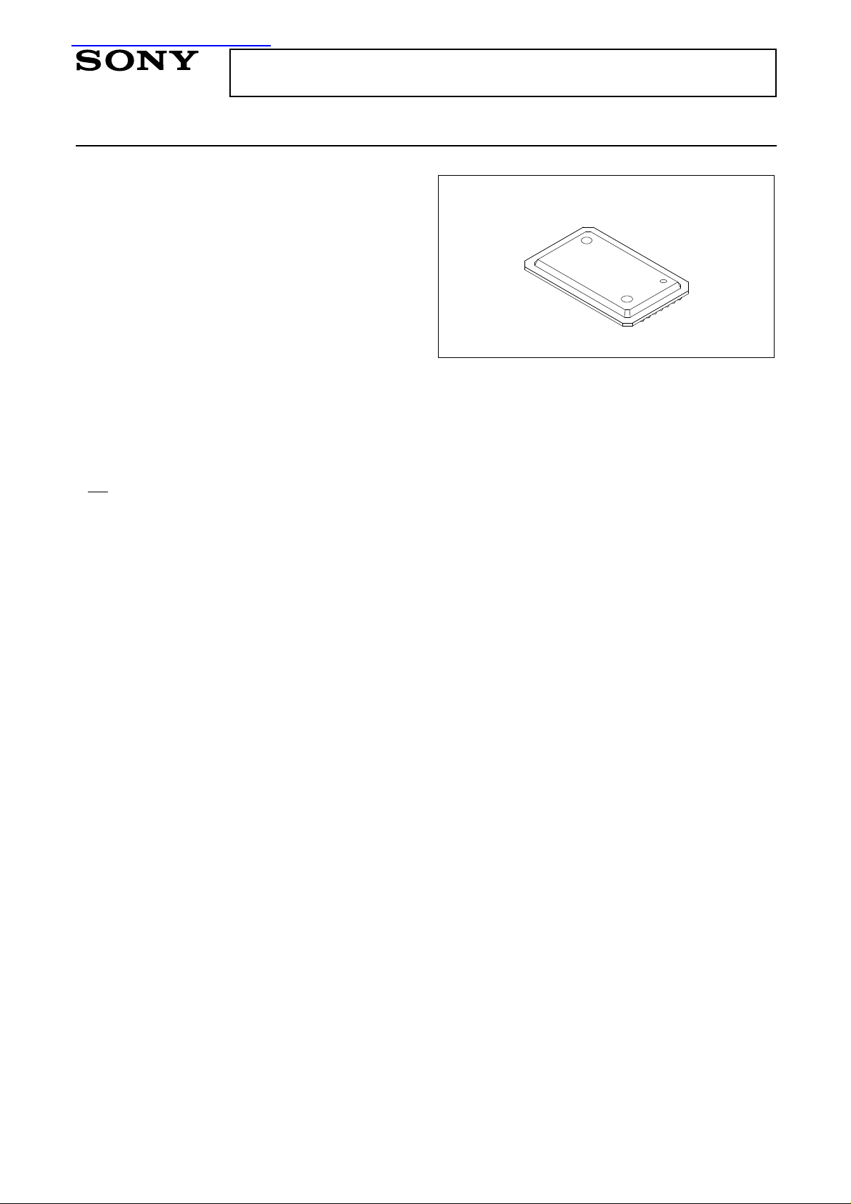
• Package 119TBGA
• 3 kinds of synchronous operation mode
Register-Register mode (R-R mode)
Register-Flow Thru mode (R-F mode)
Register-Latch mode (R-L mode)
-6/7
Preliminary
119 pin BGA (Plastic)
Function
32768 word × 36bit High Speed Bi-CMOS Synchronous SRAM
Structure
Silicon gate Bi-CMOS IC
Sony reserves the right to change products and specifications without prior notice. This information does not convey any license by
any implication or otherwise under any patents or other right. Application circuits shown, if any, are typical examples illustrating the
operation of the devices. Sony cannot assume responsibility for any problems arising out of the use of these circuits.
– 1 –
PE95128-PS
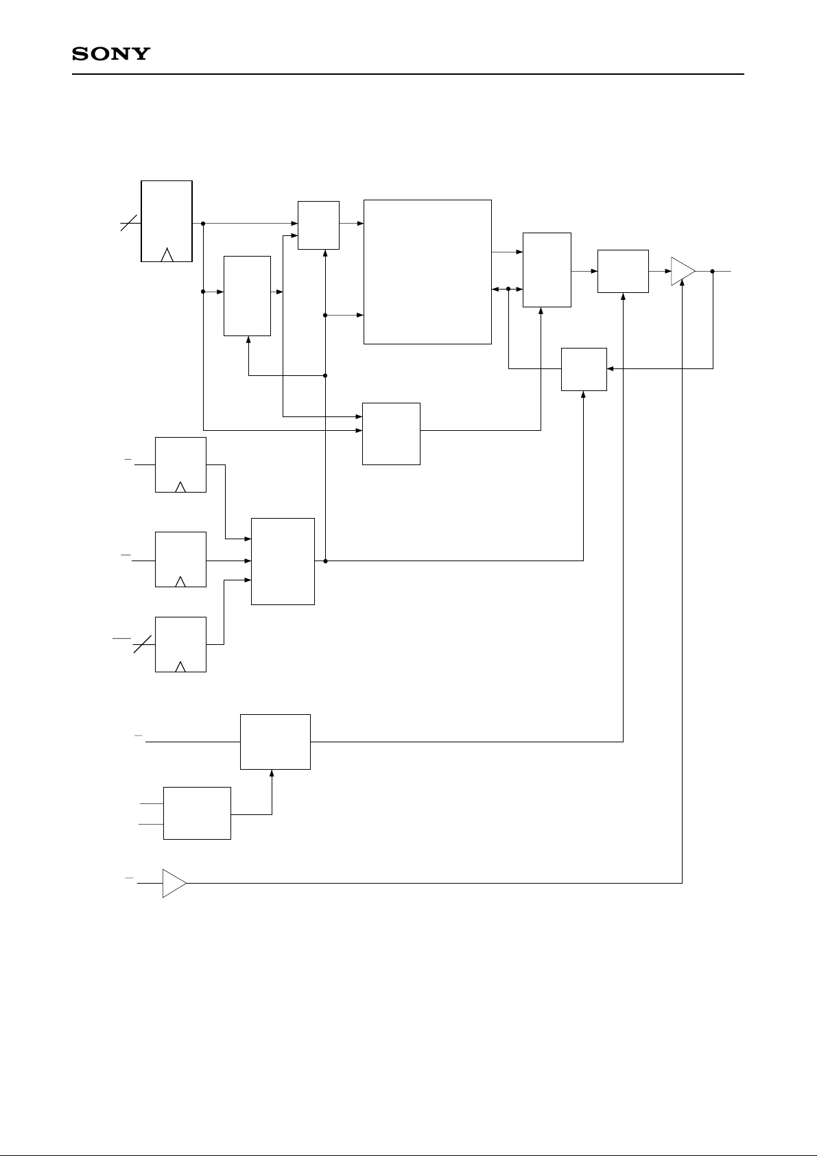
Block Diagram
15
A0 to 14
Input
Reg.
Write
Store
Reg.
2:1
Mux
Add.
Write
pulse
Read
Comp.
32K × 36
Dout
Din
2:1
Mux
Reg.
Output
latch
CXK77B3610GB
DQ
BW
S
W
a to d
K/K
M1
M2
Reg.
Salf
Reg.
4
Reg.
Mode
Control
Time
Write
Logic
Output
Clock
G
– 2 –
Pin Configuration (Top View)
1234567
A
B
C
D
E
F
G
H
J
K
L
M
VDDQ
NC
NC
DQc
DQc
VDDQ
DQc
DQc
VDDQ
DQd
DQd
VDDQ
A
NC
A
DQc
DQc
DQc
DQc
DQc
VDD
DQd
DQd
DQd
A
NC
A
VSS
VSS
VSS
BWc
VSS
NC
VSS
BWd
VSS
NC
NC
VDD
NC
S
G
NC
NC
VDD
K
K
W
A
NC
A
VSS
VSS
VSS
BWb
VSS
NC
VSS
BWa
VSS
A
NC
A
DQb
DQb
DQb
DQb
DQb
VDD
DQa
DQa
DQa
CXK77B3610GB
VDDQ
NC
NC
DQb
DQb
VDDQ
DQb
DQb
VDDQ
DQa
DQa
VDDQ
N
DQd
P
DQd
R
NC
T
NC
U
VDDQ
DQd
DQd
A
NC
TME
VSS
VSS
M1
A
TDI
A
A
VDD
A
TCK
VSS
VSS
M2
A
TDO
DQa
DQa
A
NC
NC
DQa
DQa
NC
ZZ
VDDQ
Pin Description
Symbol Description Symbol Description Symbol Description
A
DQx
K
K
W
Address Input
Data I/O in byte
a to d
Positive Clock
Negative Clock
Write Enable
G
ZZ
TCK
TMS
TDI
Asyn Output Enable
Sleep Mode Select
JTAG Clock
JTAG Mode Select
JTAG Data In
VDDQ
VSS
M1, M2
NC
Output power supply
Ground
Mode Select
No Connect
BWx
S
Byte Write Enable
(a to d)
Chip Select
TDO
VDD
JTAG Data Out
+3.3V power supply
– 3 –
Absolute Maximum Ratings (Ta = 25°C, GND = 0V)
CXK77B3610GB
Item
Supply voltage
Input voltage
Output voltage
Allowable power dissipation
operating temperature
Strorage temperature
Soldering temperature · time
Symbol
VCC
VIN
VO
PD
Topr
Tstg
Tsolder
Rating
–0.5 to +4.6
–0.5 to VCC +0.5 (4.6V max.)
–0.5 to VCC +0.5 (4.6V max.)
0 to 70
–55 to +150
235 · 10
Truth Table
ZZ S (tn) W (tn) BWx (tn) G Mode
H
L
L
L
L
X
H
L
L
L
X
X
H
H
L
X
X
X
X
L
X
X
H
L
X
Sleep mode, Power down
Deselect
Read
Read
Write all bytes (bits 0 to 35)
TBD
Unit
V
V
V
W
°C
°C
°C · sec
DQ0 to 35
(tn)
Hi-Z
X
Hi-Z
X
X
DQ0 to 35
(tn+1)
Hi-Z
Hi-Z
Hi-Z
Q (tn)
D (tn)
VDD
Current
ISB
ICC
ICC
ICC
ICC
L
L
L
L
L
L
X
H
X
X
Write bytes with BWx = L
Aborted Write
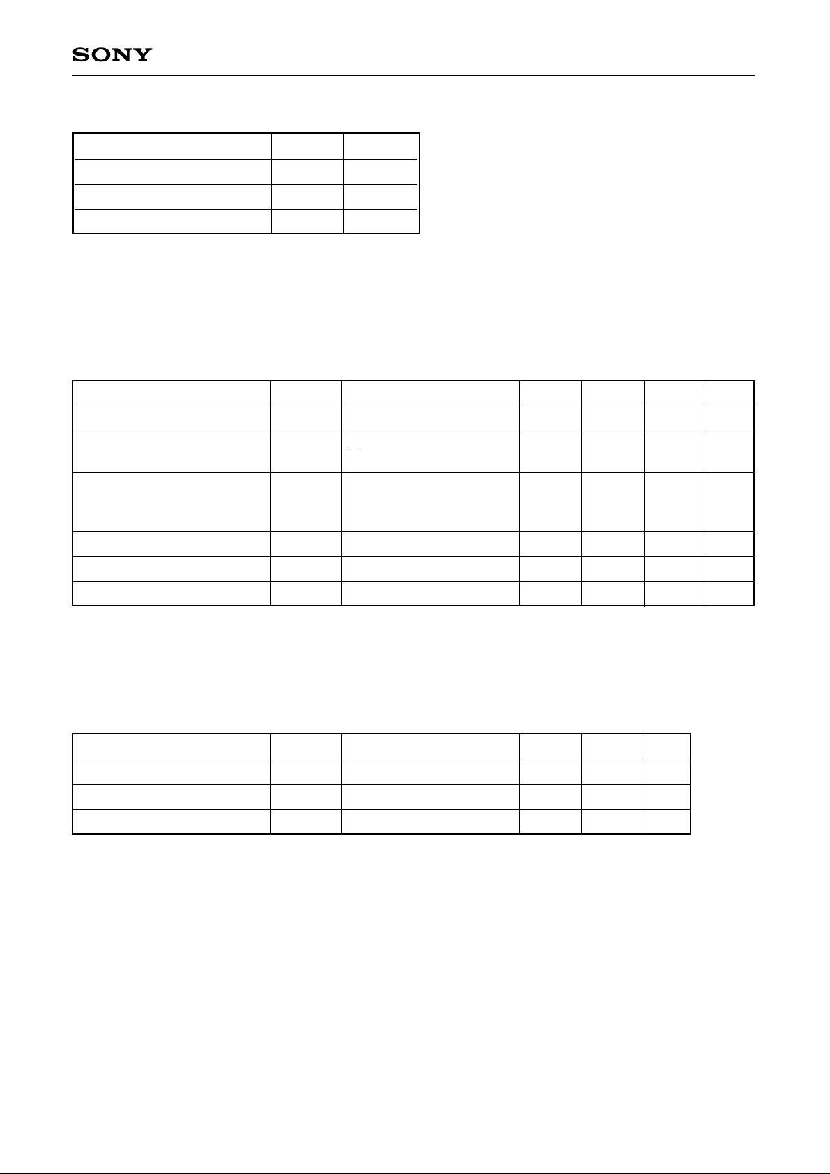
DC Recommended Operating Conditions (Ta = 25°C, GND = 0V)
Item
Supply voltage
Output supply voltage
Input high voltage
Input low voltage
Differential clock input signal
Differential clock input
common mode
Symbol
VDD
VDDQ
VIH
VIL
∆VK
VK, COM
Min.
3.15
3.15
2.0
–0.3
0.4
1.2
Typ.
3.3
3.3
—
—
0.8
2.0
Max.
3.45
3.45
VDD +0.3
0.8
—
2.2
Unit
V
V
V
V
V
V
X
X
D (tn)
X
ICC
ICC
– 4 –
Mode Select Truth Table
CXK77B3610GB
Item
Register-Resister mode
Register-Flow Thru mode
Register-Latch mode
M1
L
L
H
M2
H
L
L
Electrical Characteristics
• DC and operating characteristics (VCC = 3.3V ± 10%, GND = 0V, Ta = 0 to 70°C)
∗
Item
Input leakage current
Output leakage current
Operating power supply
current
Standby current
Symbol
ILI
ILO
ICC
ISB
Test conditions
VIN = GND to VCC
VO = GND to VCC
G = VIH
Cycle = min.
Duty = 100%
IOUT = 0mA
ZZ ≥ VIH
Min.
–1
–10
—
Typ.
—
—
—
Max.
1
10
TBD
20
Unit
µA
µA
mA
mA
Output high voltage
Output low voltage
∗
VCC = 3.3V, Ta = 25°C
VOH
VOL
IOH = –2.0mA
IOL = 2.0mA
2.4
—
—
—
—
0.4
• I/O capacitance (Ta = 25°C, f = 1MHz)
Item
Input capacitance
Clock input capacitance
Output capacitance
Symbol
CIN
CCLK
COUT
Test conditions
VIN = 0V
VIN = 0V
VOUT = 0V
Min.
—
—
—
Max.
5
8
8
Unit
pF
pF
pF
Note) These parameters are sampled and are not 100% tested.
V
V
– 5 –
 Loading...