

Sony CXK77B1810AGB-6, CXK77B1810AGB-5 Datasheet
CXK77B1810AGB
For the availability of this product, please contact the sales office.
-5/6
High Speed Bi-CMOS Synchronous Static RAM
Description
The CXK77B1810AGB-5/6 is a high speed 1M bit
Bi-CMOS synchronous static RAM organized as
65536 words by 18 bits. This SRAM integrates input
registers, high speed SRAM and write buffer onto a
single monolithic IC and features the delayed write
system to reduce the dead cycles.
Features
• Fast cycle time (Cycle) (Frequency)
CXK77B1810AGB-5 5ns 200MHz
-6 6ns 167MHz
• Inputs and outputs are GTL/HSTL compatible
• Controlled Impedance Driver
• Single 3.3V power supply: 3.3V±0.15V
• Byte-write possible
• OE asynchronization
• JTAG test circuit
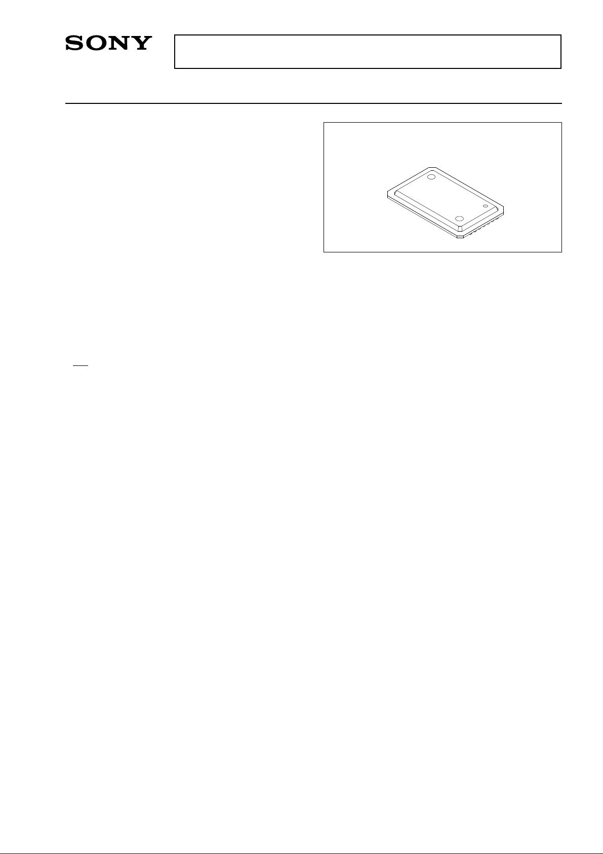
• Package 119TBGA
• 4 kinds of synchronous operation mode
Register-Register mode (R-R mode)
Register-Flow Thru mode (R-F mode)
Register-Latch mode (R-L mode)
Dual clock mode (D-C mode)
Preliminary
119 pin BGA (Plastic)
Function
65536 word x 18bit High Speed Bi-CMOS Synchronous SRAM
Structure
Silicon gate Bi-CMOS IC
Sony reserves the right to change products and specifications without prior notice. This information does not convey any license by
any implication or otherwise under any patents or other right. Application circuits shown, if any, are typical examples illustrating the
operation of the devices. Sony cannot assume responsibility for any problems arising out of the use of these circuits.
– 1 –
PE96811
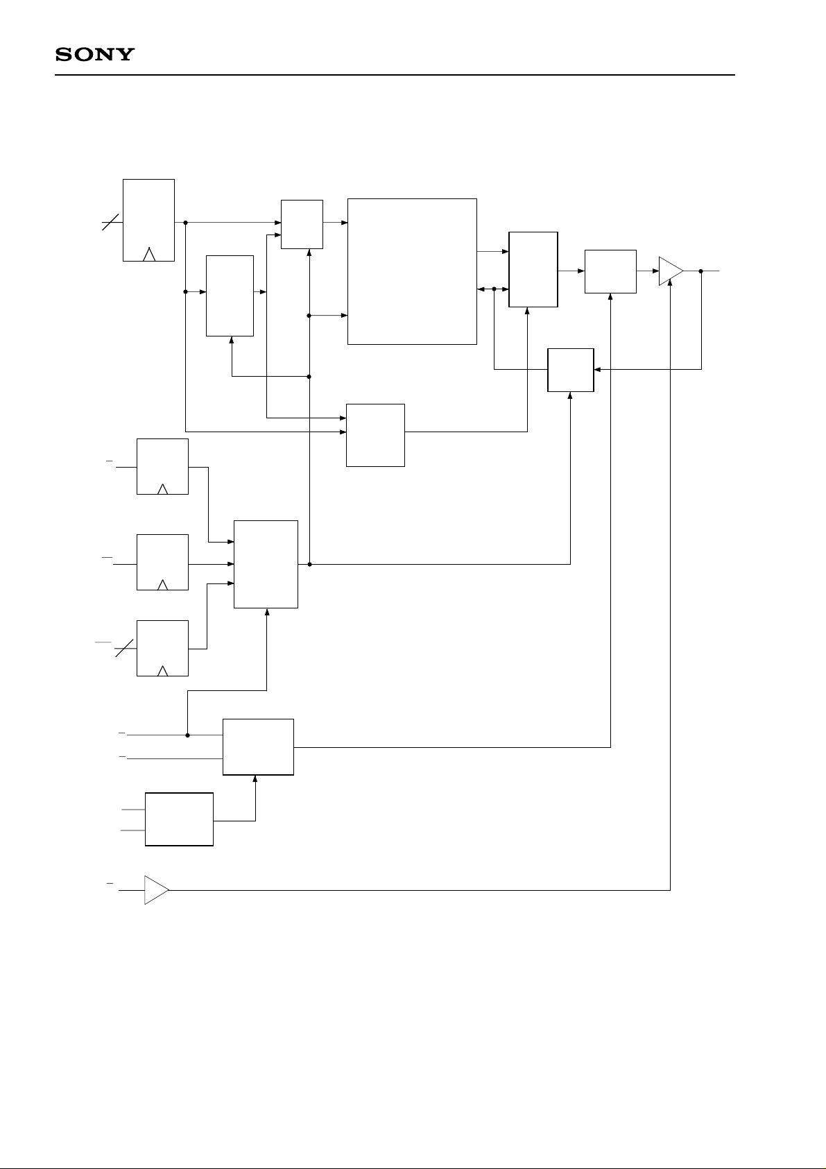
Block Diagram
16
A0 to 15
Input
Reg.
Write
Store
Reg.
2:1
Mux
Add.
Write
pulse
Read
Comp.
64K × 18
Dout
Din
2:1
Mux
Reg.
Output
latch
CXK77B1810AGB
DQ
BW
S
W
a to b
K/K
C/C
M1
M2
Reg.
Self
Reg.
2
Reg.
Mode
Control
Time
Write
Logic
Output
Clock
G
– 2 –
 Loading...