

Sony CXK581000AP-70LL, CXK581000AP-55SL, CXK581000AP-55LL, CXK581000AP-10SL, CXK581000AP-10LL Datasheet
...
CXK581000ATM/AYM/AM/AP
For the availability of this product, please contact the sales office.
131072-word × 8-bit High Speed CMOS Static RAM
Description
The CXK581000ATM/AYM/AM/AP is a high speed
CMOS static RAM organized as 131072-words by
8 bits.
A polysilicon TFT cell technology realized extremely low
stand- by current and higher data retention stability.
Special feature are low power consumption, high
speed and broad package line-up.
The CXK581000ATM/AYM/AM/AP ia a suitable
RAM for portable equipment with battery back up.
Features
• Fast access time:
CXK581000ATM/AYM/AM/AP (Access time)
-55LL/55SL 55ns (Max.)
-70LL/70SL 70ns (Max.)
-10LL/10SL 100ns (Max.)
• Low standby current:
CXK581000ATM/AYM/AM/AP
-55LL/70LL/10LL 20µA (Max.)
-55SL/70SL/10SL 12µA (Max.)
• Low data retention current
CXK581000ATM/AYM/AM/AP
-55LL/70LL/10LL 12µA (Max.)
-55SL/70SL/10SL 4µA (Max.)
• Single +5V supply: +5V ±10%
• Low voltage data retention: 2.0V (Min.)
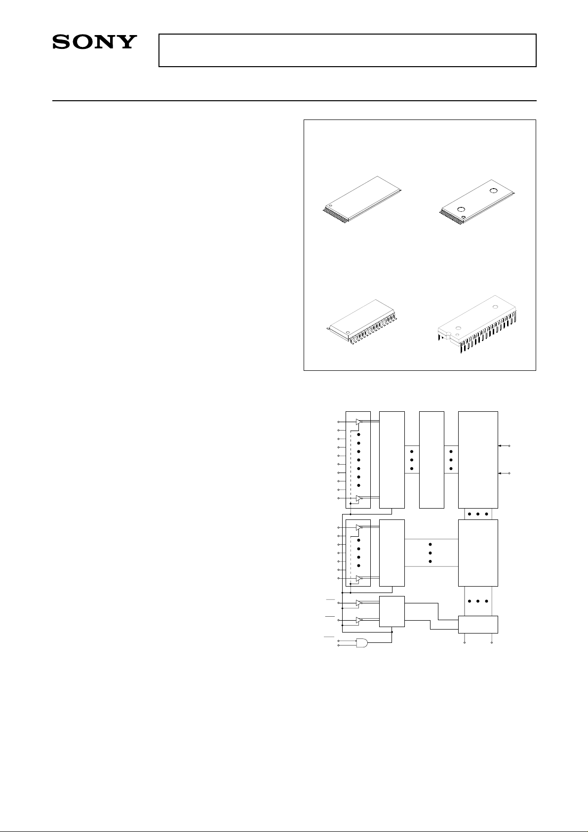
• Broad package line-up
• CXK581000ATM/AYM
8mm × 20mm 32 pin TSOP package
• CXK581000AM 525mil 32 pin SOP package
• CXK581000AP 600mil 32 pin DIP package
CXK581000ATM
32 pin TSOP (Plastic)
CXK581000AM
32 pin SOP (Plastic)
Block Diagram
A10
A11
A9
A8
A13
A15
A16
A14
A12
A7
A6
A5
A4
A3
A2
A1
A0
Buffer
Buffer
-55LL/70LL/10LL
-55SL/70SL/10SL
CXK581000AYM
32 pin TSOP (Plastic)
CXK581000AP
32 pin DIP (Plastic)
Row
Decoder
Memory
Matrix
1024 × 1024
I/O Gate
Column
Decoder
VCC
GND
Functions
131072-word × 8-bit static RAM
OE
WE
CE1
CE2
Buffer
I/O Buffer
I/O 1 I/O 8
Structure
Silicon gate CMOS IC
Sony reserves the right to change products and specifications without prior notice. This information does not convey any license by
any implication or otherwise under any patents or other right. Application circuits shown, if any, are typical examples illustrating the
operation of the devices. Sony cannot assume responsibility for any problems arising out of the use of these circuits.
– 1 –
E92756D53-PP
CXK581000ATM/AYM/AM/AP
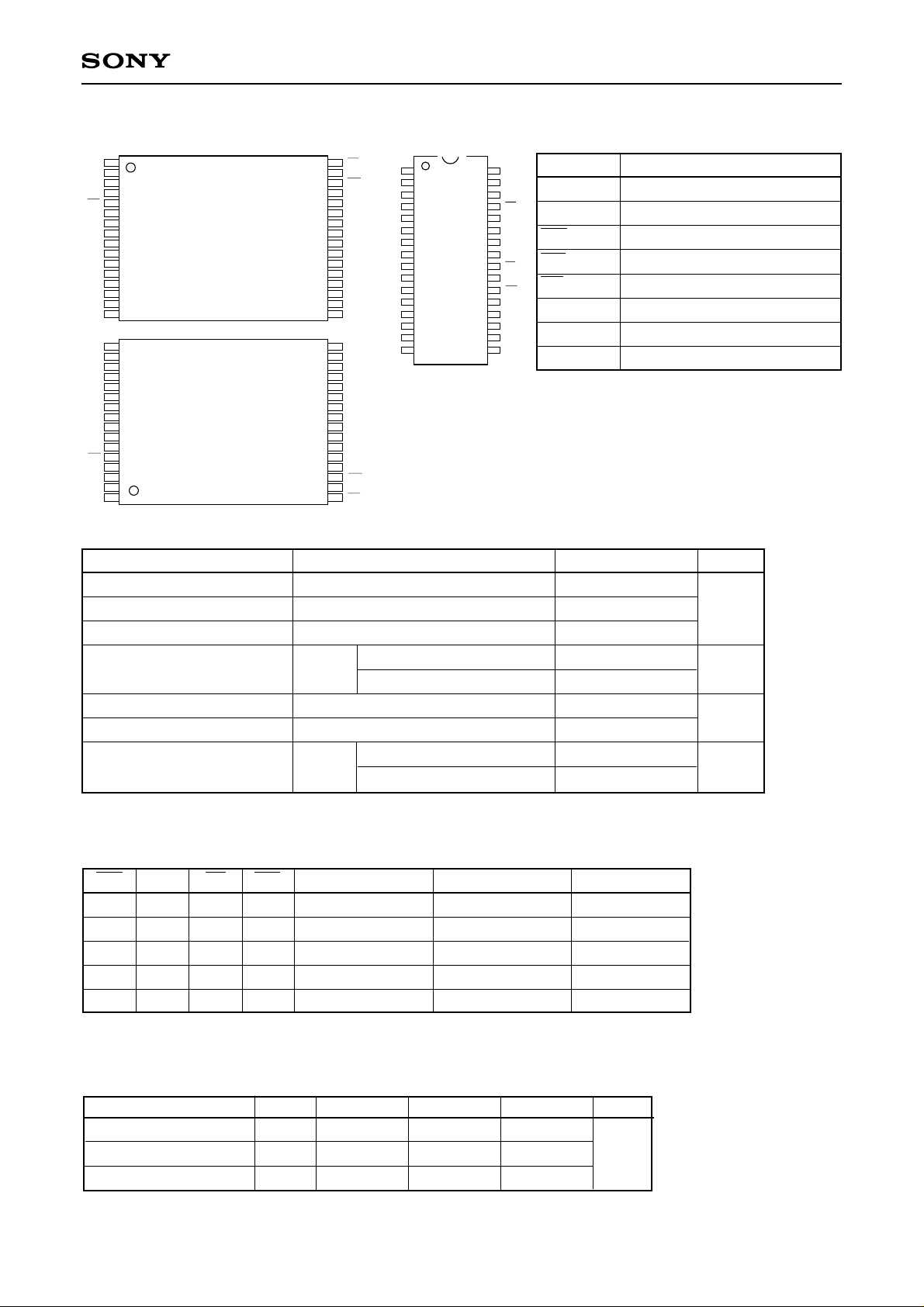
Pin Configuration (Top View)
1
A11
2
A9
3
A8
4
A13
5
WE
6
CE2
7
A15
8
VCC
A16
A14
A12
A12
A14
A16
V
A15
CE2
WE
A13
A11
9
NC
10
11
12
13
A7
14
A6
15
A5
16
A4
16
A4
15
A5
14
A6
13
A7
12
11
10
9
NC
8
CC
7
6
5
4
3
A8
2
A9
1
CXK581000ATM
(Standard Pinout)
CXK581000AYM
(Mirror Image Pinout)
OE
32
31
A10
CE1
30
29
I/O8
I/O7
28
27
I/O6
I/O5
26
25
I/O4
GND
24
23
I/O3
I/O2
22
21
I/O1
A0
20
19
A1
A2
18
17
A3
A3
17
A2
18
A1
19
A0
20
I/O1
21
I/O2
22
I/O3
23
GND
24
I/O4
25
I/O5
26
I/O6
27
I/O7
28
I/O8
29
CE1
30
A10
31
OE
32
1
NC
2
A16
3
A14
4
A12
5
A7
6
A6
7
A5
8
A4
9
A3
10
A2
11
A1
12
A0
13
I/O1
14
I/O2
15
I/O3
16
GND
CXK581000AM
CXK581000AP
Pin Description
32
VCC
31
A15
CE2
WE
A13
A8
A9
A11
OE
A10
CE1
I/O8
I/O7
I/O6
I/O5
I/O4
A0 to A16
I/O1 to I/O8
CE1, CE2
WE
OE
Vcc
GND
NC
30
29
28
27
26
25
24
23
22
21
20
19
18
17
Symbol Description
Address input
Data input output
Chip enable 1, 2 input
Write enable input
Output enable input
Power supply
Ground
No connection
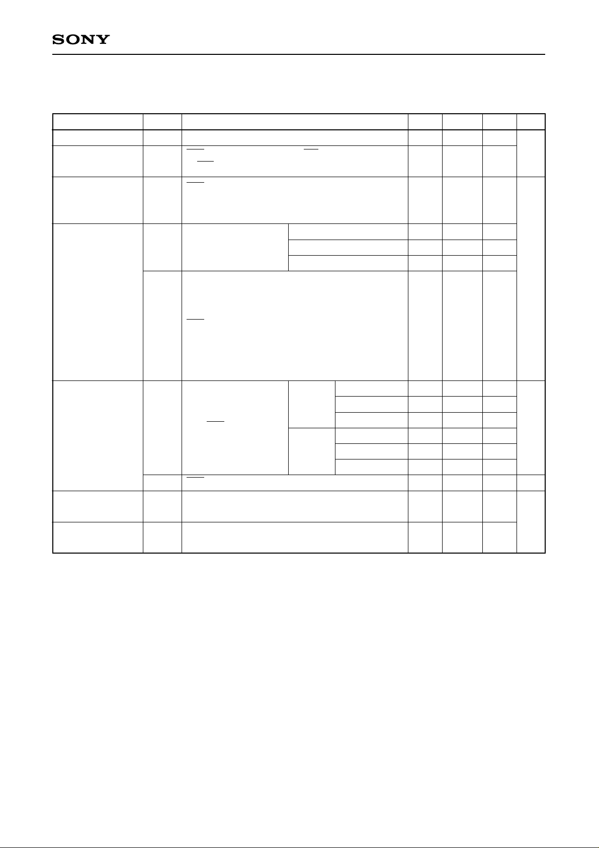
Absolute Maximum Ratings (Ta = 25°C, GND = 0V)
Item Symbol Rating Unit
Supply voltage
Input voltage
Input and output voltage
Allowable power dissipation
Operating temperature
Storage temperature
Soldering temperature
∗
VIN,VI/O = –3.0V Min. for pulse width less than 50ns.
VCC
VIN
VI/O
PD
Topr
Tstg
Tsolder
CXK581000AP
CXK581000ATM/AYM/AM
CXK581000AP
CXK581000ATM/AYM/AM
–0.5 to +7.0
–0.5∗to VCC +0.5
–0.5∗to VCC +0.5
1.0
0.7
0 to +70
–55 to +150
260 • 10
235 • 10
V
W
°C
°C • s
Truth Table
CE1 CE2 OE WE Mode I/O pin VCC Current
H
×
L
L
L
×
L
H
H
H
×
×
H
L
×
×
Not selected
×
Not selected
H
Output disable
H
Read
L
Write
High Z
High Z
High Z
Data out
Data in
ISB1, ISB2
ISB1, ISB2
ICC1, ICC2, ICC3
ICC1, ICC2, ICC3
ICC1, ICC2, ICC3
×: "H" or "L"
DC Recommended Operating Conditions (Ta = 0 to +70°C, GND = 0V)
Item Symbol Min. Typ. Max. Unit
Supply voltage
Input high voltage
Input low voltage
∗
VIL = –3.0V Min. for pulse width less than 50ns.
VCC
VIH
VIL
4.5
2.2
–0.3
5.0
—
∗
—
5.5
VCC +0.3
0.8
V
– 2 –
CXK581000ATM/AYM/AM/AP
Electrical Characteristics
• DC Characteristics (VCC = 5V ±10%, GND = 0V, Ta = 0 to = +70°C)
∗
—
—
1
Max. Unit
1
1
µA
Item Symbol Test conditions Min. Typ.
Input leakage current
Output leakage current
ILI
VIN = GND to VCC
CE1 = VIH or CE2 = VIL or OE = VIH
ILO
or WE = VIL, VI/O = GND to VCC
–1
–1
Operating power
supply current
Average operating
current
Standby current
Output high
voltage
Output low
voltage
∗
1VCC = 5V, Ta = 25°C
∗
2 For -55LL/70LL/10LL
∗
3 For -55SL/70SL/10SL
ICC1
ICC2
ICC3
ISB1
ISB2
VOH
VOL
CE1 = VIL, CE2 = VIH
VIN = VIH or VIL
IOUT = 0mA
Min. cycle
55LL/55SL
Duty = 100% 70LL/70SL
IOUT = 0mA
10LL/10SL
Cycle time 1µs
duty = 100%
IOUT = 0mA
CE1 ≤ 0.2V
CE2 ≥ VCC – 0.2V
VIL ≤ 0.2V
VIH ≥ VCC – 0.2V
∗
2
LL
CE2 ≤ 0.2V
or CE1 ≥ VCC – 0.2V
{
CE2 ≥ VCC – 0.2V
SL
∗
3
CE1 = VIH or CE2 = VIL
IOH = –1.0mA
IOL = 2.1mA
0 to +70°C
0 to +40°C
+25°C
0 to +70°C
0 to +40°C
+25°C
—
—
—
—
—
—
—
—
—
—
—
—
2.4
—
7
45
40
35
10
—
—
0.7
—
—
0.3
0.6
—
—
15
90
70
60
20
20
4
2
12
2.4
1
3
—
0.4
mA
µA
mA
V
– 3 –
I/O Capacitance (Ta = 25°C, f = 1MHz)
Item Symbol Test conditions Min. Typ. Max. Unit
Input capacitance
I/O capacitance
CIN
CI/O
VIN = 0V
VI/O = 0V
—
—
—
—
7
8
pF
Note) This parameter is sampled and is not 100% tested.
AC Characteristics
• AC test conditions (VCC = 5V±10%, Ta = 0 to +70°C)
CXK581000ATM/AYM/AM/AP
Item Conditions
Input pulse high level
Input pulse low level
input rise time
input fall time
Input and output reference level
-55LL/55SL
Output load conditions -70LL/70SL
-10LL/10SL
∗
CL includes scope and jig capacitances.
VIH = 2.2V
VIL = 0.8V
tr = 5ns
tf = 5ns
1.5V
CL∗= 30pF, 1TTL
CL∗= 100pF, 1TTL
• Test circuit
L
C
TTL
– 4 –
 Loading...