

Sony CXJN-5 Service manual
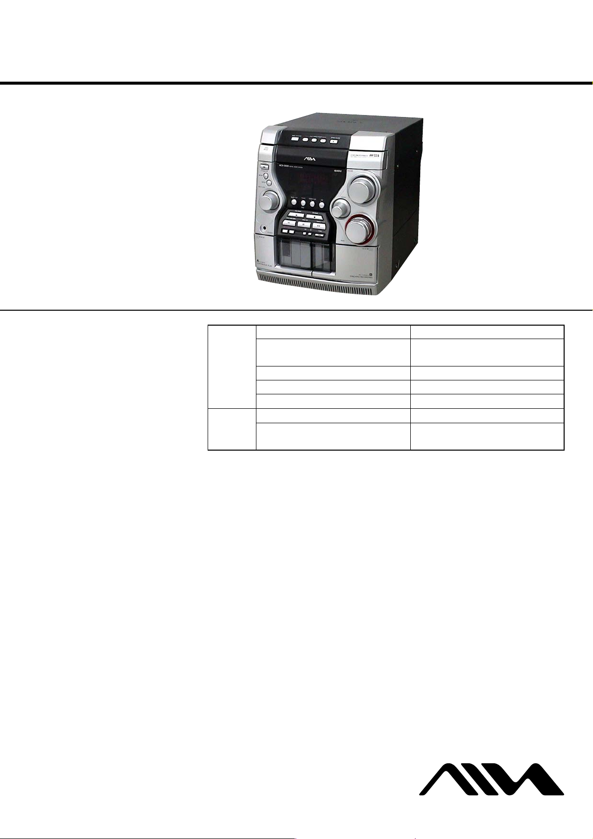
CX-JN5
SERVICE MANUAL
Ver. 1.3 2005.05
CX-JN5 is the amplifier, CD player, tape deck
and tuner section in JAX-N5/PK5.
Model Name Using Similar Mechanism NEW
CD Mechanism Type
CD
Section
Tape deck
Section
Base Unit Name BU-K6BD71A, BU-K6BD72
Optical Block Name KSM-213DCP
Optical Pick-up Name KSS-213D
Model Name Using Similar Mechanism NEW
Tape Transport Mechanism T ype
US Model
Canadian Model
AEP Model
UK Model
E Model
Australian Model
CDM74-K6BD71A, CDM74S-K6BD71A,
CDM74S-K6BD72
CWM43FF13, CWM43FR16,
CWM43FR26
TUNER
FM tuning range
Except CIS model:
CIS model:
FM usable sensitivity (IHF)
Except AEP, UK, CIS models:
AEP, UK models:
CIS model:
FM antenna terminal 75 ohms (unbalanced)
AM tuning range
US, CND, E51, MX models:
AEP, UK, CIS, E, SP, TW models:
KR, AUS models:
AM usable sensitivity 350 µV/m
AM antenna Loop antenna
AMPLIFIER
Power output
US, CND models:
87.5 MHz to 108 MHz
65 MHz to 74 MHz (10 kHz step)
87.5 MHz to 108 MHz (50 kHz step)
dBf
13.2
16.8 dBf
15.3 dBf (65 MHz to 74 MHz)
12.8 dBf (87.5 MHz to 108 MHz)
530 kHz to 1710 kHz (10 kHz step)
531 kHz to 1710 kHz (9 kHz step)
531 kHz to 1602 kHz
531 kHz to 1602 kHz (9 kHz step)
530 kHz to 1710 kHz (10 kHz step)
96 W + 96 W (40 Hz - 20 kHz, THD
less than 1 %, 6 ohms)
120 W + 120 W (1 kHz, THD less
than 10 %, 6 ohms)
SPECIFICATIONS
AEP, UK, CIS models:
Except US, CND, AEP,
UK, CIS models:
Total harmonic distortion
US, CND models:
AEP, UK, CIS models:
Except US, CND, AEP,
UK, CIS models:
Input VIDEO/AUX: 400 mV
Outputs SPEAKERS: 6 ohms or more
CASSETTE DECK
rack format 4 tracks, 2 channels stereo
T
Frequency response 50 Hz – 8 kHz
Recording system AC bias
Rated: 64 W + 64 W (6 ohms, T.H.D.
1 %, 1 kHz/DIN 45500)
Reference: 80 W + 80 W (6 ohms,
T.H.D. 10 %, 1 kHz/DIN 45324)
MUSIC POWER: 195 W +195 W
Rated: 80 W + 80 W (1 kHz, T.H.D.
1 %, 6 ohms )
Reference: 100 W + 100 W (1 kHz,
T.H.D. 10 %, 6 ohms)
0.08 % (45 W, 1 kHz, 6 ohms)
0.08 % (32 W, 1 kHz, 6 ohms, DIN
AUDIO)
0.08 % (40 W, 1 kHz, 6 ohms, DIN
AUDIO)
PHONES: 32 ohms or more
COMPACT DISC DECK RECEIVER
Heads Deck A: playback x 1
CD PLAYER
Laser Semiconductor laser (λ = 780 nm)
D/A converter 1 bit dual
Signal-to-noise ratio 85 dB (1 kHz, 0 dB)
Harmonic distortion 0.05 % (1 kHz, 0 dB)
GENERAL
Power requirements
US, CND, MX models:
AEP, UK, CIS models:
E, E51, SP, TW models:
KR model:
AUS model:
Power consumption
US, CND models:
AEP, UK, CIS models:
Deck B: recording/playback x 1,
erase x 1
Emission duration:
continuous
120 V AC, 60 Hz
230 V AC, 50/60 Hz
110 - 120 V/220 - 240 V AC
(switchable), 50/60 Hz
220 V AC, 60 Hz
240 V AC, 50/60 Hz
100 W
93 W
– Continued on next page –
9-877-250-04 Sony Corporation
2005E05-1 Personal Audio Group
© 2005.05 Published by Sony Engineering Corporation
CX-JN5
r
Except US, CND, AEP, UK,
CIS models:
Power consumption With ECO mode on: 0.25 W
in standby mode With ECO mode off: 20 W
Dimensions (W x H x D) 280 x 330 x 392.5 mm
Weight
US, CND, E51, KR models:
AEP, UK models:
CIS model:
E, MX, SP, TW models:
Specifications and external appearance are subject to change
without notice.
• Abbreviation
AUS : Australian model
CND : Canadian model
E51 : Chilean and Peruvian models
KR : Korean model
MX : Mexican model
SP : Singapore model
TW : Taiwan model
COPYRIGHT
Check copyright laws relevant to recordings from discs, tuner
or tape for the country where the unit is to be used.
Licensed by BBE Sound, Inc. under USP4638258, 5510752
and 5736897.
105 W
1
/8 x 13 x 15 1/2 in.)
(11
8.0 kg (17 lbs 10 oz)
7.2 kg
7.6 kg
7.9 kg
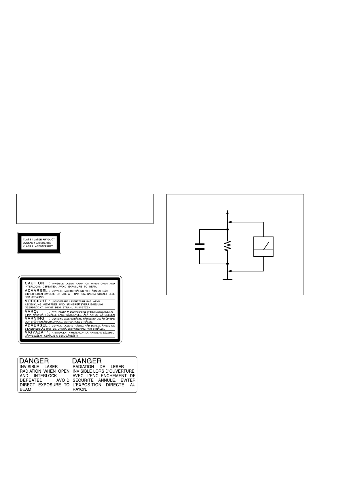
CAUTION
Use of controls or adjustments or performance of procedures
other than those specified herein may result in hazardous radiation exposure.
SAFETY CHECK-OUT
After correcting the original service problem, perform the following safety check before releasing the set to the customer:
Check the antenna terminals, metal trim, “metallized” knobs,
screws, and all other exposed metal parts for AC leakage.
Check leakage as described below.
LEAKAGE TEST
The AC leakage from any exposed metal part to earth ground and
from all exposed metal parts to any exposed metal part having a
return to chassis, must not exceed 0.5 mA (500 microamperes.).
Leakage current can be measured by any one of three methods.
1. A commercial leakage tester, such as the Simpson 229 or RCA
WT -540A. Follo w the manufacturers’ instructions to use these
instruments.
2. A battery-operated AC milliammeter. The Data Precision 245
digital multimeter is suitable for this job.
3. Measuring the voltage drop across a resistor by means of a
VOM or battery-operated AC voltmeter. The “limit” indication is 0.75 V, so analog meters must have an accurate lowvoltage scale. The Simpson 250 and Sanwa SH-63T rd are examples of a passive VOM that is suitable. Nearly all battery
operated digital multimeters that have a 2 V A C range are suitable. (See Fig. A)
To Exposed Metal
Parts on Set
This appliance is classified as
a CLASS 1 LASER product.
The CLASS 1 LASER
PRODUCT MARKING is
located on the rear exterior.
The following caution label is located inside the unit.
AC
1.5 k
0.15 µF
Fig. A. Using an AC voltmeter to check AC leakage.
Ω
Earth Ground
voltmete
(0.75 V)
Notes on chip component replacement
•Never reuse a disconnected chip component.
• Notice that the minus side of a tantalum capacitor may be damaged by heat.
Flexible Circuit Board Repairing
•Keep the temperature of the soldering iron around 270 ˚C during repairing.
• Do not touch the soldering iron on the same conductor of the
circuit board (within 3 times).
• Be careful not to apply force on the conductor when soldering
or unsoldering.
SAFETY-RELATED COMPONENT WARNING!!
COMPONENTS IDENTIFIED BY MARK 0 OR DOTTED
LINE WITH MARK 0 ON THE SCHEMATIC DIAGRAMS
AND IN THE PARTS LIST ARE CRITICAL TO SAFE
OPERATION. REPLACE THESE COMPONENTS WITH
SONY PARTS WHOSE PART NUMBERS APPEAR AS
SHOWN IN THIS MANUAL OR IN SUPPLEMENTS PUBLISHED BY SONY.
2
ATTENTION AU COMPOSANT AYANT RAPPORT
À LA SÉCURITÉ!
LES COMPOSANTS IDENTIFIÉS P AR UNE MARQUE 0
SUR LES DIAGRAMMES SCHÉMATIQUES ET LA LISTE
DES PIÈCES SONT CRITIQUES POUR LA SÉCURITÉ
DE FONCTIONNEMENT. NE REMPLACER CES COMPOSANTS QUE PAR DES PIÈCES SONY DONT LES
NUMÉROS SONT DONNÉS DANS CE MANUEL OU
DANS LES SUPPLÉMENTS PUBLIÉS PAR SONY.

TABLE OF CONTENTS
CX-JN5
Ver 1.1
1. SERVICING NOTES ................................................ 4
2. GENERAL
Location of Controls ....................................................... 7
3. DISASSEMBLY
3-1. Disassembly Flow ........................................................... 9
3-2. Case (SIDE-L/R) ............................................................. 10
3-3. Case (Top) ....................................................................... 10
3-4. Tray Panel........................................................................ 11
3-5. CD Mechanism Deck (CDM74-K6BD71AS,
CDM74S-K6BD71A, CDM74S-K6BD72).................... 11
3-6. Fr ont Panel Section ......................................................... 12
3-7. Mechanical Deck
(CWM43FF13, CWM43FR16, CWM43FR26) ............. 12
3-8. Rear Cabinet Section ...................................................... 13
3-9. PT Board, MAIN Board .................................................. 13
3-10. Table Assy ....................................................................... 14
3-11. Motor (TB) Board ........................................................... 14
3-12. Motor (LD) Board........................................................... 15
3-13. Base Unit (BU-K6BD71A, BU-K6BD72) ..................... 15
3-14. Motor Gear Assy (Sled) (M701), BD Board .................. 16
3-15. Optical Pick-up (KSS-213D).......................................... 16
4. TEST MODE.............................................................. 17
5. ELECTRICAL ADJUSTMENTS
CD Section ...................................................................... 19
7. EXPLODED VIEWS
7-1. Case Section .................................................................... 49
7-2. F ront Panel Section-1...................................................... 50
7-3. F ront Panel Section-2...................................................... 51
7-4. F ront Panel Section-3...................................................... 52
7-5. F ront Panel Section-4...................................................... 53
7-6. Chassis Section ............................................................... 54
7-7. CD Mechanism Deck Section-1 (CDM74-K6BD71AS,
CDM74S-K6BD71A, CDM74S-K6BD72).................... 55
7-8. CD Mechanism Deck Section-2 (CDM74-K6BD71AS,
CDM74S-K6BD71A, CDM74S-K6BD72).................... 56
7-9. CD Mechanism Deck Section-3 (CDM74-K6BD71A,
CDM74S-K6BD71A, CDM74S-K6BD72).................... 57
7-10. Base Unit Section (BU-K6BD71A, BU-K6BD72)........ 58
8. ELECTRICAL PARTS LIST ............................... 59
•Abbreviation
AUS: Australian model
CND : Canadian model
E51 : Chilean and Peruvian models
KR : Korean model
MX : Mexican model
SP : Singapore model
TW : Taiwan model
6. DIAGRAMS
6-1. Block Diagram – CD Section – ..................................... 20
6-2. Block Diagram – TUNER/TAPE/PANEL Section –..... 21
6-3. Block Diagram – AMP/POWER SUPPLY Section – ... 22
6-4. Note for Printed Wiring Boards and
Schematic Diagrams ....................................................... 23
6-5. Printed Wiring Board – BD Section –
(AEP, UK, CIS, E51, MX) .............................................. 24
6-6. Schematic Diagram – BD Section –
(AEP, UK, CIS, E51, MX) .............................................. 25
6-7. Printed Wiring Board – BD Section –
(US, CND, E, SP, TW, KR, AUS) ................................... 26
6-8. Schematic Diagram – BD Section –
(US, CND, E, SP, TW, KR, AUS) ................................... 27
6-9. Printed Wiring Boards – CHANGER Section –............ 28
6-10. Schematic Diagram – CHANGER Section – ................ 29
6-11. Schematic Diagram – MAIN Section (1/4) –................ 30
6-12. Schematic Diagram – MAIN Section (2/4) –................ 31
6-13. Schematic Diagram – MAIN Section (3/4) –................ 32
6-14. Schematic Diagram – MAIN Section (4/4) –................ 33
6-15. Printed Wiring Board – MAIN Section – ...................... 34
6-16. Printed Wiring Board – HP Section – ........................... 35
6-17. Schematic Diagram – HP Section – .............................. 35
6-18. Printed Wiring Board – PANEL Section – .................... 36
6-19. Schematic Diagram – PANEL Section – ....................... 37
6-20. Printed Wiring Boards – KEY Section – ....................... 38
6-21. Schematic Diagram – KEY Section – ........................... 39
6-22. Printed Wiring Board – PT Section –
(Except E, E51, SP, TW)................................................. 40
6-23. Schematic Diagram – PT Section –
(Except E, E51, SP, TW)................................................. 41
6-24. Printed Wiring Board – PT Section –
(E, E51, SP, TW) ............................................................. 42
6-25. Schematic Diagram – PT Section –
(E, E51, SP, TW) ............................................................. 43
6-26. IC Pin Function Description ........................................... 47
3

CX-JN5
Ver 1.1
SECTION 1
SERVICING NOTES
NOTES ON HANDLING THE OPTICAL PICK-UP
BLOCK OR BASE UNIT
The laser diode in the optical pick-up block may suffer electrostatic break-down because of the potential difference generated
by the charged electrostatic load, etc. on clothing and the human
body.
During repair, pay attention to electrostatic break-down and also
use the procedure in the printed matter which is included in the
repair parts.
The flexible board is easily damaged and should be handled with
care.
NOTES ON LASER DIODE EMISSION CHECK
The laser beam on this model is concentrated so as to be focused
on the disc reflective surface by the objective lens in the optical
pick-up block. Therefore, when checking the laser diode emission, observe from more than 30 cm away from the objectiv e lens.
LASER DIODE AND FOCUS SEARCH OPERATION
CHECK
Carry out the “S curve check” in “CD section adjustment” and
check that the S curve waveforms is output three times.
UNLEADED SOLDER
Boards requiring use of unleaded solder are printed with the leadfree mark (LF) indicating the solder contains no lead.
(Caution: Some printed circuit boards may not come printed with
the lead free mark due to their particular size)
: LEAD FREE MARK
Unleaded solder has the following characteristics.
• Unleaded solder melts at a temperature about 40 ˚C higher than
ordinary solder.
Ordinary soldering irons can be used but the iron tip has to be
applied to the solder joint for a slightly longer time.
Soldering irons using a temperature regulator should be set to
about 350 ˚C.
Caution: The printed pattern (copper foil) may peel away if the
heated tip is applied for too long, so be careful!
• Strong viscosity
Unleaded solder is more viscou-s (sticky, less prone to flow)
than ordinary solder so use caution not to let solder bridges occur such as on IC pins, etc.
• Usable with ordinary solder
It is best to use only unleaded solder but unleaded solder may
also be added to ordinary solder.
• MODEL IDENTIFICATION
– Back Panel –
PART No.
MODEL PART No.
US model 4-245-154-0
Chilean and Peruvian models 4-245-154-2
CIS model 4-245-154-4
E, Singapore and Taiwan models 4-245-154-6[]
Korean and Australian models 4-245-154-8
AEP and UK models 4-245-280-0
Mexican model (made in Mexico) 4-245-280-3
Mexican model (made in China) 4-245-280-4
Canadian model 4-245-280-5
[]
[]
[]
[]
[]
[]
[]
[]
4
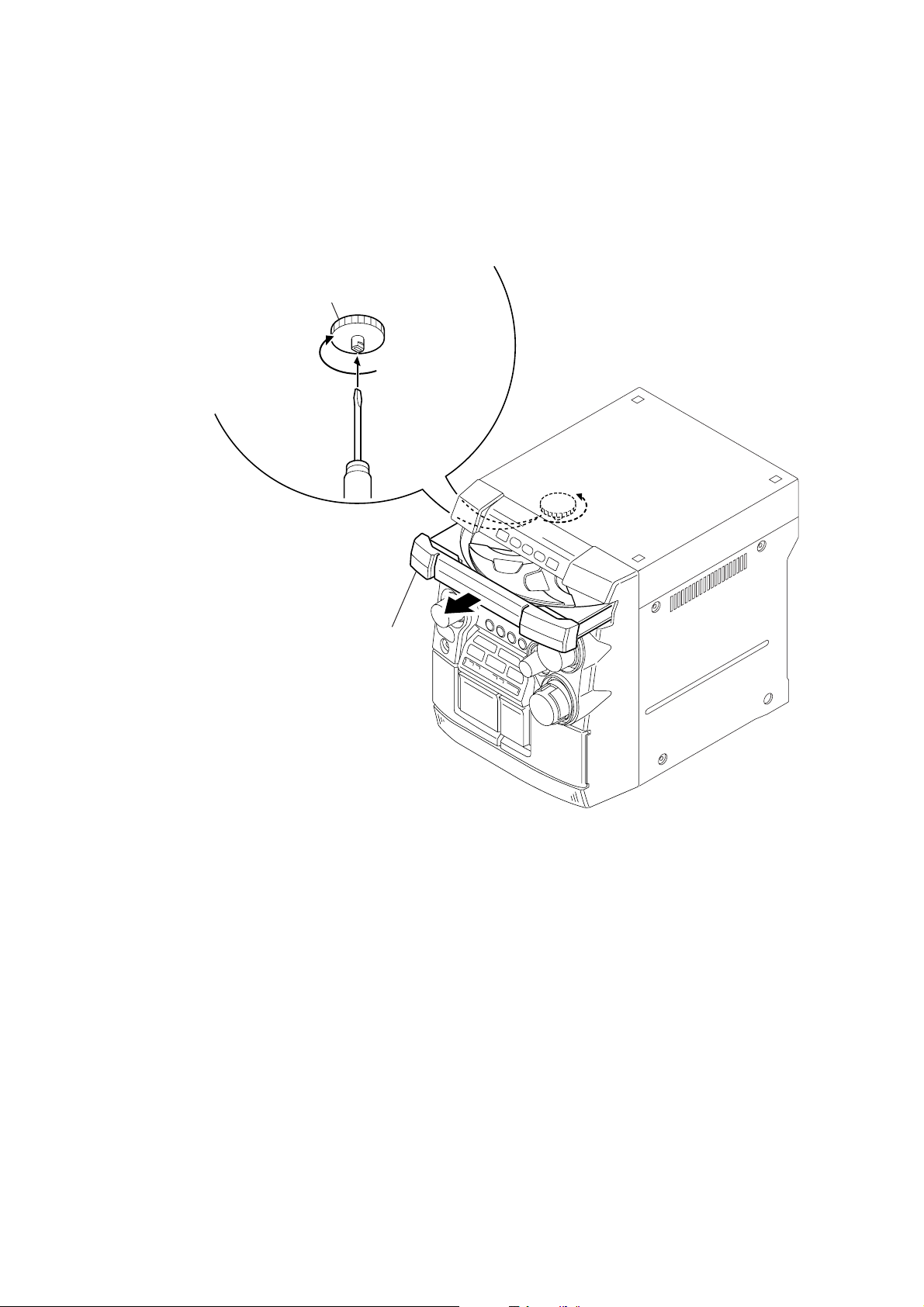
HOW TO OPEN THE DISC TRAY WHEN POWER SWITCH TURNS OFF.
1
Remove the case (side-L).
2
Turn the loading gear in the direction of arrow A.
A
CX-JN5
3
Pull-out the disc tray.
5
CX-JN5
SERVICE POSITION
– CD mechanism deck –
main board (CN691)
– Tape mechanism deck –
Connect wire (flat type) (19 core) to
main board (CN691) and BD board (CN710).
BD board (CN710)
panel board (CN601)
Connect wire (flat type) (13 core) to
panel board (CN601) and mechanical deck.
main board (CN301)
6
M
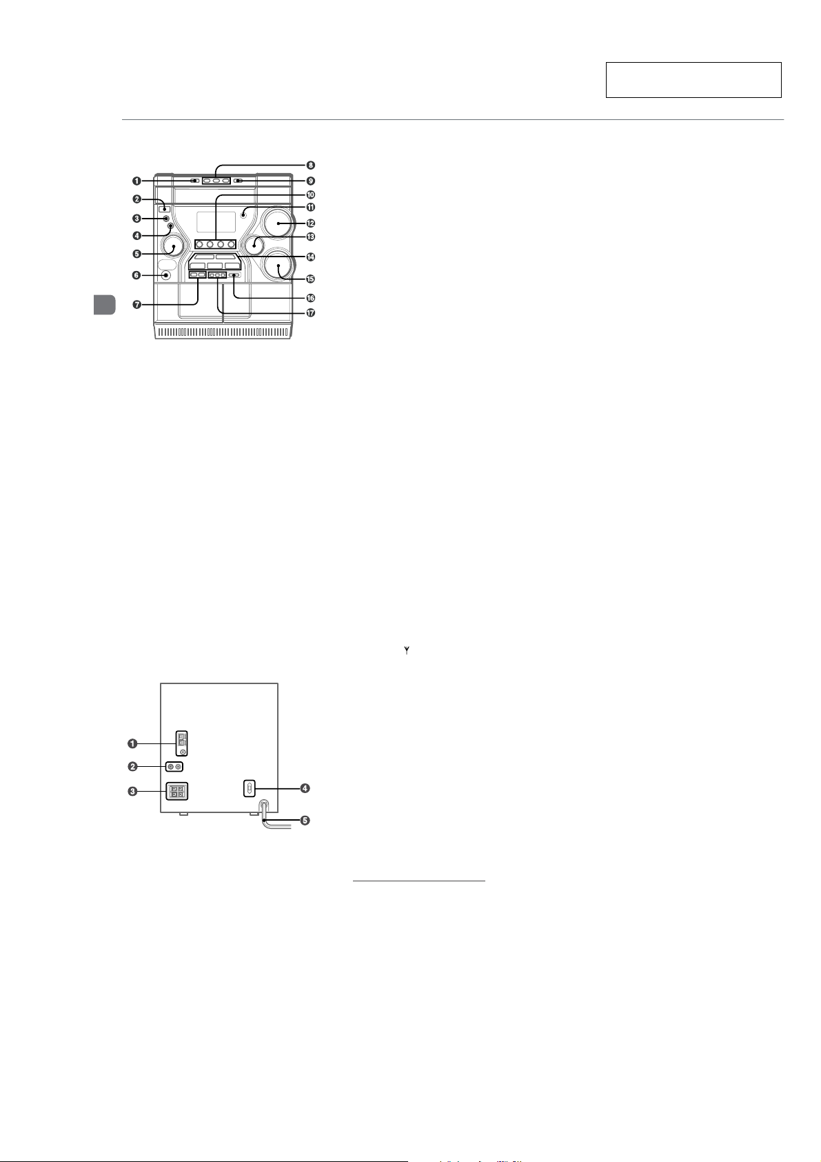
• LOCATION OF CONTROLS
SECTION 2
GENERAL
CX-JN5
Ver 1.1
This section is extracted from
instruction manual.
Main unit: front
En
1 DISC CHANGE
Rotates the CD trays.
2 POWER 6STANDBY/ON
Switches the unit on and off (standby).
The red indicator flashes when receiving a signal from
the remote.
3 MODE
Selects various modes (ECO and Repeat/Shuffle/
Programmed playback, etc.) when used in combination
with ENTER and MULTI JOG.
4 ENTER
Fixes the modes and the time (ECO, Repeat/Shuffle/
Programmed playback, clock, and timer, etc.) when used
in combination with ENTER and MULTI JOG.
5 MULTI JOG
When used in combination with ENTER and MULTI JOG,
CD: selects a track and Repeat/Shuffle/Programmed
playback.
Tuner: selects a preset station.
Tape: selects a reverse mode and specifies tape length.
Clock and Timer: sets the time.
i-Bass: selects a frequency range.
Spectrum analyzer, ECO and Dimmer: selects the mode.
6 PHONES jack
Plug in here an optional headphones set with a mini
stereo plug (ø3.5 mm). Speaker output is canceled.
7 SYNC DUB
Starts dubbing a whole tape.
wREC/REC MUTING
Starts recording.
8 DISC DIRECT PLAY 1-3
Selects a disc.
9 zOPEN/CLOSE
Opens or closes the disc compartment.
0 TAPE A/B
Selects Tape function, and deck A or B.
TUNER/BAND
Selects Tuner function and the radio band.
VIDEO/AUX
Selects the function of external equipment connected to
VIDEO/AUX jacks.
CD
Selects CD function.
! Remote sensor
Receives a signal from the remote.
@ VOLUME
Adjusts the volume.
# TREBLE
Enhances high frequency sound.
$ dDIR (TAPE B) /PRESET
When the unit is turned off: activates or deactivates
DEMO.
CD and Tape: starts playback.
Tuner: tunes into a preset station.
sSTOP/CLEAR
CD and Tape: stops playback.
Tuner: clears a station preset.
fTUNING DOWN, gTUNING UP
CD: sear ches a track in fast
playback when held down.
Tape: fast or rewinds the tape.
forward
Tuner: manually tunes down or up within the band.
aPAUSE/SET
CD and Tape: pauses playback.
Tuner: stores the received station into preset.
% BASS
Emphasizes low frequency sound.
^ i-Bass
Produces rich and clear low frequency sound.
& DISPLAY
Displays the time and the remaining time for CD.
ALBUM k, i (AEP, UK, CIS, Chilean,
Peruvian and Mexican models)
Selects a previous album or a succeeding album
MP3-CDs.
forward
or fast reverse
ain unit: rear
1 AM LOOP,
Plug in the supplied AM and FM antennas here.
2 VIDEO/AUX jacks
Accepts analog sound signals from external equipment.
Connect using an optional connecting cable with RCA
phono plugs (red plug to R jack, white plug to L jack).
Refer also to the operating instructions of your equipment.
To switch function to external input, press VIDEO/AUX.
Tip:
To change the displayed name for this function, turn the
unit on, then hold down VIDEO/AUX and press POWER
on the unit. Repeat the procedure to select "VIDEO",
"AUX" or "TV".
3 # SPEAKER terminals
Connect the speaker cord of the supplied front speakers
here.
4 AC voltage selector (E, Chilean, Peruvian, Singapore, Taiwan)
Switches AC voltage between 110 - 120V and 220 - 240V .
Make sure it matches your local voltage.
5 AC power cord
FM 75 Ω terminals
7
CX-JN5
Ver 1.1
Remote control
Refer to the pages indicated in parentheses for details.
Buttons with the same or similar names with
the main unit basically have the same function.
1 POWER
2 1-0/10, +10
CD: selects a CD track of the specified number.
Tuner: tunes in to the station with the specified pr eset
number .
The numbered buttons take on these functions
below when pressed with SHIFT held down
EDIT
Enters AI Edit Recording or Programmed Edit Recording
mode when pressed in stop mode.
BAND
Selects Tuner function and the radio band.
TAPE A/B
SPECTRUM
Changes the spectrum analyzer display.
TUNER MODE
Switches between stereo or monaural FM reception.
3 r, t
CD: selects a track.
Tuner: selects a preset station.
Tape: specifies tape length.
BASS and TREBLE: adjusts the level.
Clock and Timer: sets the time.
4 ALBUM M, N
Selects a previous album or a succeeding album.
5 PLAY MODE
CD: selects Shuffle, Programmed playback, etc.
Tape: selects a r everse mode (deck B only).
REPEAT
Enters CD repeat playback mode.
ENTER
6 CLOCK/TIMER/SET
Enters timer setting mode.
CLOCK/TIMER/SELECT
Selects timer playback, timer recording or timer off.
7 DISPLAY
SHIFT
8
:
Hold down when pressing a numbered button to change
its function to that printed above the number.
e.g.)
"Press SHIFT+BAND on the remote" indicates "Hold
down SHIFT and press '2' (BAND)". Doing so makes you
be able to select Tuner function and the radio band.
9 FUNCTION
Switches the active function among CD, T APE, TUNER
and VIDEO (AUX or TV).
0 DISC SKIP
Select a disc.
! c/d
When the unit is turned off: activates or deactivates
DEMO.
CD and Tape: starts playback.
s
CD and Tape: stops playback.
f,g
CD: searches a track in fast for war d or fast reverse
playback when held down.
Tape: fast for wards or rewinds the tape.
Tuner: manually tunes down or up within the band.
a
CD and Tape: pauses playback.
@ SLEEP
Switches the sleep-timer on/off and selects the duration.
# VOLUME ( +, -)
Adjusts the volume.
$ SOUND
Selects BASS or TREBLE setting mode
CLEAR
Clears a track of the CD programmed playback and
Radio preset station.
Note
The button not explained above (KARAOKE) does not
operate for US, Canadian, AEP, UK and CIS models.
The buttons not explained above (
do not operate for US, Canadian, E, Singapore, Taiwan, Korean
and Australain models.
ALBUM M, N
)
En
Setting the clock
Use the remote.
1
Press CLOCK/TIMER/SET.
Go to step 3 when the time appears and the 'hour' flashes.
2
Press r or t repeatedly until "
SET
" appears in the display and then press
ENTER.
3
Press r or t repeatedly to set the hour
and then press ENTER.
4
Press r or t repeatedly to set the minute
and then press ENTER.
The time display stops flashing and the clock starts from
00 seconds.
•MULTI JOG is also available in place of r or t.
To display the time
Press DISPLAY on the remote. The time will be displayed for
6 seconds.
Tip:
"AM 12:00" indicates midnight and "PM 12:00" noon.
If "- -:- -" appears when the unit is turned off
There has been a power interruption. Re-set the clock.
CLOCK
En
8
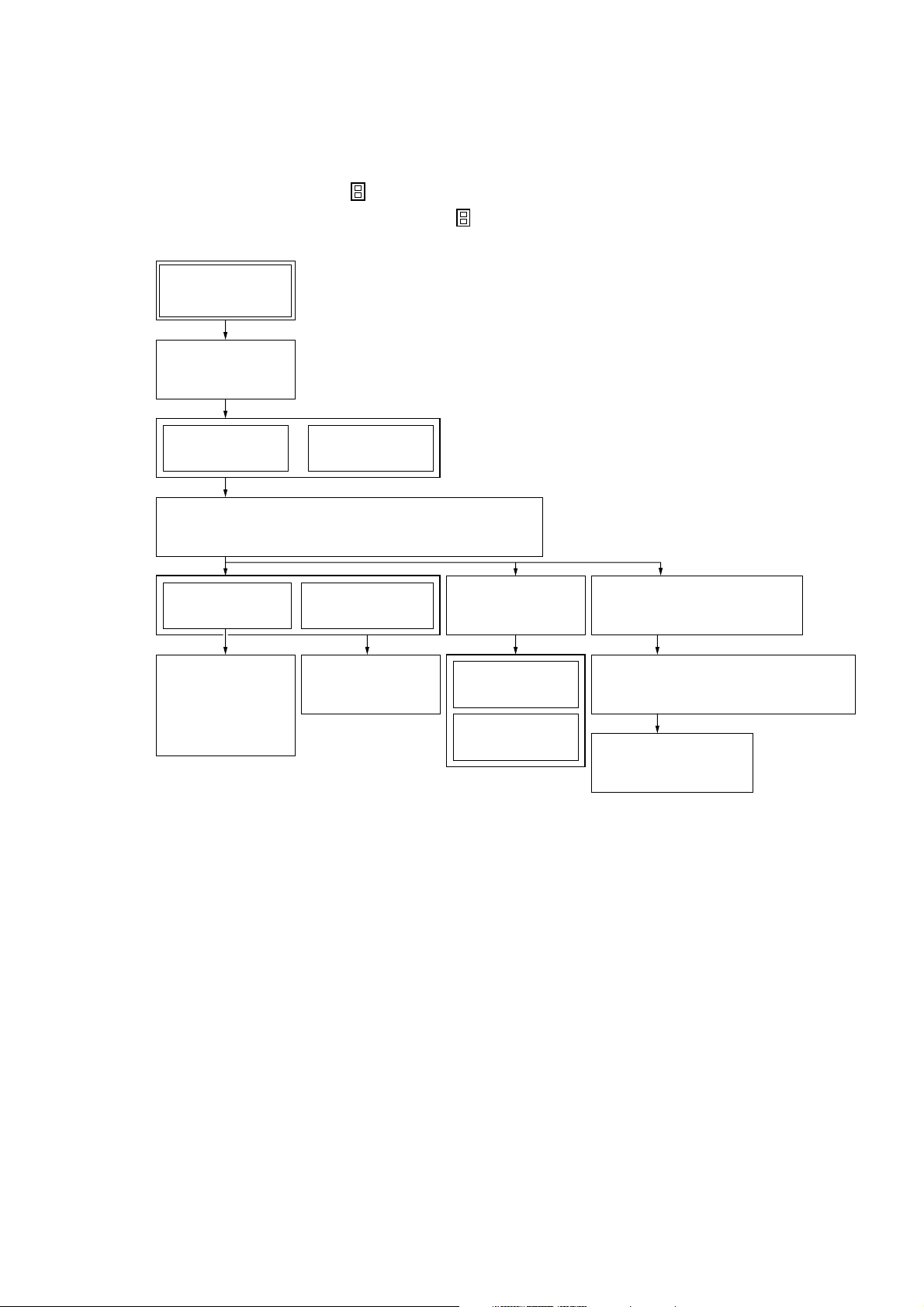
• This set can be disassembled in the order shown below.
Set
3-2. CASE
(SIDE-L/R)
(Page 10)
3-3. CASE (TOP)
(Page 10)
3-4. TRAY PANEL
(Page 11)
3-6. FRONT PANEL
SECTION
(Page 12)
3-8. REAR CABINET
SECTION
(Page 13)
3-7. MECHANICAL
DECK
(CWM43FF13,
CWM43FR16,
CWM43FR26)
(Page 12)
3-9. PT BOARD,
MAIN BOARD
(Page 13)
3-14. MOTOR GEAR ASSY (SLED) (M701),
BD BOARD
(Page 16)
3-15. OPTICAL PICK-UP
(KSS-213D)
(Page 16)
3-13. BASE UNIT
(BU-K6BD71A, BU-K6BD72)
(Page 15)
3-10. TABLE ASSY
(Page 14)
3-11. MOTOR (TB)
BOARD
(Page 14)
3-12. MOTOR (LD)
BOARD
(Page 15)
3-5. CD MECHANISM DECK
(CDM74-K6BD71A, CDM74S-K6BD71A, CDM74S-K6BD72)
(Page 11)
Note 1: The process described in can be performed in any order.
Note 2: Without completing the process described in , the next process can not be performed.
3-1. DISASSEMBLY FLOW
CX-JN5
SECTION 3
DISASSEMBLY
9

CX-JN5
s
w
Note: Follow the disassembly procedure in the numerical order given.
3-2. CASE (SIDE-L/R)
5
case (side-L)
1
two case screws
3
2
two screws
(BVTP3
×
10)
2
two screws
(BVTP3
×
10)
1
case screw
3-3. CASE (TOP)
4
case (top)
4
2
claw
3
1
3
4
case screw
1
5
case (side-R)
1
two screws
(BVTP3 × 10)
two case screw
10
2
claw
2
cla
2
claw

3-4. TRAY PANEL
)
1
Turn the loading gear
in the direction of arrow
2
Pull-out the disc table.
4
tray panel
A
3
four claws
CX-JN5
Ver 1.1
.
A
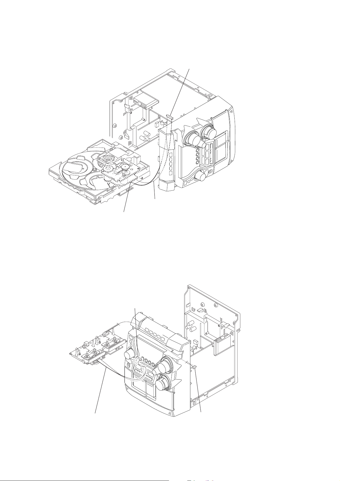
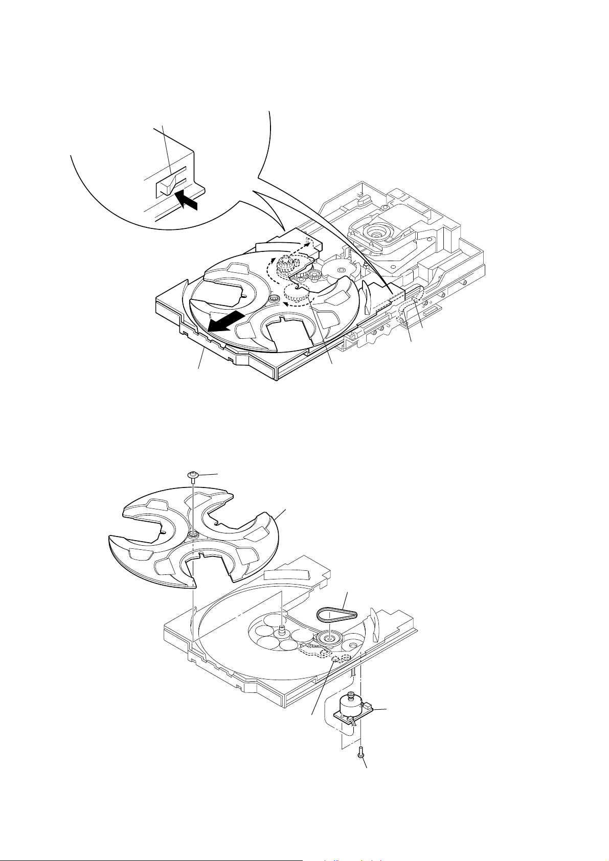
3-5. CD MECHANISM DECK (CDM74-K6BD71AS, CDM74S-K6BD71A, CDM74S-K6BD72)
5
CD mechanism deck
(CDM74-K6BD71AS,
CDM74S-K6BD71A,
CDM74S-K6BD72)
1
wire (flat type) (19 core
(CN691)
2
connector
3
screw
(BVTP3 × 10)
(CN701)
4
two screws
(BVTP3 × 10)
3
screw
(BVTP3 × 10)
11
CX-JN5
Ver 1.1
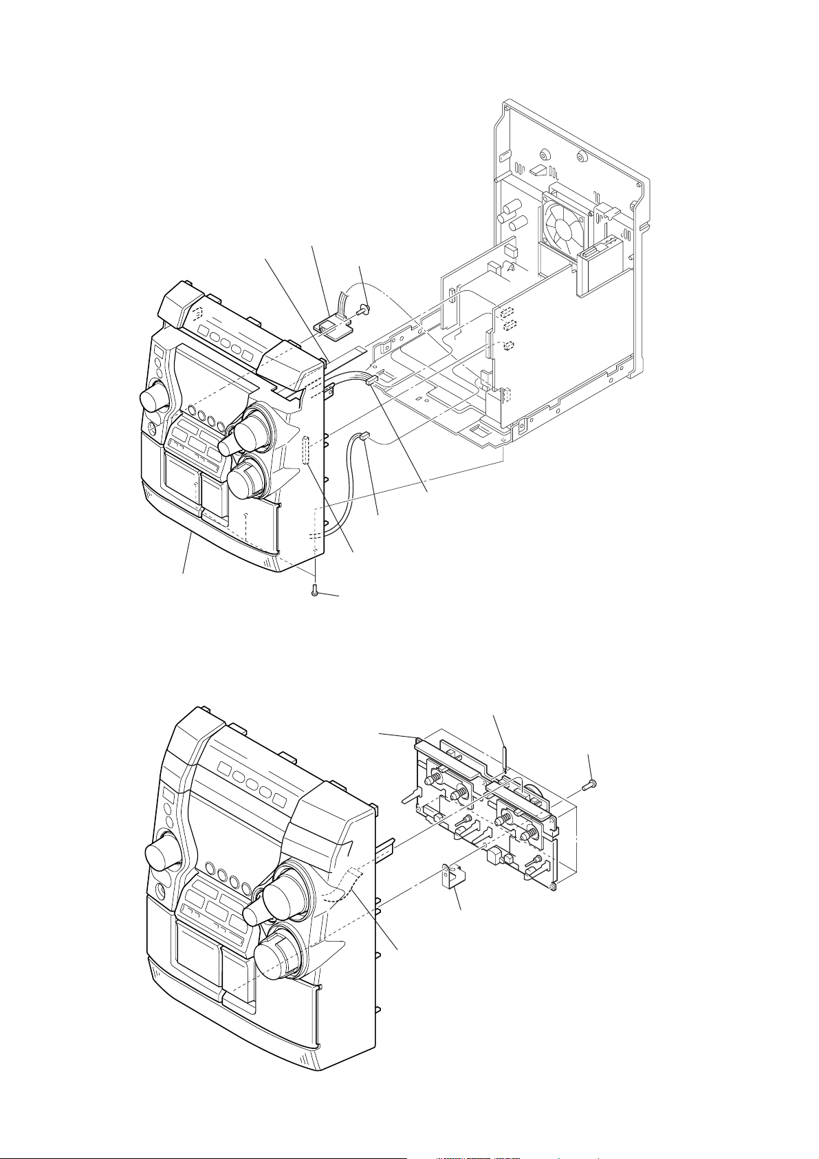
3-6. FRONT PANEL SECTION
3
wire (flat type) (11 core)
(CN694)
2
headphone board
1
screw
(BVWHTP)
4
connector
×
(CN302)
10)
7
front panel section
4
6
connector
(CN601)
5
three screws
(BVTP3
connector
(CN301)
3-7. MECHANICAL DECK (CWM43FF13, CWM43FR16, CWM43FR26)
4
mechanical deck
(CWM43FF13,
CWM43FR16,
CWM43FR26)
3
clamp
2
six screws
(BVTP3
×
10)
12
5
ground mechanical plate
1
wire (flat type) (13 core)

3-8. REAR CABINET SECTION
)
1
wire (flat type)
(CN801) (11 core: EXCEPT AEP, UK)
(CN802) (15 core: AEP, UK)
3
rear cabinet section
2
2
three screws
(BVTP3
screw
(BVTP3
×
CX-JN5
Ver 1.1
×
10
10)
3-9. PT BOARD, MAIN BOARD
•
Abbreviation
AUS: Australian model
CND : Canadian model
E51 : Chilean and Peruvian models
(US, CND, AEP, UK, CIS, MX, KR, AUS)
6
8
two screws
(ITC4
9
PT board
screw
(BVTP3
×
10)
×
8)
7
Remove the PWB PT HLDR
in the direction of the arrow.
8
two screws
(ITC4
A
4
5
×
8)
screw
(BVTT3
clamp
KR : Korean model
MX : Mexican model
(E, E51, SP, TW)
7
×
8)
5
screw
(BVTP3
8
PT board
A
3
SP : Singapore model
TW : Taiwan model
4
screw
×
A
8)
7
two screws
(ITC4
×
(BVTT3
6
Remove the PWB PT HLDR
two screws
×
8)
(ITC4
×
10)
connector
(CN090) (E, E51, SP, TW)
(CN091) (US, CND, AEP, UK, CIS, MX, KR, AUS)
1
in the direction of the arrow.
screw (BVTT3 × 8)
8)
1
two screws
(BVTT3
2
×
8)
main board
13
CX-JN5
)
d
Ver. 1.3
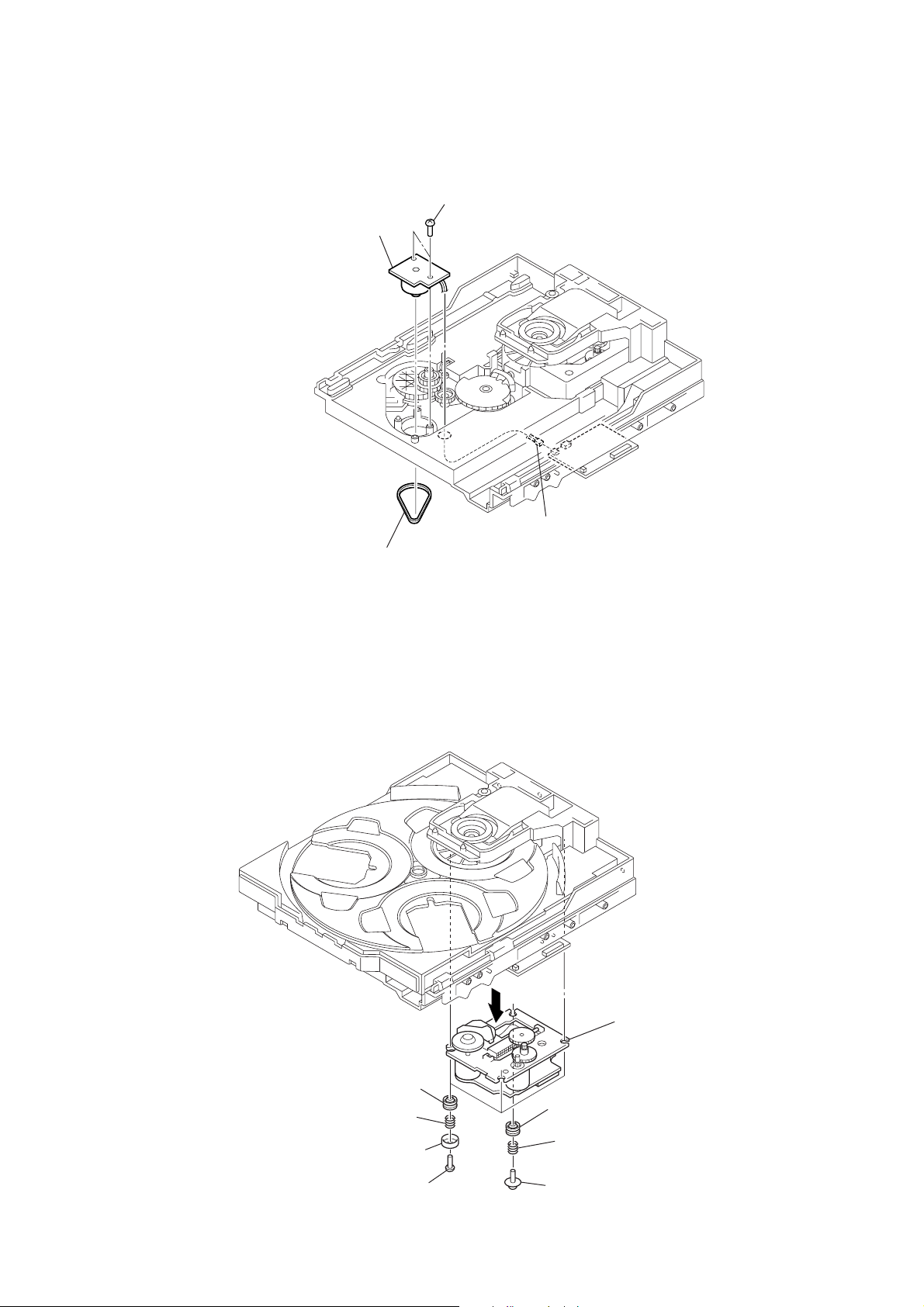
3-10. TABLE ASSY
two claws
5
A
2
Pull-out the table assy.
6
table assy
3-11. MOTOR (TB) BOARD
1
screw
(PTPWH M2.6)
2
tray
1
Turn the loading gear
in the direction of arrow
3
belt (table)
4
hook
3
wire (flat type) (5 core
(CN702)
A
.
14
4
connector
(CN731)
6
5
two screws
(BTTP M2.6)
motor (TB) boar
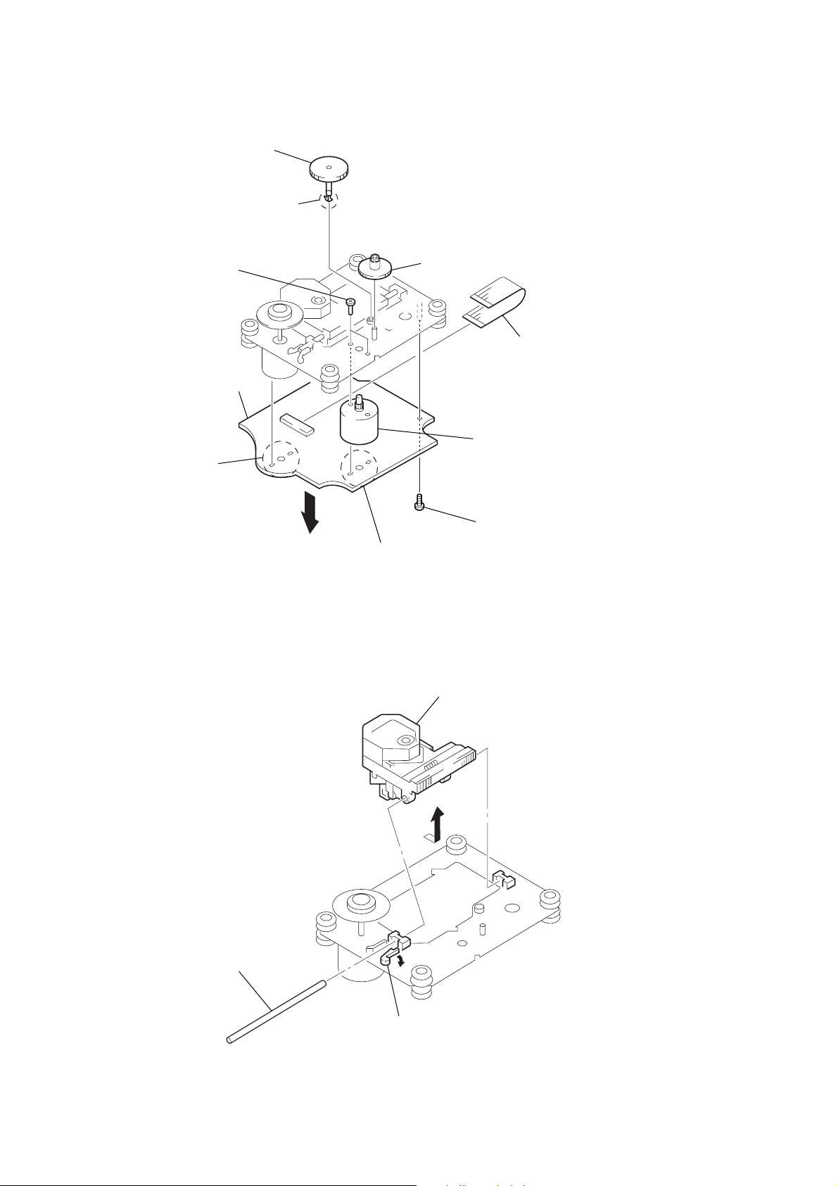
3-12. MOTOR (LD) BOARD
4
motor (LD) board
3
two screws
(BTTP M2.6)
CX-JN5
Ver 1.1
1
belt (loading)
3-13. BASE UNIT (BU-K6BD71A, BU-K6BD72)
2
connector
(CN704)
7
three insulators
3
three coil springs
(insulator)
2
three stoppers (BU)
1
three screws
(BTTP M2.6)
6
9
8
insulator
5
coil spring
(insulator)
4
screw
(PTPWH M2.6)
base unit
(BU-K6BD71A, BU-K6BD72)
15
CX-JN5
)
3-14. MOTOR GEAR ASSY (SLED) (M701), BD BOARD
7
gear (A)
6
claw
2
two screws
×
3)
(P2
qa
BD board
1
Remove two
solders.
8
gear (B)
5
wire (flat type) (16 core
(CN708)
0
motor gear assy (SLED)
(M701)
3-15. OPTICAL PICK-UP (KSS-213D)
4
9
Remove two solders.
3
B
3
screw (P2.6 × 6)
Remove the optical pick-up
(KSS-213D) in the direction
of arrow
B
.
16
2
sled shaft
A
1
Slide the lever
in the direction of arrow
A
.

SECTION 4
TEST MODE
CX-JN5
MC COLD RESET
• The cold reset clears all data including preset data stored in the
RAM to initial conditions. Execute this mode when returning
the set to the customer.
Procedure:
1. In the standby status, while pressing the x button, press the
[POWER] button.
2. The set is reset, then becomes standby status.
GC TEST MODE
Procedure:
1. Press the [POWER] button to turn the power on.
2. While pressing the x button, press the [POWER] button for
5 seconds.
3. It change displays in order of model type, version and suffix at
2 seconds interval, then the display is back to normal status.
AMP TEST MODE
Procedure:
1. In the status where AC plug is disconnected, while pressing
the [VIDEO/AUX] button, connect the AC plug to turn the
power on. Then enter the AMP test mode and display “AMP
TEST”.
2. If turn the [VOLUME] knob clockwise, it displays “V OLUME
MAX”, and if turn the knob counterclockwise, it displays
“VOLUME 0”.
3. If the [TREBLE] and [BASS] knobs are turned clockwise or
counterclockwise, it change displays in order of “EQ MAX”,
“EQ MIN” and “EQ FLAT”.
4. To release from this mode, disconnect the AC plug and turn
the power off.
CHANGE-OVER OF AM TUNER STEP BETWEEN
9 kHz AND 10 kHz
(Except AEP, UK and CIS models)
•A step of AM channels can be changed o ver between 9 kHz and
10 kHz.
Procedure:
1. Press the [POWER] button to turn the power on.
2. While pressing the [TUNER] button, press the [POWER] but-
ton to the display on fluorescent indicator tube changes to “AM
530 kHz” (10 kHz step) or “AM 531 kHz” (9 kHz step), and
thus the channel step is changed over.
FUNCTION CHANGE MODE
• Select either TV, VIDEO or AUX (MD) of the external function
input.
Procedure:
1. Press the [POWER] button to turn the power on.
2. While pressing the [VIDEO/AUX] button, press the [POWER]
button.
3. Each time this operation is operated, it change displays in or-
der of “TV”, “VIDEO” and “AUX”.
DISC TRAY LOCK
Procedure:
1. Press the
2. While pressing the x button, press the [ OPEN/CLOSE]
button for 5 seconds.
3. The message “LOCKED” is displayed and the tray is locked.
(Even if exiting from this mode, the tray is still locked)
4. To release this lock, while pressing the x button, press the
[ OPEN/CLOSE] button for 5 again.
Z
5. The message “UNLOCKED” is displayed and the tray is unlocked.
CD REPEAT 5 LIMIT CANCEL MODE
• Number of repeat for CD playback is 5 times when the repeat
mode is “REPEAT”. This mode enables CD to repeat playback
for limitless times.
Procedure:
1. Press the [POWER] button to turn the power on.
2. In the repeat on status, while pressing the x button, press the
[POWER] button to turn the power on.
Z
[CD] button to enter the CD repeat 5 limit cancel mode and
repeat mark blinks on the fluorescent indicator tube.
3. To release this mode, press the [POWER] button to turn the
power off.
17

CX-JN5
CD TEST MODE
•This mode can run the CD sled motor freely. Use this mode, for
instance, when cleaning the pickup.
Procedure:
1. In the status where AC plug is disconnected, while pressing
the [CD] button, connect the AC plug to turn the power on.
2. When enter this mode, it displays “CD TEST” and few sec-
onds later, all segments turn on of the fluorescent indicator
tube.
3. To release from this mode, disconnect the AC plug and turn
the power off.
In this mode, it operates as following table.
Button Operation Purpose of use
M Move the pick-up to outside track Sled circuit check
m Move the pick-up to inside track Tracking circuit check
Mechanism operation check
Optical pick-up check
N Playback a CD Servo block check
If it cannot focus on, it continuous focus search
x When playback a CD: stop playback APC circuit check
When stop a CD: Laser current measure
display “READING” (blink) Focus search waveform check
continuous laser diode on Tracking balance check
continuous focus search (not made focus on)
X Pause, Tracking servo off
(ignore CLV error)
18

p
p
SECTION 5
ELECTRICAL ADJUSTMENTS
CX-JN5
Ver 1.1
CD SECTION
Note:
1. CD Block is basically designed to operate without adjustment. Therefore,
check each item in order given.
2. Use YEDS-18 (3-702-101-01) unless otherwise indicated.
3. Use an oscilloscope with more than 10MΩ impedance.
4. Clean the object lens by an applicator with neutral detergent when the
signal level is low than specified value with the following checks.
S-CURVE CHECK
Oscilloscope
BD board
TP(FE)
TP(VC)
Procedure :
1. Connect an oscilloscope to TP (FE) and TP (VC).
2. Turn the power on.
3. Load a disc (YEDS-18) and actuate the focus search. (In
consequence of open and close the disc tray, actuate the focus
search)
4. Confirm that the oscilloscope waveform (S-curve) is
symmetrical between A and B. And confirm peak to peak level
within 3 ± 0.5 Vp-p.
Note: Clear RF signal waveform means that the shape “ ◊ ” can be clearly
distinguished at the center of the waveform.
RF signal waveform
VOLT/DIV : 200mV
TIME/DIV : 500ns
±
level : 1.3
0.3Vp-
Connecting Location: BD board
– BD Board (Conductor side) –
(AEP, UK, CIS, Chilean, Peruvian, Mexican models)
TP (RF)
IC721
TP (VC)
TP (FE)
S-curve waveform
symmetry
A
±
within 3
B
Note: •Try to measure several times to make sure than the ratio
of A : B or B : A is more than 10 : 7.
•Take sweep time as long as possible and light up the
brightness to obtain best waveform.
0.5Vp-
RF LEVEL CHECK
BD board
TP(RF)
TP(VC)
Procedure :
1. Connect an oscilloscope to TP (RF) and TP (VC).
2. Turn the power on.
3. Load a disc (YEDS-18) and playback.
4. Confirm that oscilloscope waveform is clear and check if RF
signal level is correct or not.
oscilloscope
– BD Board (Conductor side) –
(US, Canadian, E, Singapore, Taiwan, Korean,
Australian models)
TP (VC)
TP (RF)
TP (FE)
IC721
1919
CX-JN5
SECTION 6
DIAGRAMS
6-1. BLOCK DIAGRAM – CD Section –
OPTICAL PICK-UP
BLOCK
(KSM-213DCP)
A
DETECTOR
A
D
C
B
E
F
LASER DIODE
PD
D
C
I-V AMP
B
E
F
LD
LD
PD
AUTOMATIC
POWER CONTROL
Q701
8
7
9
10
80
79
(AEP, UK, CIS, Chilean, Peruvian, Mexican)
CD DSP
(US, Canadian, Saudi Arabia, Singapore, Taiwan, Korean, Australian)
IC721
FIN2
RF
PH, BH
A/D
CONVERTER
SERVO
PROCESSOR
D/A
CONVERTER
4
FIN1
TIN1
TIN2
LDD
LDS
RF AMP
APC
TBAL
EQ,
AGC
LCHO
EFMIN
3
ERROR
CORRECT
D/A
CONVERTER
EXTERNAL
AUDIO IN
SERIAL OUT
CLOCK
GENERATOR
FSX/16MIN
RCHO
ASDFIN
ASDACK
ASLRCK
DATA
DATACK
LRSY
EFLG
C2F
16MOUT
XIN
XOUT
42
45
57
56
55
60
59
58
53
52
50
26MP3RES
54
49
48
16.9344MHz
X701
R-CH
(AEP, UK, CIS, Chilean, Peruvian, Mexican)
2 ADDATA
3 ADBCK
4 ADLRCK
79 DATAIN
80 DATACK
1 LRSY
MP3 DECODER
IC801
5 C2FIN
9 CKOUT
78 RESB
7 CKIN
73 CMDOUT
74 CMDIN
75 CL
CE
76 66
FSYNC
MDATA0
– MDATA15
MADRS0
– MADRS8
23-30, 33-4060-53, 50
MEMORY
2-5, 7-10,
31-34, 36-39
A0 – A8
16-19, 22-26
27 OE45OEB
13 WE42WEB
14 RAS41RASB
29 LCAS43CASLB
28 UCAS44CASUB
IC802
I/O1 – I/O16
CD
(Page 22)
A
2-AXIS
DEVICE
(FOCUS)
(TRACKING)
M701
(SLED)
M702
(SPINDLE)
S701
(LIMIT)
FOCUS/TRACKING COIL DRIVE,
SPINDLE/SLED MOTOR DRIVE
VO3(+)
18
17 VO3(–)
11 VO2(+)
12 VO2(–)
26 VO4(+)
27 VO4(–)
2 VO1(+)
1 VO1(–)
IC722
(AEP, UK, CIS, Chilean, Peruvian, Mexican)
US, Canadian, Saudi Arabia, Singapore,
Taiwan, Korean, Australian
M
M
FOIN
70 LIMIT SW
20TIN
10
25SLIN
3SPIN
7LDS
TDO
FDO23SLDO22SPDO25CONT4
20
21
DO
64
DI
63
WRQ
CL
62
CE
61
65
67DRF
66RES
COMMAND
INTERFACE
• R-ch is omitted due to same as L-ch.
• SIGNAL PATH
: CD
99 CD DO
98 CD DI
100 C D CLK
5 CD CE
97 CD WRQ
95 CD DRF
4 CD RESET
M751
(LOADING)
M741
(TABLE)
106
MP3 CE
SYSTEM CONTROLLER
IC901 (1/2)
LOADING MOTOR DRIVE
M
M
MP3 SYNC
IC701
4 OUT1
2 OUT2
TABLE MOTOR DRIVE
IC712
4 OUT1
2 OUT2
O-MUTE,
O-POWER,
SENSOR
IC731
S751
OPEN/CLOSE
DETECT
LM-L, LM-R,
TM-L, TM-R
HOLD
RESET,
P-DOWN
B
C
D
(Page 22)
(Page 22)
(Page 22)
1MUTE
94POWER
27HOLD
11RESET
18POWER DOWN
74CD NUMBER SENS
20CD BUSY
7FIN
9RIN
7FIN
9RIN
MUTE
POWER
HOLD
RESET
P-DOWN
LEVEL SHIFT
Q731
+
LM-F
LM-R
TM-F
TM-R
OPEN
CLOSE
ROTARY
ENCODER
S711
TABLE ADDRESS
2020
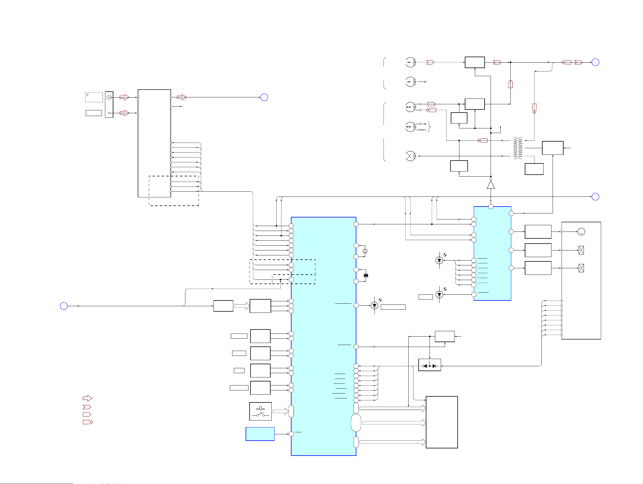
6-2. BLOCK DIAGRAM – TUNER/TAPE/PANEL Section –
FM/AM TUNER PACK
(Page 22)
MIC, SPEANA
H
FM 75Ω
(COAXIAL)
AM LOOP
FM ANT
AM ANT
• R-ch is omitted due to same as L-ch.
• SIGNAL PATH
: TUNER
: TAPE PLAY (DECK-A)
: TAPE PLAY (DECK-B)
: TAPE REC
TUNED
STEREO
MUTE
RDS DATA
RDS INT
FM-SOUT
(AEP, UK)
L-CH
R-CH
DO
R-CH
DATA
DI
CL
CE
IFC
CLK
PLL-CE
TUNED
STEREO
TU-MUTE
RDS-DATA
RDS-CLK
RDS-SIG
MIC
SPEANA
(AEP, UK)
AMP
Q201, 202
VOLUME
TREBLE
BASS
MULTI JOG
S301 – 323
(FRONT PANEL KEY)
TU
E
DATA
IFC
CLK
PLL-CE
TUNED
STEREO
TU-MUTE
RDS-DATA
RDS-CLK
RDS-SIG
BAND-PASS
FILTER
Q204 – 206
ROTARY
ENCODER
S801
ROTARY
ENCODER
S803
ROTARY
ENCODER
S802
ROTARY
ENCODER
S804
REMOTE CONTROL
RECEIVER
IC801
(Page 22)
DATA
CLK
3 TU/EVOL DO
96 TU DI
88 CLK
9 TU CE
75 TUNED
76 STEREO
85 TU MUTE
2 RDS DO
28 RDS CKL
19 TU-SIG/MIC
(EXCEPT US, Canadian, CIS)
21 SPEANA-L
22 SPEANA-M
23 SPEANA-H
77 VOL A
78 VOL B
81 TRE A
82 TRE B
83 BASS A
84 BASS B
79 JOG A
80 JOG B
KEY1 –
KEY3
26 – 24
29 RMC
SYSTEM CONTROLLER
IC901 (2/2)
A PHOTO/S6
B PHOTO/S7
A MODE/S13
REC FWD/S11
REC REV/S8
LCK
XT1
CF1
CF2
KEYSCAN
A HALF/S12
B HALF/S10
B MODE/S9
S14 – S25
S1 – S5,
S26 – S30
G1 – G11
8
1312XT2
15
16
93POWER LED
92
47
48
54
52
55
50
53
49
56-6730-40
41-45,
68-71,73
HP1
(PB)
(DECK-A)
HRPE1
(REC/PB/ERASE)
(DECK-B)
X901
32.768kHz
X902
8.64MHz
1 STANDBY/ON
S6
S7
S12
S10
S13
S9
S11
S8
L-CH
R-CH R-CH
L-CH
R-CH R-CH
ERASE
CLK
DATA
LED202 – 207
(ILLUMINATION)
LED901
B+
LED201
i-BASS
D620 – 627
S6 – S13
LCK
S-OUT
B+ SWITCH
B+
FL901
FLUORESCENT
INDICATOR TUBE
Q607
MUTING
Q305
MUTING
Q307, 309
PB SWITCH
Q301
PB SWITCH
Q303
18
SO
5 LCK
3 DATA
4 CLK
12 LED L3
13 LED L2
14 LED L1
15 LED R3
16 LED R2
17 LED R1
11 V-BASS
MOTOR/PLUNGER DRIVE,
+3.3V
Q601
6
PB2
O-MOTOR
LED DRIVE
IC201
R-CH
O-BIAS
SOL A
SOL B
BIAS OSC
L311
7
8
9
10
PB
REC
BIAS OSC
Q310
CAPSTAN/REEL
MOTOR DRIVE
Q601, 604
PLUNGER DRIVE
(DECK-A)
Q602, 605
PLUNGER DRIVE
(DECK-B)
Q603, 606
REC BIAS
SWITCH
Q311, 312
S6
S7
S12
S10
S13
S9
S11
S8
B+
(CD-VM)
DATA, CLK,
S-OUT, LCK
TAPE MECHANISM
DECK BLOCK
CAPM+
MM
(CAPSTAN/REEL)
A-SOL
(DECK-A)
B-SOL
(DECK-B)
A-PHOTO
B-PHOTO
A-HALF
B-HALF
A-MODE
B-MODE
REC (FWD)
REC (REV)
PB,
REC
CX-JN5
Ver 1.1
(Page 22)
F
(Page 22)
G
2121

CX-JN5
Ver 1.1
6-3. BLOCK DIAGRAM – AMP/POWER SUPPLY Section –
(Page 20)
(Page 21)
(Page 21)
(Page 20)
(Page 21)
(Page 21)
J401
MIC
J602
VIDEO/AUX
A
E
F
D
G
C
L
R
CD
TU
PB, REC PB
LM-L, LM-R,
TM-L, TM-R
DATA, CLK,
S-OUT, LCK
RESET,
P-DOWN
MIC LEVEL
AGC
Q401
MIC AMP
IC401 (1/2)
R-CH
MIC MIXING
REC
(E, E51, MX, SP, TW, KR, AUS)
VR401
MIC AMP
IC401 (2/2)
A-IN
19
B-IN
21
C-IN
23
PB1P
2
REC1O
28
PB-OUT
• R-ch is omitted due to same as L-ch.
• SIGNAL PATH
: CD
: TUNER
: TAPE PLAY (DECK-A)
: TAPE REC
: AUX IN
: MIC
RESET
P-DOWN
RESET SWITCH
Q901
MIC
D402
CONT
13
DATA
SPEANA
+
INPUT SELECT,
ELECTRICAL VOLUME
7
IC601
DBFB CONTROL
VOL-IN
• Abbreviation
AUS : Australian model
CND : Canadian model
E51 : Chilean and Peruvian models
KR : Korean model
MX : Mexican model
SP : Singapore model
TW : Taiwan model
RESET SIGNAL
GENERATOR
IC502
+3.3V
MIC, SPEANA
R-CH
Q641
17
BASS
LM-L
LM-R
TM-L
TM-R
OUT
D504
(Page 21)
H
FEED BACK
SWITCH
Q643
BASS BOOST ENHANCER
1
18
INA
BOOST
CONTROL
Q674 – 677
8 – 11 5 – 7
BOOST1 –
BOOST4
LM-L
14
LM-R
15
TM-L
12
TM-R
13
+4V
REGULATOR
IC501
V-STBY
IC671
OUTA6
GIN14VREF7BBE
13
FREQUENCY
Q671 – 673
BBE CONTROL,
LOADING/TABLE
MOTOR DRIVE
IC672
(AEP, UK, CIS, E51, MX)
+1.8V (MP3)
6
CONTROL
FREQ1 –
FREQ3
D091, 092
16
DATA3CLK
2
4
LCK
CLK
S-OUT
+1.8V
REGULATOR
IC803
+3.3V (CD)
POWER TRANSFORMER
PT011 (EXCEPT E, E51, SP, TW)
RECT
MUTING
Q181
R-CH
MUTING
CONTROL
Q183
BBE
LCK
MUTE
D697
+4V
PT002 (E, E51, SP, TW)
REGULATOR
VCC
(SUB)
OVER CURRENT
+4V
IC003
B+ SWITCH
Q023, 024
PRE DRIVE
Q101, 103
DETECT
Q281
CURRENT
MIRROR
Q105, 107
POWER
CASCADE
Q109, 111
TO
FLUORESCENT
INDICATOR TUBE
BIAS
Q117, 119
+6.4V (CD)
CD-VM
–VFL
R-CH
R-CH
+VP
FINAL DRIVE
Q121, 123
(AEP, UK, CIS)
Q125, 127
(EXCEPT AEP, UK, CIS)
VDD
VM
D691 – 694
VF1
VF2
SWITCHING
SWITCHING
–VP
R-CH
REGULATOR
REGULATOR
TO
POWER AMP
BLOCK
–32V
REGULATOR
Q041, 043, 044
Q231
Q232
+9V
IC002
+9V
IC001
VSS
OVER LOAD
DETECT
Q129
+
HOLD
Q282
+
+VH
–VH
+VL
–VL
R-CH
POWER
+VH
+VL
+VH
+VL
OUTPUT LEVEL
DETECT
Q233, 234
OUTPUT LEVEL
DETECT
Q235
+
THERMAL DETECT
+
DC DETECT
Q063, 064
AC DETECT
+
HOLD
Q045, 046
D067, 068
+
HOLD
POWER TRANSFORMER
PT003 (E, E51, SP, TW)
PT002 (EXCEPT E, E51, SP, TW)
RECT
D019 – 022
RECT
D009
RECT
D010
VM1
VM2
VH1
VH2
VL1
VL2
RELAY DRIVE
Q022
TH101, 102
Q291, 292
PROTECT
Q047
(MAIN)
R-CH
+
R-CH
(EXCEPT AEP, UK, CIS)
RELAY DRIVE
Q201
VH1, 2 (AC)
VH1, 2 (AC)
RY001
RY201
+
(E, E51, SP, TW)
S001
VOLTAGE SELECTOR
110 – 120V
220 – 240V
EXCEPT
E, E51, SP, TW
J221
PHONES
(AEP, UK, CIS)
J203
SPEAKER
+
L
–
+
R
–
M501
HOLD
(AC IN)
(FAN)
MM
B
FAN MOTOR
DRIVE
Q501, 503
(EXCEPT US, CND, AEP, UK, CIS)
MUTE, POWER,
(Page 20)
2222
CX-JN5
CD KEY board
SENSOR board
BD board
MOTOR (TB) board
DRIVER board
MOTOR (LD) board
SW board
KEY board
PT board
HEADPHONE board
PANEL board
MAIN board
TUNER PACK
Ver 1.1
6-4. NOTE FOR PRINTED WIRING BOARDS AND SCHEMATIC DIAGRAMS
Note on Printed Wiring Board:
• X : parts extracted from the component side.
• Y : parts extracted from the conductor side.
• x : parts mounted on the conductor side.
• : Pattern from the side which enables seeing.
(The other layers' patterns are not indicated.)
Caution:
Pattern face side: Parts on the pattern face side seen from
(Conductor Side) the pattern face are indicated.
Parts face side: Parts on the parts face side seen from
(Component Side) the parts face are indicated.
• Indication of transistor.
C
Q
B
E
B
These are omitted.
Q
CE
These are omitted.
Note on Schematic Diagram:
• All capacitors are in µF unless otherwise noted. pF: µµF
50 WV or less are not indicated except for electrolytics
and tantalums.
• All resistors are in Ω and 1/
specified.
f
•
• 2 : nonflammable resistor.
• 5 : fusible resistor.
• C : panel designation.
Note:
The components identified by mark 0 or dotted
line with mark 0 are critical for safety.
Replace only with part
number specified.
• A : B+ Line.
• B : B– Line.
•Voltages and waveforms are dc with respect to ground
•Voltages are taken with a V OM (Input impedance 10 MΩ).
•Waveforms are taken with a oscilloscope.
• Circled numbers refer to waveforms.
• Signal path.
•Abbreviation
: internal component.
under no-signal conditions.
– BD Section –
no mark : CD PLAY
– Other Sections –
no mark : FM
Voltage variations may be noted due to normal production tolerances.
Voltage variations may be noted due to normal production tolerances.
F : TUNER (FM/AM)
E : TAPE PLAY (DECK A)
d : TAPE PLAY (DECK B)
G : REC
J : CD PLAY
L : AUX IN
N : MIC INPUT
AUS: Australian model
CND : Canadian model
E51 : Chilean and Peluvian models
KR : Korean model
MX : Mexican model
SP : Singapore model
TW : T aiwan model
: Impossible to measure
∗
4
W or less unless otherwise
Note:
Les composants identifiés par
une marque 0 sont critiques
pour la sécurité.
Ne les remplacer que par une
pièce portant le numéro
spécifié.
• Circuit Boards Location
2323
CX-JN5
Ver 1.1
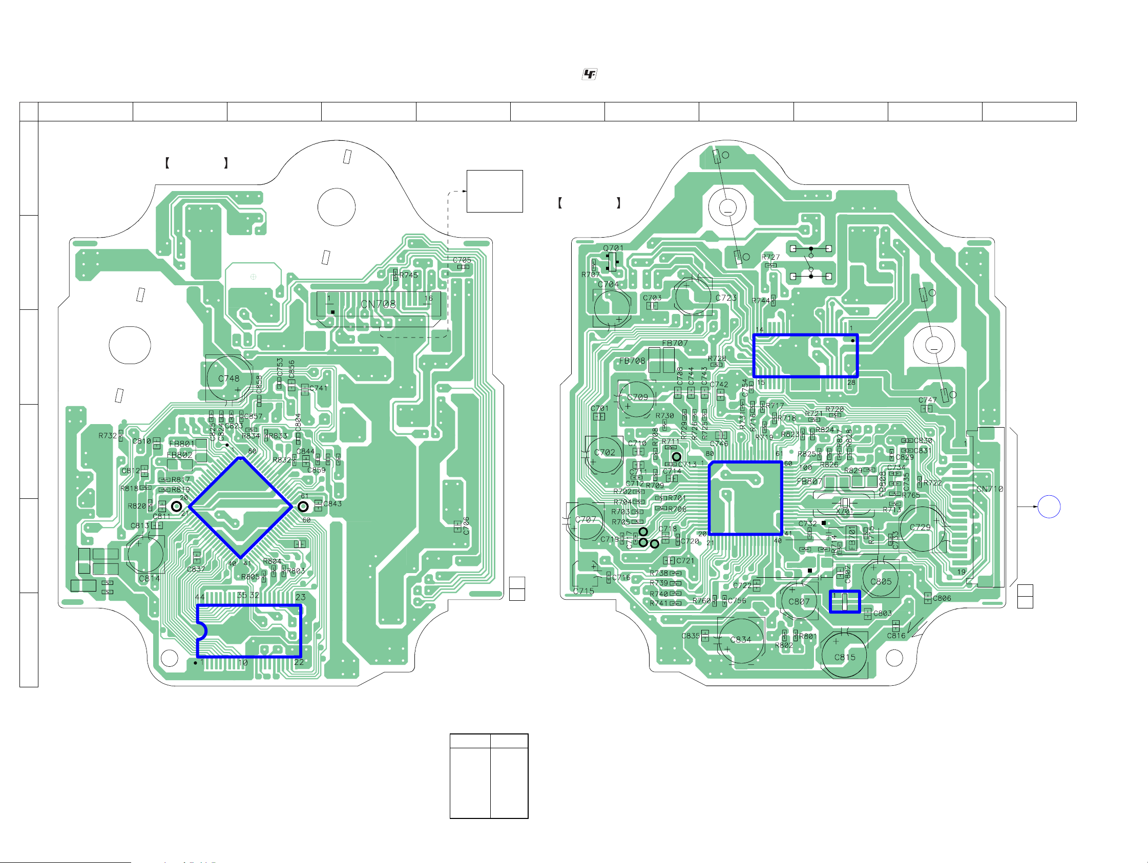
6-5. PRINTED WIRING BOARD – BD Section – (AEP, UK, CIS, E51, MX) • See page 23 for Circuit Boards Location. :Uses unleaded solder.
1 2 3 4 5 6 7 8 9 10 11
A
B
BD BOARD
(COMPONENT SIDE)
OPTICAL
PICK-UP
BLOCK
(KSM-213DCP)
BD BOARD
(CONDUCTOR SIDE)
B
C
E
+
M
M702
(SPINDLE)
–
S701
(LIMIT IN)
+
C
D
E
F
FB806
FB805
FB803
FB804
R806
R807
IC801
IC802
C817
C860
R860
1-688-077-
11
(11)
TP
(FE)
TP
(VC)
(TE)
M701
M
(SLED)
–
TP
(RF)
IC722
IC721
K
C902
TP
R747
R746
C901
5
34
1-688-077-
IC803
11
(11)
MAIN
BOARD
CN691
(Page 34)
• Semiconductor Location
Ref. No. Location
IC721 D-8
IC722 C-9
IC801 E-3
IC802 F-3
IC803 F-9
Q701 B-7
2424
 Loading...