

Sony CXG1108K Datasheet

Power Amplifier Module for JCDMA
Description
The CXG1108K is the power amplifier module
which operates at a single power supply. This IC is
designed using the Sony’s original p-Gate HFET
process.
Features
• Single power supply operation:
VDD1 = VDD2 = 3.5V,
VGG = 2.95V (@High mode),
VGG = 2.7V (@Low mode)
• Ultrasmall package: 0.065cc (6.2mm × 6.2mm × 1.7mm)
• High efficiency: ηadd = 37.5% (@900MHz, POUT = 27dBm)
• Output power (high/low mode switching supported):
POUT ≤ 17dBm: Low mode (VGG = 2.7V)
POUT = 17 to 27dBm: High mode (VGG 2.95V)
• Gain: Gp = 26dB (@900MHz)
CXG1108K
8 pin LCC (Ceramic)
Applications
Power amplifier for JCDMA system cellular phones
Structure
p-Gate HFET module
Recommended Operating Conditions
VDD = 3.3 to 4.2V
VGG = 2.95V±1% (High Mode)
2.7V±1% (Low Mode)
Absolute Maximum Ratings
• Operating case temperature Tcase –30 to +85 °C
• Storage temperature Tstg –30 to +125 °C
• Bias voltage VDD1, VDD2 6V
• Bias voltage VGG 3.3 V
(VDD1 = VDD2 = 3.5V)
• Input power PIN 8 dBm
GaAs module is ESD sensitive devices. Special handling precautions are required.
Sony reserves the right to change products and specifications without prior notice. This information does not convey any license by
any implication or otherwise under any patents or other right. Application circuits shown, if any, are typical examples illustrating the
operation of the devices. Sony cannot assume responsibility for any problems arising out of the use of these circuits.
– 1 –
E00Y33A25-PS
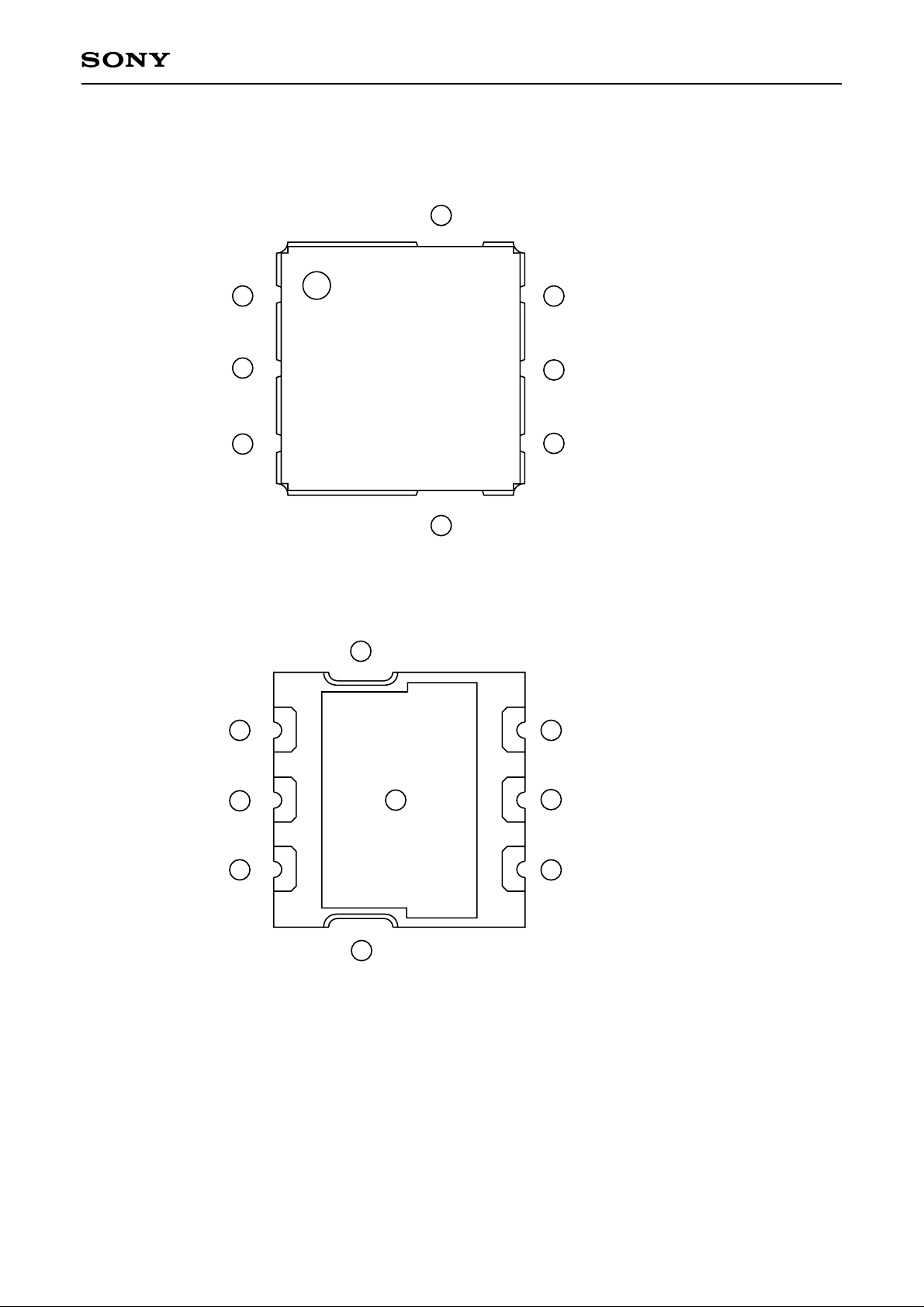
package Outline/Pin Configuration
Front
CXG1108K
7
GND
Back
1
P
IN
V
V
2
DD1
3
DD2
8
GND
7
GND
6
V
GG
6
V
GG
5
GND
4
P
OUT
1
P
IN
GND
P
OUT
5
9
GND
4
8
GND
2
DD1
V
3
V
DD2
– 2 –
 Loading...