

Sony CXG1091TN Datasheet
SP4T GSM Dualband Antenna Switch 5V + Logic
Description
The SP4T + logic is a high power antenna switch
MMIC for use in dualband GSM handsets.
One Antenna can be routed to either of the 2 Tx or
2 Rx ports. It operates from 3 CMOS control lines (Tx
ON/OFF and GSM900/1800 and Standby).
The Sony's J-FET process is used for low insertion
loss.
Features
• 3 CMOS compatible control lines
• 34dBm power handling at 5.0V (GSM900)
• Low second harmonic < – 30dBm at 34dBm
• Small package size: 16-pin TSSOP (3.9 × 4.1mm)
Applications
Dualband handsets using combinations of GSM900/GSM1800/GSM1900 and DECT
Structure
GaAs J-FET MMIC
Truth Table
– 1 –
E99758A9Y-PS
Sony reserves the right to change products and specifications without prior notice. This information does not convey any license by
any implication or otherwise under any patents or other right. Application circuits shown, if any, are typical examples illustrating the
operation of the devices. Sony cannot assume responsibility for any problems arising out of the use of these circuits.
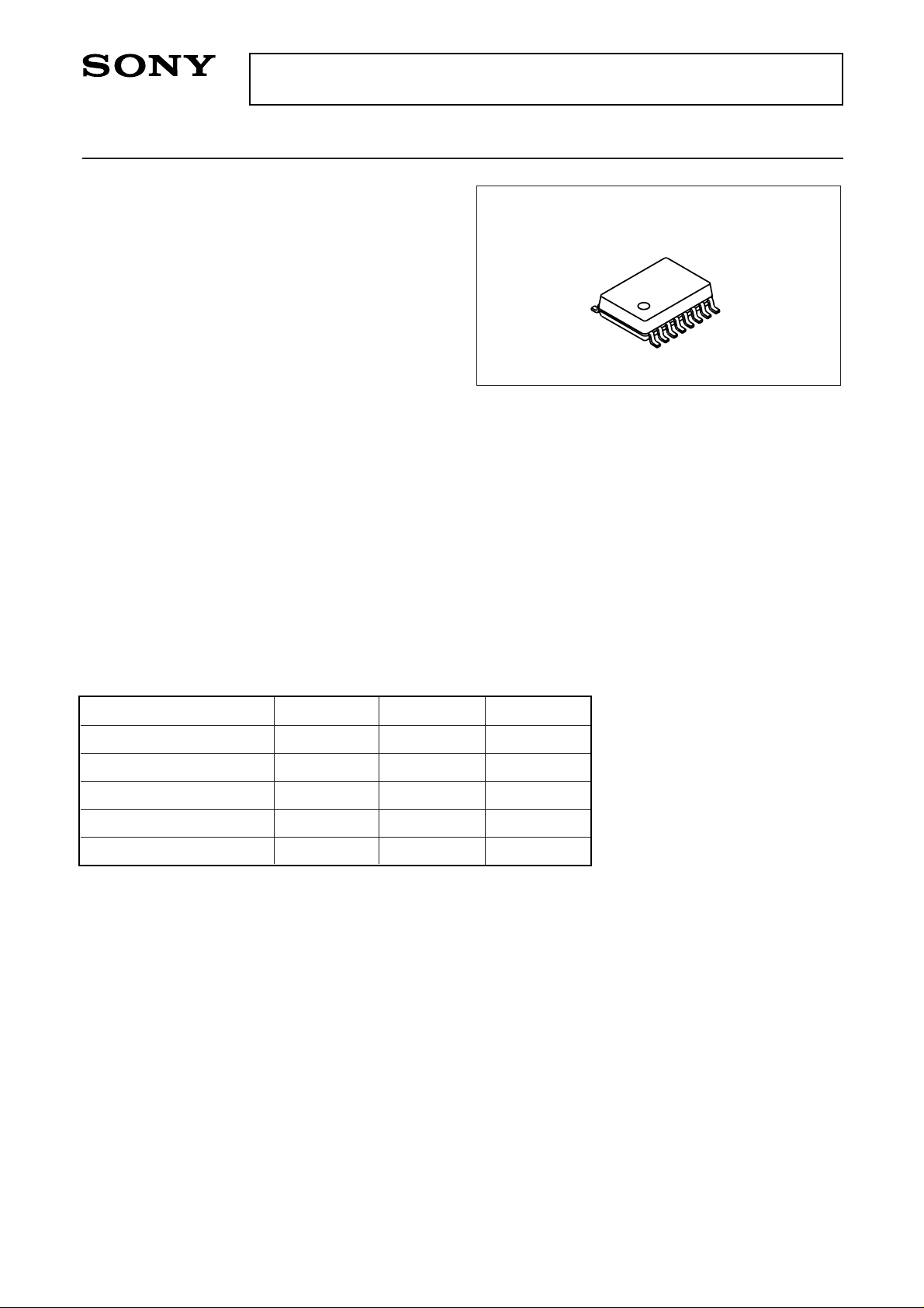
CXG1091TN
16 pin TSSOP (Plastic)
Absolute Maximum Ratings (Ta = 25°C)
• Bias voltage VDD 7V
•Control voltage Vctl 5 V
• Operating temperature Topr –35 to +85 °C
• Storage temperature Tstg –65 to +150 °C
GaAs MMICs are ESD sensitive devices. Special handling precautions are required.
On Pass
Ant.-Tx1 GSM900
Ant.-Tx2 GSM1800
Ant.-Rx1 GSM900/1800
Ant.-Rx2 GSM900/1800
OFF
Band select
H
L
L
H
—
Tx (H)/Rx (L)
H
H
L
L
—
Standby
H
H
H
H
L
For the availability of this product, please contact the sales office.
– 2 –
CXG1091TN
Electrical Characteristics (Ta = 25°C)
∗1
Pin = 34dBm, 880 to 915MHz, VDD = 5.0V
∗2
Pin = 32dBm, 1710 to 1785MHz, VDD = 5.0V
∗3
Pin = 10dBm, 925 to 960MHz
∗4
Pin = 10dBm, 1805 to 1880MHz
Note) Harmonics measured with Tx inputs harmonically matched.
CMOS Logic Values (Ta = 25°C)
Logic
High
Low
Min.
2.4V
Typ.
3.0V
0.0V
Max.
0.8V
Item
Insertion loss
Isolation
VSWR
Harmonics
Note)
P1dB compression input power
Switching speed
Control current
Supply current
Leakage current
IL
ISO.
VSWR
2fo
3fo
P1dB
TSW
ICTL
IDD
IIK
Port
Ant-Tx1, Tx2
Ant-Rx1, Rx2
Ant-Tx1, Tx2
Ant-Rx1, Rx2
Ant-Tx1, Tx2
Ant-Tx1, Tx2
Condition
∗1
∗2
∗3
∗4
∗1
∗2
∗3
∗4
∗1, ∗2
∗1, ∗2
∗1, ∗2
STBY = H
STBY = L
Min.
20
17
24
20
Typ.
0.5
0.6
0.55
0.7
25
20
28
24
1.2
36
1
100
0.5
Max.
0.75
0.85
0.75
0.9
–30
–30
1
50
Unit
dB
dB
dB
dB
dB
dB
dB
dB
dBm
dBm
dBm
µs
µA
mA
µA
Symbol
 Loading...