

Sony CXG1090TN Datasheet

CXG1090TN
High Power 2 ×4 Antenna Switch MMIC with Integrated Control Logic
Description
The CXG1090TN is a high power antenna switch
MMIC. The CXG1090TN is suited to connect Tx/Rx
to one of 4 antennas in cellular handset such as PDC.
The CXG1090TN has the integrated control logic
and can be operated with CMOS input.
This IC is designed using the Sony's GaAs J-FET
process which enable the CXG1090TN to be operated
with low voltage.
Features
• Low insertion loss: 0.30dB (Typ.)@900MHz, 0.40dB (Typ.)@1.5GHz
• Small package: TSSOP-16pin
• High power handling: PldB: 37dBm
• CMOS compatible input control
• Low bias voltage: VDD = 3.0V
Applications
2 × 4 antenna switch for digital cellular telephones such as PDC handsets.
Structure
GaAs J-FET MMIC
Absolute Maximum Ratings
• Bias voltage VDD 7 V @Ta = 25°C
• Control voltage Vctl 5 V @Ta = 25°C
• Operating temperature Topr –35 to +85 °C
• Storage temperature Tstg –65 to +150 °C
GaAs MMICs are ESD sensitive devices. Special handling precautions are required.
– 1 –
E99747A9Z-PS
Sony reserves the right to change products and specifications without prior notice. This information does not convey any license by
any implication or otherwise under any patents or other right. Application circuits shown, if any, are typical examples illustrating the
operation of the devices. Sony cannot assume responsibility for any problems arising out of the use of these circuits.
16 pin TSSOP (Plastic)
– 2 –
CXG1090TN
Block Diagram
RF5
(Rx)
RF4
(Ant/Ext.1)
RF6
(Diversity 1)
RF2
(Ant/Ext.2)
RF3
(Tx)
RF1
(Diversity 2)
RF-GND6 RF-GND1
F1
F3
F6F5
F7 F8
F2 F4
4
6
8
9
11
13
14
3
Package Outline/Pin Configuration
1
2
3
4
5
6
7
8
9
10
11
12
13
14
15
16
RF4
GND
RF5
GND
RF6
RF-GND6
V
DD
CTLA
RF3
GND
RF2
GND
RF1
RF-GND1
CTLC
CTLB
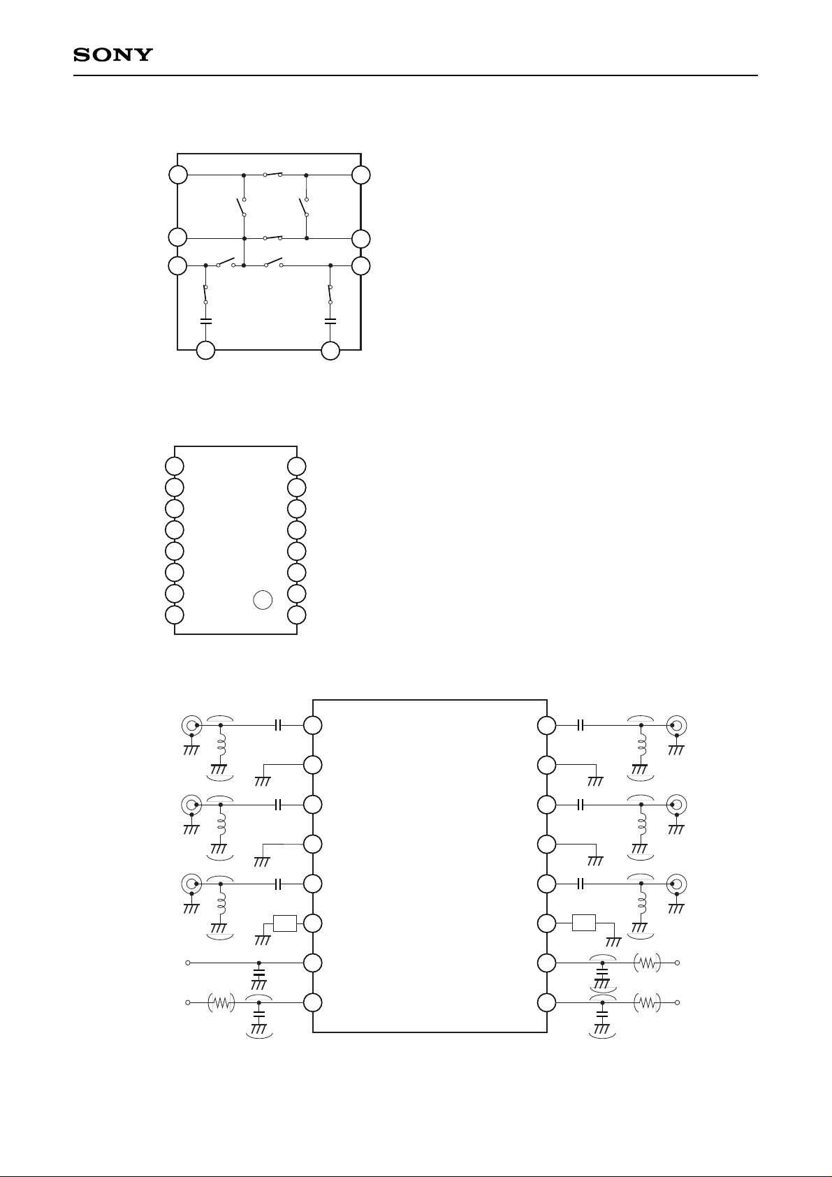
Recommended Circuit
1
2
3
4
5
6
7
8
9
10
11
12
13
14
15
16
RF3
GND
GND
RF-GND1
CTLC
CTLB
100pF
RF2
RF4
VDD
CTLA
RF5
GND
GND
RF-GND6
RF6
100pF
100pF
100pF
L1 L1
L1
L1
100pF
100pF
100pF
100pF
1kΩ
1kΩ
RF1
L1
L1
Z6
Z1
100pF
1kΩ
100pF
 Loading...