

Sony CXG1061TN Datasheet
—1—
E98335A8Y
Sony reserves the right to change products and specifications without prior notice. This information does not convey any license by
any implication or otherwise under any patents or other right. Application circuits shown, if any, are typical examples illustrating the
operation of the devices. Sony cannot assume responsibility for any problems arising out of the use of these circuits.
Absolute Maximum Ratings (Ta=25 °C)
• Supply voltage VDD 4.5 V
• Input power PIN +5 dBm
• Operating temperature Topr –35 to +85 °C
• Storage temperature Tstg –65 to +150 °C
Recommended Operating condition
• Supply voltage VDD 2.7 to 3.3 V
Description
The CXG1061TN is a low noise down conversion
mixer MMIC for PHS. This IC is designed using the
Sony’s GaAs J-FET process.
Features
• High gain Gc=22 dB (Typ.)
• Low distortion Input IP3=–13 dBm (Typ.)
• Low LO input power operation
PLO=–15 dBm
• High image suppression ratio
IMR=27 dBc (Typ.)
• LO input matching circuit
• Single 3 V power supply operation
• 10-pin TSSOP package
Function
Frequency conversion
Applications
Japan digital cordless telephones (PHS)
Structure
GaAs J-FET MMIC
Low Noise Down Conversion Mixer for PHS
10 pin TSSOP (Plastic)
CXG1061TN
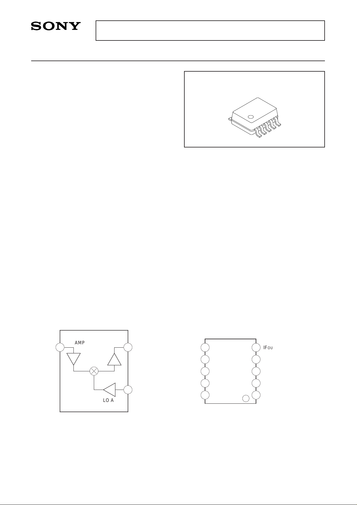
Block Diagram Pin Configuration
RFIN IFOUT
IF AMP
MIX
LO AMP
LO
IN
1
57
RF AMP
IFOUT/VDD (MIX, IF AMP)
CAP
GND
CAP
LO
IN
1
2
3
4
5
10
9
8
7
6
RFIN
CAP
GND
V
DD (LO AMP)
V
DD (RF AMP)
—2—
CXG1061TN
Electrical Characteristics
VDD=3.0 V, fRF=1.9 GHz, fLO=1.66 GHz, PLO=–15 dBm, RF input and IF output 50 Ω matching; unless otherwise specified
(Ta=25 °C)
Item
Current consumption
Conversion gain
Noise figure
Input IP3
Image suppression ratio
1/2 IF suppression ratio
LO to RF leak level
LO input VSWR
Symbol
IDD
Gc
NF
IIP3
IMR
1/2IFR
PLK
VSWRLO
Min.
—
19.5
—
–15.5
22
35
—
—
Typ.
7
22
3.3
–13
27
40
–46
2
Max.
9
24.5
4.5
—
—
—
–41
3.5
Unit
mA
dB
dB
dBm
dBc
dBc
dBm
—
Measurement condition
When no signal
When a small signal
When a small signal
PRF=–40 dBm
offset=600 kHz
Conversion by the IM3 suppression
ratio for two-wave input
When PRF=–40 dBm input
When PRF=–40 dBm input
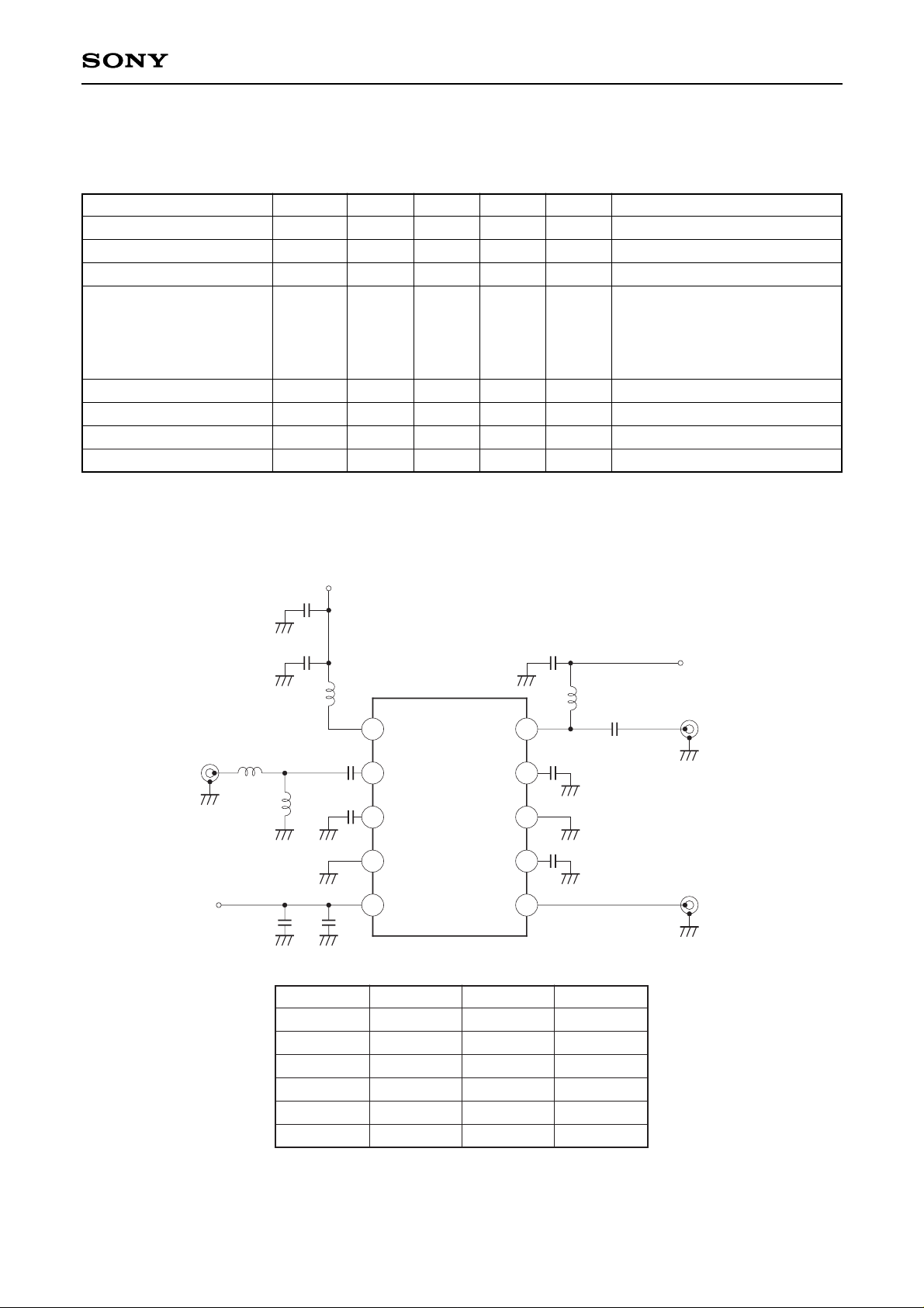
Recommended Evaluation Board
L1
C4
C6
C3
LOIN
50Ω
RFIN
50Ω
C1C2
V
DD (LO AMP)
C5
V
DD (MIX, IF AMP)
1
2
3
5
4
VDD
RFIN
CAP
GND
V
DD
IFOUT
CAP
GND
CAP
LO
IN
C10
C9
L2
C7
C8
VDD (RF AMP)
6
7
8
9
10
L3
L4
IF
OUT
50Ω
L1
L2
L3
L4
C1
C2
C3
82 nH
3.9 nH
12 nH
10 nH
18 pF
1000 pF
18 pF
C4
C5
C6
C7
C8
C9
C10
5 pF
1000 pF
0.1 µF
13 pF
1000 pF
3 pF
1000 pF
(Note) The values shown above are the specified values on the Sony’s recommended evaluation board.
 Loading...