

Sony CXG1053FN Datasheet

Power Amplifier/Antenna Switch + Low Noise Amplifier/Down Conversion Mixer for PHS
Description
The CXG1053FN is an MMIC consisting of the
power amplifier, antenna switch, low noise amplifier
and down conversion mixer.
This IC is designed using the Sony's GaAs J-FET
process featuring a single positive power supply
operation.
Features
• Operates at a single positive power supply: VDD = 3V
• Small mold package: 26-pin HSOF
<Power amplifier/antenna switch transmitter block >
• Low current consumption: IDD = 150mA
(POUT = 20.2dBm, f = 1.9GHz)
• High power gain: Gp = 39dB Typ.
(POUT = 20.2dBm, f = 1.9GHz)
<Antenna switch receiver block/
low noise amplifier>
• Low current consumption: IDD = 2.5mA Typ.
(When no signal)
• Low noise: NF = 2.7dB Typ. (f = 1.9GHz)
<Down conversion mixer>
• High conversion gain: Gc = 9dB Typ. (f = 1.9GHz)
• Low distortion: Input IP3 = +1dBm Typ. (f = 1.9GHz)
Applications
Japan digital cordless telephones (PHS)
Structure
GaAs J-FET MMIC
Absolute Maximum Ratings
<Power amplifier block>
• Supply voltage VDD 6V
•Voltage between gate and source
VGSO 1.5 V
• Drain current IDD 550 mA
• Allowable power dissipation
PD 3W
<Switch block>
Control voltage VCTL 6V
<Front-end block>
• Supply voltage VDD 6V
•Input power PRF +10 dBm
<Common to each block>
• Channel temperature Tch 150 °C
• Operating temperature Topr –35 to +85 °C
• Storage temperature Tstg –65 to +150 °C
– 1 –
E99852-PS
Sony reserves the right to change products and specifications without prior notice. This information does not convey any license by
any implication or otherwise under any patents or other right. Application circuits shown, if any, are typical examples illustrating the
operation of the devices. Sony cannot assume responsibility for any problems arising out of the use of these circuits.
CXG1053FN
26 pin HSOF (Plastic)
Note on Handling
GaAs MMICs are ESD sensitive devices. Special handling precautions are required.

– 2 –
CXG1053FN
VGG1
VPCTL
VGG2
POUT
TX
VCTL1
ANT
GND
RFOUT/VDD (RF AMP)
GND
RFIN (MIX)
VDD (LO AMP)
LOIN
PIN
GND
VDD1
VDD2
VDD3
GND
RX
VCTL2
RFIN
CAP
GND
CAP
IFOUT/VDD (IF AMP)
1
2
3
4
5
6
7
8
9
10
11
12
1314
15
16
17
18
19
21
20
22
23
24
25
26
Pin Configuration
2.2nH
P
IN
18nH
1nF
1nF
V
DD1
18nH
1nF
30pF
V
DD2
56nH
1nF
8pF
100pF
1.8nH
10nF
V
DD3
V
CTL2
100pF
1kΩ
(V
GG1)
(P
OUT)
(T
X)
VPCTL
1pF
100pF
VGG2
IFOUT
30pF
100nF
1nF
3.9nH
2.7nH
(RF
IN)
(R
X)
ANT
RFIN
(MIX)
VDD
(LO AMP)
LOIN
VCTL1
30pF
30pF
100pF
2.2nH
RFOUT
VDD
(RF AMP)
3.9nH
1.5nH
1nF
1nF
18pF
100pF
1
2
3
4
5
6
7
8
9
10
11
12
13
14
15
16
17
18
19
21
20
22
23
24
25
26
VDD
(IF AMP)
Block Diagram and External Circuit
– 3 –
CXG1053FN
2. Power Amplifier Block + Antenna Switch Transmitter Block
These specifications are when the Sony's recommended evaluation board with the external circuit shown on
page 7 is used. Therefore, the power amplifier output pin (POUT) and the antenna switch transmission input pin
(Tx) are connected via an external circuit. The specifications of the power amplifier block are set including the
antenna switch transmitter block.
Unless otherwise specified: VDD = 3V, VPCTL = 2V, VCTL1 = 3V, VCTL2 = 0V, IDD = 150mA,
POUT = 20.2dBm, f = 1.9GHz, Ta = 25°C
Current consumption
Gate voltage adjustment value
Output power
Power gain
Adjacent channel leak power ratio
(600 ± 100KHz)
Adjacent channel leak power ratio
(900 ± 100KHz)
Occupied bandwidth
2nd-order harmonic level
3rd-order harmonic level
Item Symbol
0
20.2
36
Min.
150
0.25
39
–63
–70
250
Typ.
0.6
–55
–60
275
–25
–25
Max.
mA
V
dBm
dB
dBc
dBc
KHz
dBc
dBc
Unit
Measured with the ANT pin
Measured with the ANT pin
Measured with the ANT pin
Measured with the ANT pin
Measured with the ANT pin
Measured with the ANT pin
Measurement conditions
Electrical Characteristics
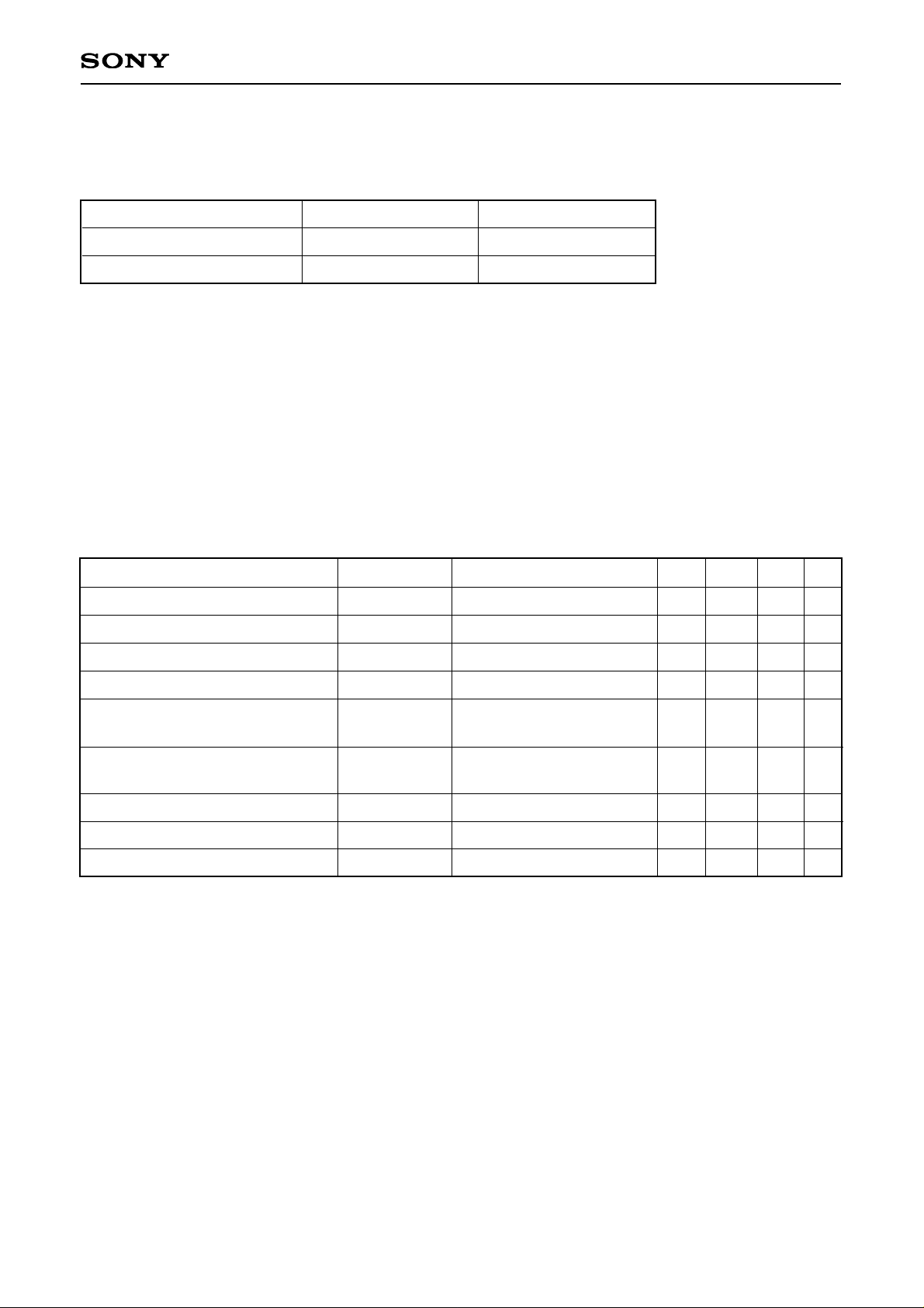
1. Control Pin Logic for Antenna Switch
Conditions of control pin ANT – TX ANT – RX
VCTL1 = 3V, VCTL2 = 0V
VCTL1 = 0V, VCTL2 = 3V
ON
OFF
OFF
ON
IDD
VGG
POUT
GP
ACPR600kHz
ACPR900kHz
OBW
—
—
 Loading...