

Sony CXG1047FN Datasheet
Dual-Band 3V Power Amplifier for GSM900/DCS1800 Applications
Description
The CXG1047FN dual band GaAs PA is a 3-stage
power amplifier that may be used for both GSM900
and DCS1800 applications. To achieve minimum
die-size and package dimensions, it contains one
amplifier chain with a single input and output.
The PA has a single RF input for both the GSM900
and DCS1800 transmit signals. The amplifier can be
configured for 2 separate inputs. Power control is
best achieved by variation of VDD1/VDD2 and VDD3
drain voltages with an external transistor. A proposed
power control circuit configuration is described.
External PMOS drain switch should be used to
achieve low leakage.
Features
• Single positive rail only
• Typical output power of 35.5dBm at 900MHz and 33dBm at 1800MHz
• Typical efficiency of 37% at 900MHz and 37% at 1800MHz
• Small package size with integral heat-sink: 16-pin HSOF (5.6 × 4.4 × 0.9mm)
• 3-stage amplifier chain
•Simple pin diode circuitry is used to switch between 1800 and 900MHz matching circuits
• Off mode insertion loss typically 27dB at 900MHz (Pin = +6dBm at VDD = 0V)
• Typical transmit noise @20MHz offset –79dBm/100kHz
Applications
Dual-band handsets transmitting on the GSM900 or DCS1800 frequencies
Structure
GaAs J-FET MMIC
Absolute Maximum Ratings (Ta = 25°C)
• Drain voltage VDD1, VDD2, VDD38 V
•Gate voltage VGG1, VGG2, VGG3 –5 to +1 V
• Input power Pin, max. 12 dBm
• Channel temperature Tch, max. 150 °C
• Operating temperature Ta –30 to +90 °C
• Storage temperature Tstg –40 to +150 °C
Note on Handling
GaAs MMICs are ESD sensitive devices. Special handling precautions are required. The IC will be damaged
in the range from 60 to 100V@200pF, 0Ω. The actual ESD test data will be submitted later.
– 1 –
E00223-PS
Sony reserves the right to change products and specifications without prior notice. This information does not convey any license by
any implication or otherwise under any patents or other right. Application circuits shown, if any, are typical examples illustrating the
operation of the devices. Sony cannot assume responsibility for any problems arising out of the use of these circuits.
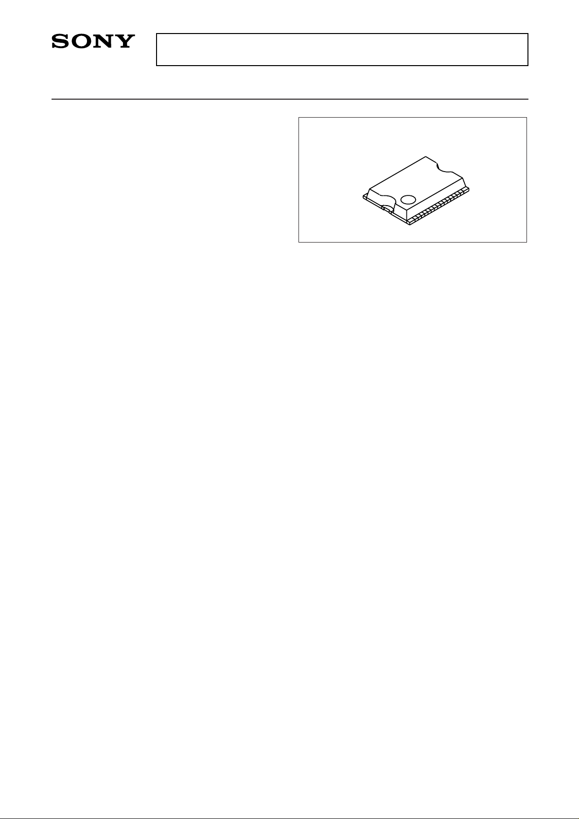
CXG1047FN
16 pin HSOF (Plastic)

– 2 –
CXG1047FN
Block Diagram
RFin
V
DD1 VDD2 VDD3
Antenna
Dual Band GSM900/18800 PA Configuration
Rx900/1800/(1900)
CXG1091/1092
Switched output
matching network
LPF
(> 2500MHz)
RF Out
DuplexerV
GG3VGG2VGG1
Pin Configuration
9
10
11
12
13
14
15
16
8
7
6
5
4
3
2
1
Vg1
RFin
NC
Vd1
NC
Vg2
Vd2
M900
GND
GND
Vd3/RFout
Vd3/RFout
Vd3/RFout
Vd3/RFout
NC
Vg3
Bottom GND
– 3 –
CXG1047FN
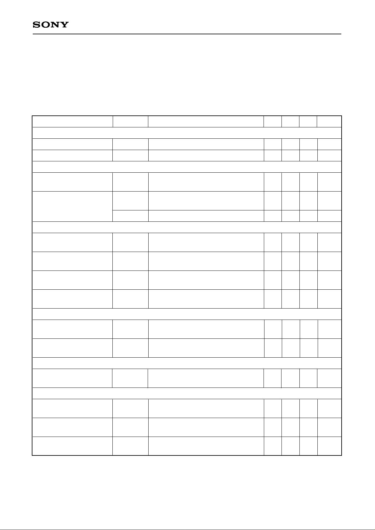
Power Amplifier Performance
Measurement Conditions: Ta = 25°C, Pin = +6dBm at 900MHz and Pin = +9dBm at 1750MHz,
pulsed DC conditions: 12.5% duty cycle 577µs burst duration.
All items are specified with the recommended schematic shown on page 6.
Item
Frequency
Frequency range (1)
Frequency range (2)
Output Power
(1) Output power –
900MHz
(2) Output power –
1750MHz
Power Control
Power control range
GSM900
Power control range
DCS1800
Off insertion loss –
900MHz
Off insertion loss –
1750MHz
Efficiency
Efficiency at 900MHz
Efficiency at 1750MHz
VSWR
Input VSWR at
GSM900/DCS1800
Harmonics Tx = 900MHz
2nd harmonics
3rd harmonics
4th harmonics
GSM900
DCS1800
POUT
POUT
POUT
PCTL
PCTL
Ins loss
Ins loss
PAE
PAE
VDD = 3.5V
VDD = 3.5V
VDD = 4V, Pin = +7dBm
∗1
∗1
VDD = 0V
Pin = +7dBm
VDD = 0V
Pin = +7dBm
VDD = 3.5V
Pin = +6dBm
VDD = 3.5V
Pin = +9dBm
After matching cct
Po = 35dBm@3.5V
After matching cct
Po = 35dBm@3.5V
After matching cct
Po = 35dBm@3.5V
880
1710
34.5
31.5
31.5
38
35
25
35
32
32
35.5
33
33
37
37
2:1
–30
–35
–40
915
1785
3:1
–25
–28
–33
MHz
MHz
dBm
dBm
dBm
dB
dB
dB
dB
%
%
dBc
dBc
dBc
Condition Min. Typ. Max. Unit
Symbol
 Loading...