

Sony CXG1028ATN Datasheet
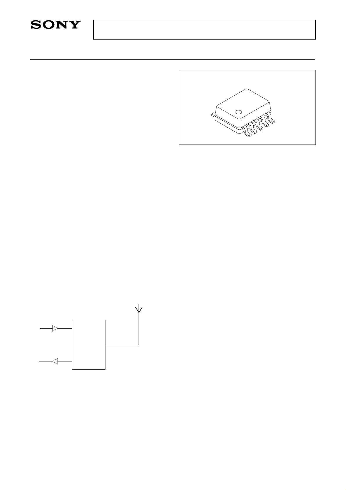
CXG1028ATN
10 pin TSSOP (Plastic)
E98527-PS
GSM900/1800/1900 SPDT TX/RX Switch
Description
The CXG1028ATN is a high power SPDT switch
suitable for Digital Cellular applications. This device
is part of a growing family of MMIC Antenna switches
for digital cellular and cordless radios. It uses the
state-of-the-art Sony GaAs JFET process.
Features
• Positive voltage supply only
• Low insertion loss, typically 0.3dB at
34.5dBm, 900MHz
• Low Harmonics: –64.5dBc Max. at 34.5dBm
(Vctl = 5V, 25°C)
• Stable Characteristics over wide temperature range
• Fast switching-100ns Typical
• Low current consumption, 190µA typical at 5V
• 10 pin TSSOP package (3.2 × 2.8mm)
Applications
• GSM900 handportable applications
• GSM1800 handportable
• GSM1900 handportable
• GSM900/1800/1900 Base station
• Other digital cellular and wireless local loop
applications
Typical Application
ESD
As with other GaAs semiconductors, ESD precautions
must be adhered to.
Sony reserves the right to change products and specifications without prior notice. This information does not convey any license by
any implication or otherwise under any patents or other right. Application circuits shown, if any, are typical examples illustrating the
operation of the devices. Sony cannot assume responsibility for any problems arising out of the use of these circuits.
TX IN
RX OUT
CXG1028ATN
PA
LNA
Internal
Antenna
– 1 –
– 2 –
CXG1028ATN
Electrical Characteristics
Measurement Conditions, unless otherwise stated:
Ta = 25°C. CW
Parameter
Insertion loss
Isolation
VSWR
Output Harmonics
Input Power for 0.2dB Compression
Input Power for 1dB Compression
Switching Speed TSW
Control Current
20
36
35
0.3
0.5
22
17
1.2
–35
36
35
38
37
100
190
0.6
0.8
–30
350
dB
dB
dB
dB
dBm
dBm
dBm
dBm
dBm
dBm
ns
µA
Min. Typ. Max. Unit
Control Voltage Selection, Vctl (H)
The choice of control voltage will determine the compression characteristic of the switch and the generation of
harmonics. The table above indicates P0.2dB, P1dB. The graphs below indicate the sensitivity of harmonic
levels:
2nd Harmonic with Power/Control Volts
–80
–70
–60
–50
–40
32 33 34 35 36
Input power [dBm]
Harmonic level [dBc]
Vctl = 0/3V
Vctl = 0/3.5V
Vctl = 0/4V
Vctl = 0/4.5V
Vctl = 0/5V
Condition
Symbol
∗1, ∗3
∗2, ∗4
∗1, ∗3
∗2, ∗4
∗1
∗2
∗1
∗2
∗1
∗2
IL
ISO
VSWR
2fo,3fo
P0.2dB
P1dB
TSW
ICTL
∗1
Pin = 34.5dBm, 880 to 915MHz, 0/5V Control
∗2
Pin = 32dBm, 1710 to 1785MHz, 0/5V Control
∗3
Pin = 10dBm, 925 to 960MHz, 0/3V Control
∗4
Pin = 10dBm, 1805 to 1880MHz, 0/3V Control
3rd Harmonic with Power/Control Volts
–90
–80
–70
–60
–50
–40
–30
–20
32 33 34 35 36
Input power [dBm]
Harmonic level [dBc]
Vctl = 0/3V
Vctl = 0/3.5V
Vctl = 0/4V
Vctl = 0/4.5V
Vctl = 0/5V
– 3 –
CXG1028ATN
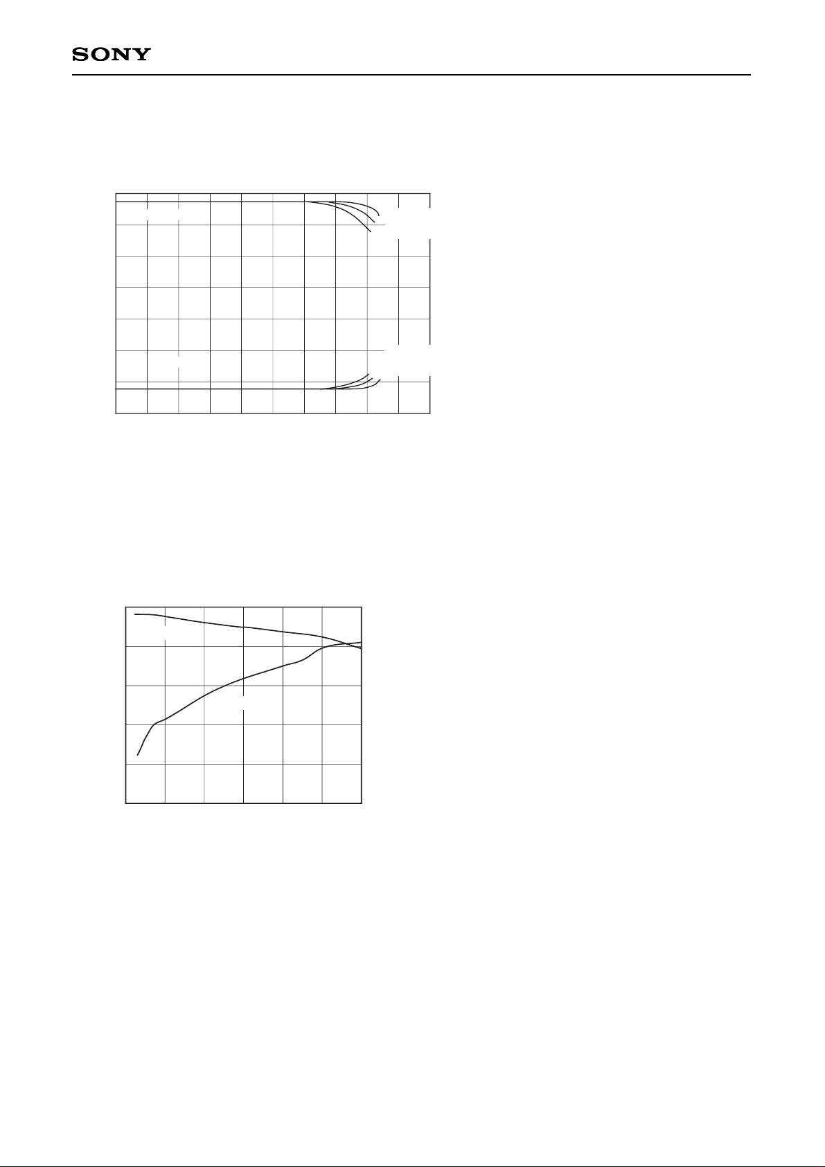
Compression Characteristics
Measurement Conditions: Vctl (L) = 0V, Ta = 25°C
0
–2
–4
–6
20 24 28 32 36 40
15
10
5
0
VCTL (H) = 5V
VCTL (H) = 4V
VCTL (H) = 3V
VCTL (H) = 3V
VCTL (H) = 4V
VCTL (H) = 5V
Input power (dBm)
Isolation (dB)
Insertion loss (dB)
Insertion loss, isolation vs. Input power
Insertion loss
Isolation
Frequency Characteristics
Measurement Conditions: Vctl (L) = 0V, Vctl (H) = 5V, Pin = 0dBm CW, Ta = 25°C
0
–3
–4
–5
–2
–1
–30
–20
–10
0
–40
–50
0 1 2 3
Insertion loss, isolation vs. Frequency
Frequency (GHz)
Isolation (dB)
Insertion loss (dB)
Isolation
Insertion loss
 Loading...