

Sony CXG1027TM Datasheet

Driver Amplifier for Transmission
Description
The CXG1027TM is a two-stage driver amplifier for
800 MHz and 1.5 GHz PDC. This is used to amplify
the transmission-side power of the RF signal.
Features
• Ultraminiature package (10 pin TSSOP)
• Low voltage operation
: 2.9 V (Min.)
• Low current consumption
: 45 mA (Typ.)
• High gain : 27.5 dB (Typ.) (for 1.5 GHz)
29.5 dB (Typ.) (for 800 MHz)
• Low distortion (Adjacent channel leak power ratio)
: –50 dBc (Typ.) (30 kHz offset)
–69 dBc (Typ.) (50 kHz offset)
• Positive power supply operation
(Adjustment-free for VGG)
• Supports both 800 MHz and 1.5 GHz by the
external matching circuit
CXG1027TM
10 pin TSSOP (Plastic)
Absolute Maximum Ratings (Ta=25 °C)
• Supply voltage VDD 6V
•Operating temperature
Topr –35 to +85 °C
• Storage temperature
Tstg –65 to +150 °C
• Allowable power dissipation
PD 550 mW
• Voltage between gate and source
VGSO 15 V
• Drain current 150 mA
Applications
Power amplification between the quadrature
modulator IC for 800 MHz/1.5 GHz PDC transmitter
(approx. –15 dBm output) and the power module or
power amplifier MMIC (approx. +10 dBm input)
Structure
GaAs MMIC
Operating Condition
Supply voltage VDD 3.4 V
VGG 0.2 V
Sony reserves the right to change products and specifications without prior notice. This information does not convey any license by
any implication or otherwise under any patents or other right. Application circuits shown, if any, are typical examples illustrating the
operation of the devices. Sony cannot assume responsibility for any problems arising out of the use of these circuits.
—1—
E97223-TE
CXG1027TM
Electrical Characteristics
VGG=0.2 V, VDD=3.4 V, f=941.5 MHz (Ta=25 °C)
Item
∗1
Current consumption
Output power
∗1Power gain
∗2Adjacent channel leak power ratio
(30 kHz offset)
∗2
Adjacent channel leak power ratio
(50 kHz offset)
Symbol
IDD
POUT
GP
ACPR30
ACPR50
Min.
10
27
Typ.
45
29.5
–50
–69
Max.
65
32
–47
–65
Unit
mA
dBm
dB
dBc
dBc
VGG=0.2 V, VDD=3.4 V, f=1.441 GHz (Ta=25 °C)
Item
∗1
Current consumption
Output power
∗1
Power gain
∗2
Adjacent channel leak power ratio
(30 kHz offset)
∗2
Adjacent channel leak power ratio
(50 kHz offset)
Symbol
IDD
POUT
GP
ACPR30
ACPR50
Min.
10
25
Typ.
45
27.5
–50
–69
Max.
65
30
–47
–65
Unit
mA
dBm
dB
dBc
dBc
∗1
: When +10 dBm output
∗2
: When +10 dBm output, 21 kHz band width
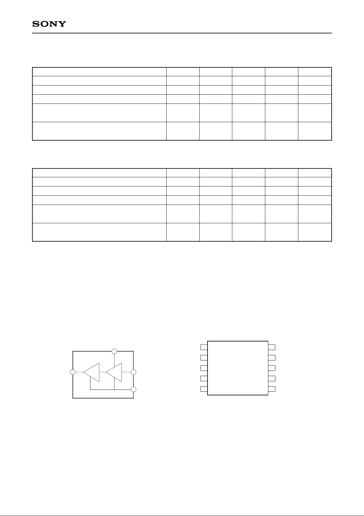
Block Diagram Package Description/Pin Configuration
VDD1
RFOUT/VDD2RFIN
VGG
GND (CAP)
OUT/VDD2
RF
110
GND
DD1
V
GND
10pin TSSOP (PLASTIC)
GND
GND (CAP)
RF
V
GND (1.5GHz) or
GND (IND) (800MHz)
IN
GG
—2—
 Loading...