

Sony CXD3005R Datasheet

CXD3005R
For the availability of this product, please contact the sales office.
CD Digital Signal Processor with Built-in Digital Servo and DAC
Description
The CXD3005R is a digital signal processor LSI for
CD players. This LSI incorporates a digital servo,
digital filter and 1-bit DAC.
Features
• All digital signal processing during playback is
performed with a single chip
• Highly integrated mounting possible due to a built-
in RAM
144 pin LQFP (Plastic)
Digital Signal Processor (DSP) Block
• Playback mode supporting CAV (Constant Angular
Velocity)
• Frame jitter free
• 0.5× to 20× continuous playback possible with a
low external clock
• Allows relative rotational velocity readout
• Wide capture range playback mode
• Spindle rotational velocity following method
• Supports 1× to 20× playback by switching the built-
in VCO
• The bit clock, which strobes the EFM signal, is
generated by the digital PLL
• EFM data demodulation
• Enhanced EFM frame sync signal protection
• Refined super strategy-based powerful error
correction
C1: double correction, C2: quadruple correction
Supported during 20× playback
• Noise reduction during track jumps
• Auto zero-cross mute
• Subcode demodulation and Sub Q data error
detection
• Digital spindle servo (built-in oversampling filter)
• 16-bit traverse counter
• Asymmetry compensation circuit
• CPU interface on serial bus
• Error correction monitor signal, etc. output from a
new CPU interface
• Servo auto sequencer
• Fine search performs track jumps with high
accuracy
• Digital audio interface outputs
• Digital level meter, peak meter
• Bilingual compatible
Digital Servo (DSSP) Block
• Microcomputer software-based flexible servo
control
• Offset cancel function for servo error signal
• Auto gain control function for servo loop
• E:F balance, focus bias adjustment function
• Surf jump function supporting micro two-axis
Digital Filter and DAC Blocks
• Digital de-emphasis
• Digital attenuation
• 4Fs oversampling filter
• Adoption of a secondary ∆∑ noise shaper
• Supports double-speed playback
Structure
Silicon gate CMOS IC
Absolute Maximum Ratings
• Supply voltage VDD –0.3 to +4.6 V
• Input voltage VI –0.3 to +4.6 V
(VSS – 0.3V to VDD + 0.3V)
• Output voltage VO –0.3 to +4.6 V
• Storage temperature Tstg –40 to +125 °C
• Supply voltage difference
VSS – AVSS –0.3 to +0.3 V
VDD – AVDD –0.3 to +0.3 V
Recommended Operating Conditions
• Supply voltage VDD
• Operating temperature
∗
The VDD (min.) for the CXD3005R varies
according to the playback speed and built-in VCO
selection. The VDD (min.) for the CXD3005R under
various conditions are as shown on the following
page.
∗
Topr –20 to +75 °C
3.0 to 4.0 V
Sony reserves the right to change products and specifications without prior notice. This information does not convey any license by
any implication or otherwise under any patents or other right. Application circuits shown, if any, are typical examples illustrating the
operation of the devices. Sony cannot assume responsibility for any problems arising out of the use of these circuits.
– 1 –
E97202A77
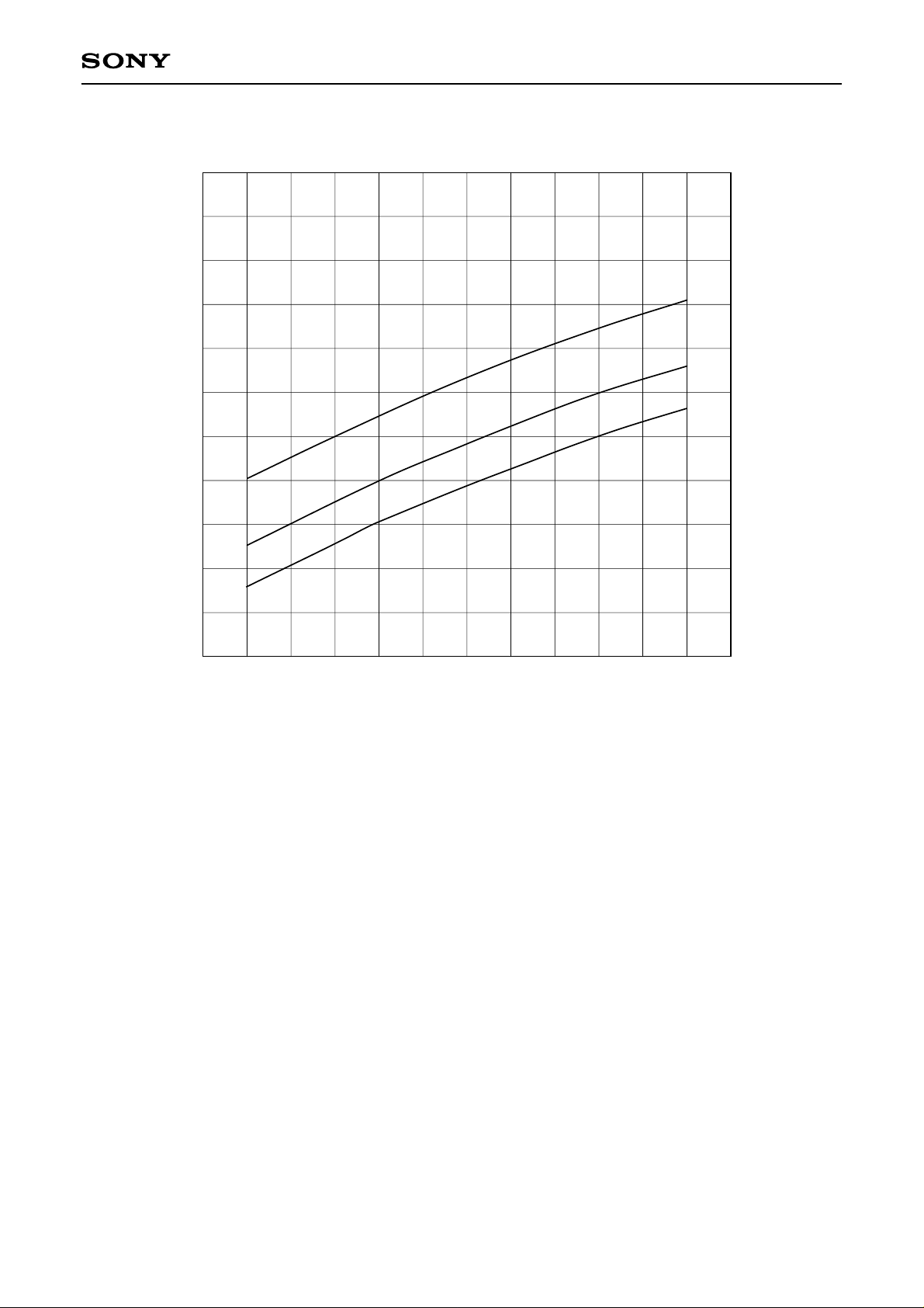
Maximum Operating Speed
24
23
CXD3005R
22
21
20
[Multiple]
19
18
17
16
15
3.0 3.1 3.2 3.3 3.4 3.5 3.6 3.7 3.8 3.9 4.0
[V]
+25°C
+55°C
+75°C
The maximum operating speed graph shows the playback speed VDD (min.) at various temperatures.
The playback conditions are middle-speed VCO1 and high-speed VCO2 selected in CAV-W mode with DSPB = 1.
– 2 –
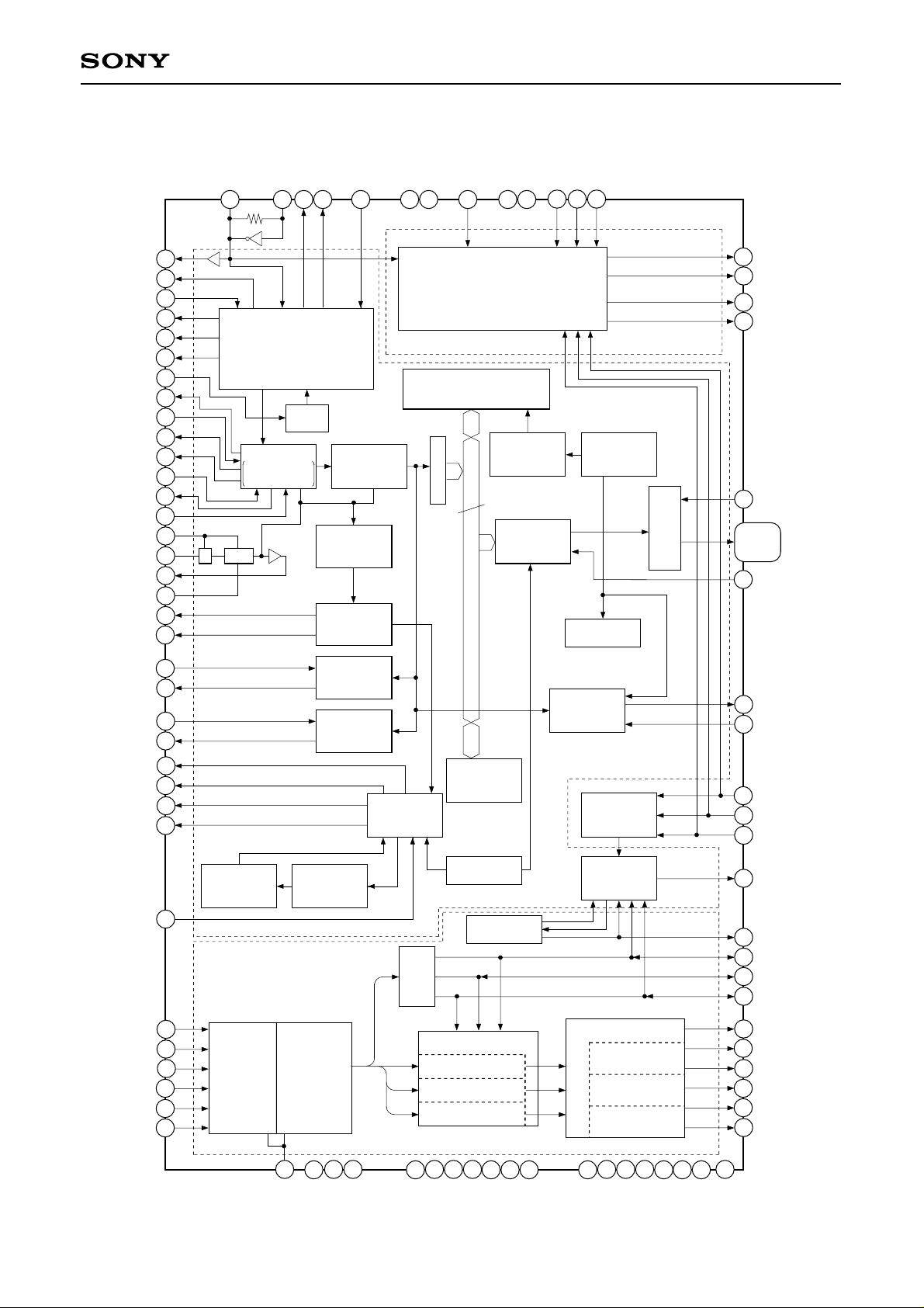
Block Diagram
CXD3005R
MCKO
V16M
VCKI
FSTO
C4M
C16M
VCTL
PDO
VCOI
VCOO
PCO
FILI
FILO
CLTV
RFAC
ASYI
ASYO
ASYE
WFCK
SCOR
EXCK
SBSO
SQCK
SQSO
MON
FSW
MDP
MDS
52
135
134
55
56
57
133
129
128
11
10
12
14
16
17
22
62
63
65
64
67
114
113
115
116
66
86
XTLO
87
XTLI
VPCO1
6
VPCO2
7
51
XTSL
75
DTS1
70
DTS2
77
XWO
78
DAS0
79
DAS1
PCMDI
28
30
BCKI
26
LRCKI
DAC Block
91
AO1F
4fs Digital Filter
+
1 bit DAC
92
83
82
AO1R
AO2F
AO2R
Clock
Generator
8
32K RAM
OSC
Digital PLL
Vari-Pitch
double speed
9
EFM
Demodulator
Register
Sync
∗
MUX
protector
Address
generator
8
D/A data
processor
Timing
Generator1
Priority
encoder
Peak
detector
processor
Serial/parallel
PSSL
23
49 to 44,
42 to 31,
29, 27
MUTE
61
DA01
to DA16
Subcode
P to W
processor
60
Subcode Q
Digital out
59
DOUT
MD2
processor
Error
CLV
processor
corrector
CPU interface
99
101
100
DATA
CLOK
XLAT
PWMI
RFDC
CE
TE
SE
FE
VC
112
140
141
142
Noise
Shaper
18-times
oversampling
Signal Processor Block
Servo Block
filter
MIRR
Generator 2
Servo
Interface
DFCT
FOK
SERVO DSP
Timing
OpAmp
3
AnaSw
A/D
CONVERTER
4
FOCUS SERVO
TRACKING SERVO
SLED SERVO
5
139
ADIO
130
131
TEST
132
TES2
TES3
0
DD
DV
20
1
DD
DV
18
1
DD
AV
136
2
DD
AV
3
DD
AV
4
DD
AV
5
DD
AV
Servo
auto
sequencer
PWM GENERATOR
FOCUS PWM
GENERATOR
TRACKING PWM
GENERATOR
SLED PWM
GENERATOR
13
138
21
2
1
SS
AV
SS
AV
3
SS
AV
0
SS
DV
1
SS
DV
4
SS
AV
5
SS
AV
69
XRST
95
103
104
105
106
120
121
122
123
124
125
SENS
COUT
MIRR
DFCT
FOK
SFDR
SRDR
TFDR
TRDR
FFDR
FRDR
– 3 –

Pin Configuration
CXD3005R
NC
NC
TESTA
PWMI
FSW
MON
MDP
MDS
LOCK
SSTP
DV
SS5
SFDR
SRDR
TFDR
TRDR
FFDR
FRDR
DV
DD5
NC
VCOO
VCOI
TEST
TES2
TES3
PDO
VCKI
V16M
AV
DD2
IGEN
AV
SS2
ADIO
RFDC
CE
TE
NC
NC
109
110
111
112
113
114
115
116
117
118
119
120
121
122
123
124
125
126
127
128
129
130
131
132
133
134
135
136
137
138
139
140
141
142
143
144
108
NC
107
NC
106
FOK
DFCT
104105
MIRR
103
COUT
102
4
SS
DV
101
CLOK
100
XLAT
99
DATA
98
ATSK
97
SCLK
96
DIRC
95
SENS
94
4
DD
DV
3
DD
AO1R
AV
93
92
91
AO1F
90
NC
3
5
SS
SS
AV
AV
89
88
5
4
DD
DD
AV
XTLI
XTLO
86
87
AO2F
AV
84
83
85
82
AO2R
81
4
SS
AV
3
SS
DAS1
DV
80
79
78
DAS0
XWO
7677
DTS0
75
DTS1
74
NC
NC
73
72
NC
71
NC
70
DTS2
69
XRST
68
SCSY
67
SQCK
66
SQSO
65
EXCK
64
SBSO
63
SCOR
62
WFCK
61
MUTE
60
DOUT
59
MD2
58
DD3
DV
57
C16M
56
C4M
55
FSTO
54
NC
53
FSTI
MCKO
52
51
XTSL
50
SS2
DV
DA01
49
48
DA02
47
DA03
46
DA04
45
DA05
44
DA06
43
DV
DD2
42
DA07
DA08
41
40
DA09
39
DA10
38
NC
37
NC
FILI
11
PCO
12
13
CLTV
1
SS
AV
14 15
RFAC
16
BIAS
6
NC
5
4
3
FE
SE
VC
1
2
NC
7
VPCO2
VPCO1
8
VCTL
9
10
FILO
17
ASYI
18
ASYO
1
DD
AV
19
20
NC
1
DD
DV
23
21
22
1
SS
ASYE
DV
24
PSSL
25
LRCK
WDCK
26
LRCKI
27 28
DA16
29
DA15
PCMDI
30
BCKI
313233
DA14
DA13
34
DA12
35
DA11
NC
36
NC
– 4 –
Pin Description
CXD3005R
Pin
No.
3
4
5
6
7
8
9
10
11
12
13
14
15
16
Symbol I/O Description
SE
FE
VC
VPCO1
VPCO2
VCTL
FILO
FILI
PCO
CLTV
AVSS1
RFAC
BIAS
ASYI
O
O
O
O
I
I
I
1, Z, 0
1, Z, 0
I
Analog
I
1, Z, 0
I
I
I
I
Sled error signal input.
Focus error signal input.
Center voltage input.
Wide-band EFM PLL VCO2 charge pump output.
Wide-band EFM PLL VCO2 charge pump output 2. Turned on and off by $E
command FCSW.
Wide-band EFM PLL VCO2 control voltage input.
Master PLL filter output (slave = digital PLL).
Master PLL filter input.
Master PLL charge pump output.
Multiplier VCO control voltage input.
Analog GND.
EFM signal input.
Asymmetry circuit constant current input.
Asymmetry comparator voltage input.
17
18
20
21
22
23
24
25
26
27
28
29
30
31
32
ASYO
AVDD1
DVDD1
DVSS1
ASYE
PSSL
WDCK
LRCK
LRCKI
DA16
PCMDI
DA15
BCKI
DA14
DA13
O
1, 0
EFM full-swing output (low = VSS, high = VDD).
Analog power supply.
Digital power supply.
Digital GND.
I
I
O
1, 0
O
1, 0
I
O
1, 0
I
O
1, 0
I
O
1, 0
O
1, 0
Asymmetry circuit on/off (low = off, high = on).
Audio data output mode switching input (low: serial, high: parallel).
D/A interface for 48-bit slot. Word clock f = 2Fs.
D/A interface for 48-bit slot. LR clock f = Fs.
LR clock input to DAC (48-bit slot).
DA16 (MSB) output when PSSL = 1, 48-bit slot serial data output (two's
complement, MSB first) when PSSL = 0.
Audio data input to DAC (48-bit slot).
DA15 output when PSSL = 1, 48-bit slot bit clock output when PSSL = 0.
Bit clock input to DAC (48-bit slot).
DA14 output when PSSL = 1, 64-bit slot serial data output (two's
complement, LSB first) when PSSL = 0.
DA13 output when PSSL = 1, 64-bit slot bit clock output when PSSL = 0.
33
34
39
40
DA12
DA11
DA10
DA09
O
1, 0
O
1, 0
O
1, 0
O
1, 0
DA12 output when PSSL = 1, 64-bit slot LR clock output when PSSL = 0.
DA11 output when PSSL = 1, GTOP output when PSSL = 0.
DA10 output when PSSL = 1, XUGF output when PSSL = 0.
DA09 output when PSSL = 1, XPLCK output when PSSL = 0.
– 5 –
CXD3005R
Pin
No.
41
42
43
44
45
46
47
48
49
50
51
52
53
55
56
Symbol I/O Description
O
DA08
DA07
DVDD2
DA06
DA05
DA04
DA03
DA02
DA01
DVSS2
XTSL
MCKO
FSTI
FSTO
C4M
1, 0
O
1, 0
DA08 output when PSSL = 1, GFS output when PSSL = 0.
DA07 output when PSSL = 1, RFCK output when PSSL = 0.
Digital power supply.
O
1, 0
O
1, 0
O
1, 0
O
1, 0
O
1, 0
O
1, 0
DA06 output when PSSL = 1, C2PO output when PSSL = 0.
DA05 output when PSSL = 1, XRAOF output when PSSL = 0.
DA04 output when PSSL = 1, MNT3 output when PSSL = 0.
DA03 output when PSSL = 1, MNT2 output when PSSL = 0.
DA02 output when PSSL = 1, MNT1 output when PSSL = 0.
DA01 output when PSSL = 1, MNT0 output when PSSL = 0.
Digital GND.
I
O
1, 0
I
O
1, 0
O
1, 0
Crystal selection input.
Clock output. Inverted output of XTLI.
2/3 frequency division input for XTLI pin.
2/3 frequency division output for XTLI pin. Does not change with variable pitch.
1/4 frequency division output for XTLI pin. Changes with variable pitch.
57
58
59
60
61
62
63
64
65
66
67
68
69
70
75
76
C16M
DVDD3
MD2
DOUT
MUTE
WFCK
SCOR
SBSO
EXCK
SQSO
SQCK
SCSY
XRST
DTS2
DTS1
DTS0
O
1, 0
16.9344MHz output. Changes simultaneously with variable pitch.
Digital power supply.
I
O
1, 0
I
O
1, 0
O
1, 0
O
1, 0
I
O
1, 0
I
I
I
I
I
I
Digital Out on/off control (low = off, high = on).
Digital Out output.
Mute (low: off, high: on).
WFCK (Write Frame Clock) output.
Outputs a high signal when either subcode sync S0 or S1 is detected.
Sub P to W serial output.
SBSO readout clock input.
Sub Q 80-bit and PCM peak and level data 16-bit output.
SQSO readout clock input.
GRSCOR re-synchronization input. Normally low, re-syncronization is
executed when high.
System reset. Reset when low.
DAC test pin. Normally fixed to high.
DAC test pin. Normally fixed to high.
DAC test pin. Normally fixed to low.
77
78
79
80
81
82
XWO
DAS0
DAS1
DVSS3
AVSS4
AO2R
I
I
I
DAC sync window open input. Normally high, window open when low.
DAC test pin. Normally fixed to high.
DAC test pin. Normally fixed to low.
Digital GND.
Analog GND.
O
1, Z, 0
Channel 2 DAC PWM output (reversed phase).
– 6 –
Pin
No.
CXD3005R
Symbol I/O Description
83
84
85
86
87
88
89
91
92
93
94
95
96
97
98
99
100
AO2F
AVDD4
AVDD5
XTLO
XTLI
AVSS5
AVSS3
AO1F
AO1R
AVDD3
AVDD4
SENS
DIRC
SCLK
ATSK
DATA
XLAT
O
1, Z, 0
Channel 2 DAC PWM output (forward phase).
Analog power supply.
Master clock power supply.
O
1, 0
I
Master clock crystal oscillation circuit output.
Master clock crystal oscillation circuit input.
Master clock GND.
Analog GND.
O
1, Z, 0
O
1, Z, 0
Channel 1 DAC PWM output (forward phase).
Channel 1 DAC PWM output (reversed phase).
Analog power supply.
Digital power supply.
O
1, Z, 0
I
I
I
I
I
SENS output to CPU.
Used during 1-track jumps.
SENS serial data readout clock input.
Anti-shock pin.
Serial data input from CPU.
Latch input from CPU. Serial data is latched at the falling edge.
101
102
103
104
105
106
111
112
113
114
115
116
117
118
119
CLOK
DVSS4
COUT
MIRR
DFCT
FOK
TESTA
PWMI
FSW
MON
MDP
MDS
LOCK
SSTP
DVSS5
I/O
I/O
I/O
I/O
O
O
O
O
I/O
I
I
I
1, 0
1, 0
1, 0
1, 0
1, Z, 0
1, 0
1, Z, 0
1, Z, 0
1, 0
Serial data transfer clock input from CPU.
Digital GND.
Track count signal I/O.
Mirror signal I/O.
Defect signal I/O.
Focus OK signal I/O.
Test pin. Leave this open.
Spindle motor external pin input.
Spindle motor output filter switching output.
GRSCOR output when $8 command SCOR SEL = high.
Spindle motor on/off control output.
Spindle motor servo control output.
Spindle motor servo control output.
GFS is sampled at 460Hz; when GFS is high, this pin outputs a high signal.
If GFS is low eight consecutive samples, this pin outputs low. Input when
LKIN = high.
Disc innermost track detection signal input.
Digital GND.
120
121
122
SFDR
SRDR
TFDR
O
1, 0
O
1, 0
O
1, 0
Sled drive output.
Sled drive output.
Tracking drive output.
– 7 –
Pin
No.
123
124
125
126
128
Symbol I/O Description
O
TRDR
FFDR
FRDR
DVDD5
VCOO
1, 0
O
1, 0
O
1, 0
Tracking drive output.
Focus drive output.
Focus drive output.
Digital power supply.
O
1, 0
Analog EFM PLL oscillation circuit output.
CXD3005R
VCOI
129
TEST
130
TES2
131
TES3
132
PDO
133
VCKI
134
V16M
135
AVDD2
136
IGEN
137
AVSS2
138
ADIO
139
RFDC
140
CE
141
TE
142
∗
In the CXD3005R, the following pins are NC.
I
I
I
I
O
1, Z, 0
I
O
1, Z, 0
Analog EFM PLL oscillation circuit input. flock = 8.6436MHz
Test pin. Normally fixed to low.
Test pin. Normally fixed to low.
Test pin. Normally fixed to low.
Analog EFM PLL charge pump output.
Variable pitch clock input from the external VCO. fcenter = 16.9344MHz
Set VCKI to low when the external clock is not input to this pin.
Wide-band EFM PLL VCO2 oscillation output.
Analog power supply.
I
Connects the operational amplifier current source reference resistance connection.
Analog GND.
O
I
I
I
Operational amplifier output.
RF signal input.
Center servo analog input.
Tracking error signal input.
Pins 1, 2, 19, 35, 36, 37, 38, 54, 71, 72, 73, 74, 90, 107, 108, 109, 110, 127, 143 and 144
Notes) • The 64-bit slot is an LSB first, two's complement output. The 48-bit slot is an MSB first, two's
complement output.
• GTOP is used to monitor the frame sync protection status. (High: sync protection window released.)
• XUGF is the frame sync obtained from the EFM signal, and is negative pulse. It is the signal before
sync protection.
• XPLCK is the inverse of the EFM PLL clock. The PLL is designed so that the falling edge and the
EFM signal transition point coincide.
• The GFS signal goes high when the frame sync and the insertion protection timing match.
• RFCK is derived from the crystal accuracy, and has a cycle of 136µs.
• C2PO represents the data error status.
• XRAOF is generated when the 32K RAM exceeds the ±28F jitter margin.
– 8 –
CXD3005R
Electrical Characteristics
1. DC Characteristics (VDD = AVDD = 3.3V ± 10%, VSS = AVSS = 0V, Topr = –20 to +75°C)
Input voltage (1)
Input voltage (2)
Input voltage (3)
Input voltage (4)
Input voltage (5)
Input voltage (6)
Output voltage (1)
Output voltage (2)
Output voltage (3)
Item
High level input voltage
Low level input voltage
High level input voltage
Low level input voltage
High level input voltage
Low level input voltage
High level input voltage
Low level input voltage
Input voltage
Input voltage
High level output voltage
Low level output voltage
High level output voltage
Low level output voltage
High level output voltage
Low level output voltage
VIH (1)
VIL (1)
VIH (2)
VIL (2)
VIH (3)
VIL (3)
VIH (4)
VIL (4)
VIN (5)
VIN (6)
VOH (1)
VOL (1)
VOH (2)
VOL (2)
VOH (3)
VOL (3)
Conditions Min. Typ. Max. Unit
0.7VDD
0.2VDD
0.7VDD
Schmitt input
0.2VDD
0.7VDD
VI ≤ 5.5V
0.2VDD
VI ≤ 5.5V
Schmitt input
Analog input
Analog input
IOH = –8mA
IOL = 8mA
IOH = –4mA
IOL = 4mA
IOH = –2mA
IOL = 4mA
0.7VDD
VSS
VSS
VDD – 0.4
0
VDD – 0.4
0
VDD – 0.2
0
0.2VDD
VDD
VDD
VDD
0.4
VDD
0.4
VDD
0.4
Applicable pins
V
∗1, ∗12
V
V
∗2
V
V
∗3
V
V
∗4
V
∗5
V
∗6
V
V
∗9
V
V
∗7, ∗10
∗12
V
V
∗7, ∗10
∗12
V
Output voltage (4)
Low level output voltage
High level output voltage
Output voltage (5)
Low level output voltage
Input leak current (1)
Input leak current (2)
Tri-state pin
output leak current
VOL (4)
VOH (5)
VOL (5)
ILI (1)
ILI (2)
ILO
IOL = 4mA
IOH = –0.28mA
IOH = 0.36mA
VI = 0 to 5.5V
VI = 0.25VDD
to 0.75VDD
VO = 0 to 3.6V
0
VDD – 0.5
0
–10
–20
–5
0.4
VDD
0.4
10
20
5
V
V
V
µA
µA
µA
∗8
∗11
∗3, ∗4, ∗5
∗6
∗10
Applicable pins
∗1
BCKI, DTS0, DTS1, DTS2, LRCKI, PCMDI, TES2, TES3, TEST
∗2
ASYE, FSTI, VCKI
∗3
ATSK, DATA, DIRC, MD2, PWMI, SSTP, XLAT, XTSL, XWO
∗4
CLOK, EXCK, MUTE, SCLK, SCSY, SQCK, XRST
∗5
ASYI, BIAS, CLTV, FILI, IGEN, RFAC, VCTL
∗6
CE, FE, SE, TE, VC, RFDC
∗7
ASYO, C16M, C4M, DA01 to DA16, DAS0, DAS1, DOUT, FFDR, FRDR, FSTO, LRCK, MON, PSSL,
SBSO, SCOR, SFDR, SQSO, SRDR, TFDR, TRDR, WDCK, WFCK
∗8
FSW
∗9
MCKO
∗10
AO1F, AO1R, AO2F, AO2R, MDP, MDS, PCO, PDO, SENS, V16M, VPCO1, VPCO2
∗11
FILO
∗12
COUT, DFCT, FOK, LOCK, MIRR
– 9 –
2. AC Characteristics
(1) XTLI pin, VCOI pin
(a) When using self-excited oscillation
(Topr = –20 to +75°C, VDD = AVDD = 3.3V ±10%)
CXD3005R
Item Symbol Min. Typ. Max.
Oscillation
frequency
fMAX 7
(b) When inputting pulses to XTLI and VCOI pins
(Topr = –20 to +75°C, VDD = AVDD = 3.3V ±10%)
Item Symbol Min. Typ. Max. Unit
High level pulse
width
Low level pulse
width
Pulse cycle
tWHX
tWLX
tCX
13 500
13 500
26 1000
Input high level VIHX VDD – 1.0
Input low level VILX 0.8
Rise time,
fall time
tR, tF
34
10
Unit
MHz
ns
ns
ns
V
V
ns
tCX
tWHX
XTLI
tR tF
tWLX
V
IHX
V
IHX × 0.9
V
DD/2
VIHX × 0.1
VILX
(c) When inputting sine waves to XTLI and VCOI pins via a capacitor
(Topr = –20 to +75°C, VDD = AVDD = 3.3V ±10%)
Item Symbol Min. Typ. Max. unit
Input amplitude VI 2.0 VDD + 0.3 Vp-p
– 10 –
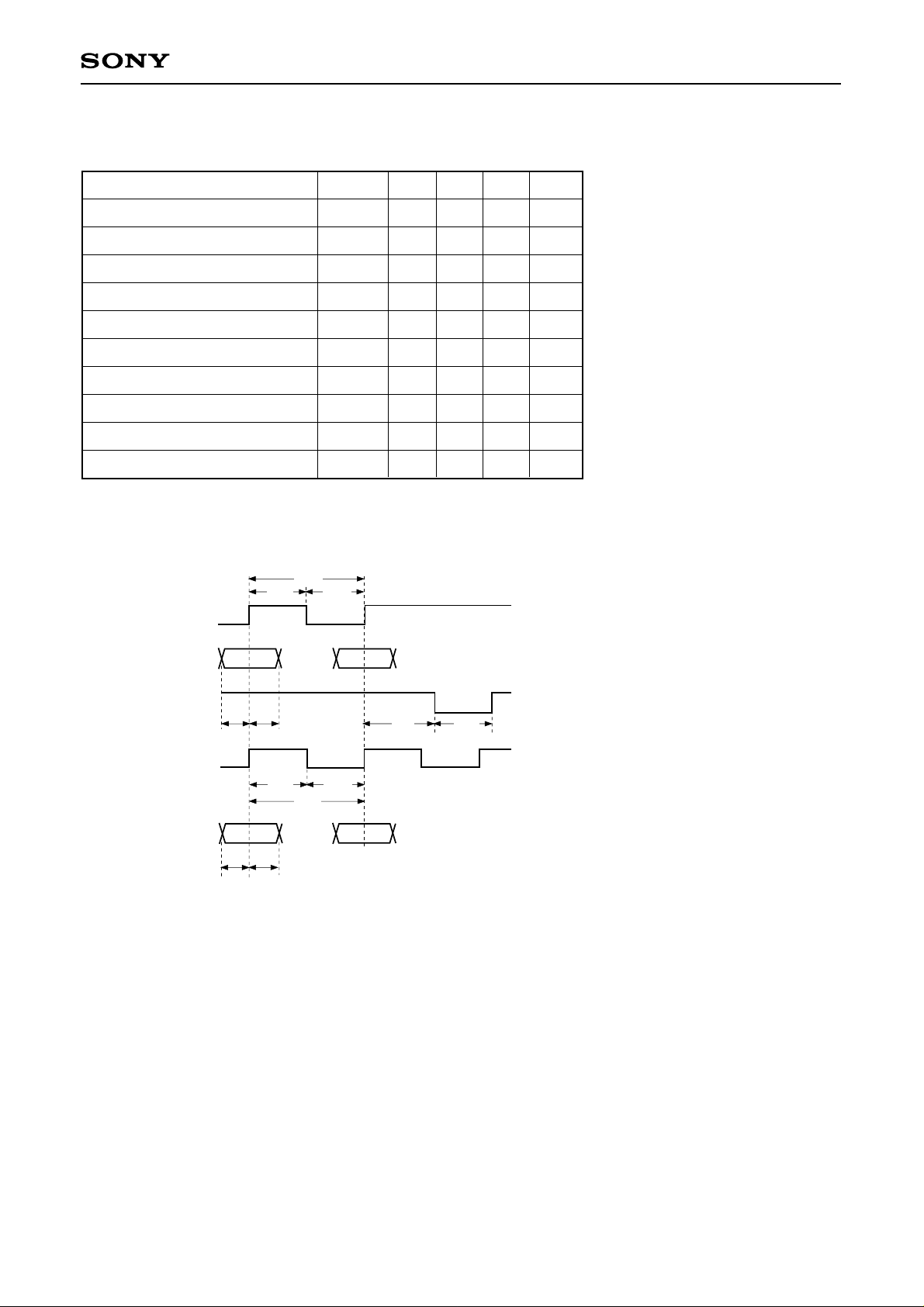
(2) CLOK, DATA, XLAT, SQCK and EXCK pins
(VDD = AVDD = 3.3V ±10%, VSS = AVSS = 0V, Topr = –20 to +75°C)
Item Symbol Min. Typ. Max. Unit
CXD3005R
Clock frequency
Clock pulse width
Setup time
Hold time
Delay time
Latch pulse width
EXCK SQCK frequency
EXCK SQCK pulse width
CNIN frequency
CNIN pulse width
∗
Only when $44 and $45 are executed.
CLOK
DATA
∗
∗
1/fCK
tWCK tWCK
fCK
tWCK
tSU
tH
tD
tWL
fT
tWT
fT
tWT
30
30
30
30
750
750
7.5
16
0.65
65
MHz
ns
ns
ns
ns
ns
MHz
ns
kHz
µs
XLAT
EXCK
SQCK
CNIN
SBSO
SQSO
tSU
tSU
tH
tWT tWT
1/fT
tH
tD
tWL
– 11 –
(3) SCLK pin
CXD3005R
XLAT
tSPWtDLS
SCLK
Serial Read Out Data
(SENS)
Item Symbol Min. Typ. Max. Unit
SCLK frequency
SCLK pulse width
Delay time
fSCLK
tSPW
tDLS
(4) COUT, MIRR and DFCT pins
Operating frequency
(VDD = AVDD = 3.3V ±10%, VSS = AVSS = 0V, Topr = –20 to +75°C)
Item Symbol Min. Typ. Max. Unit
COUT maximum operating frequency
MIRR maximum operating frequency
DFCT maximum operating frequency
31.3
15
fCOUT
fMIRR
fDFCTH
1/fSCLK
MSB LSB•••
16 MHz
ns
µs
40
40
5
kHz
kHz
kHz
•••
Conditions
∗1
∗2
∗3
∗
1
When using a high-speed traverse TZC.
∗
2
B
A
When the RF signal continuously satisfies the following conditions during the above traverse.
• A = 0.11VDD to 0.23VDD
B
• ≤ 25%
A + B
∗
3
During complete RF signal omission.
When settings related to DFCT signal generation are Typ.
– 12 –
(5) BCKI, LRCKI and PCMDI pins (VDD = 3.3V ±10%, Topr = –20 to +75°C)
Item Symbol Min. Typ. Max. Unit
CXD3005R
Input BCKI frequency
Input BCKI pulse width
Input data setup time
Input data hold time
Input LRCK setup time
Input LRCK hold time
BCKI
PCMDI
tBCK
tWIB
tIDS
tIDH
tILRH
tILRS
100
10
15
10
15
tWIB tWIB
tIDHtIDS
tILRH
4.5 MHz
ns
50%
tILRS
LRCKI
– 13 –
CXD3005R
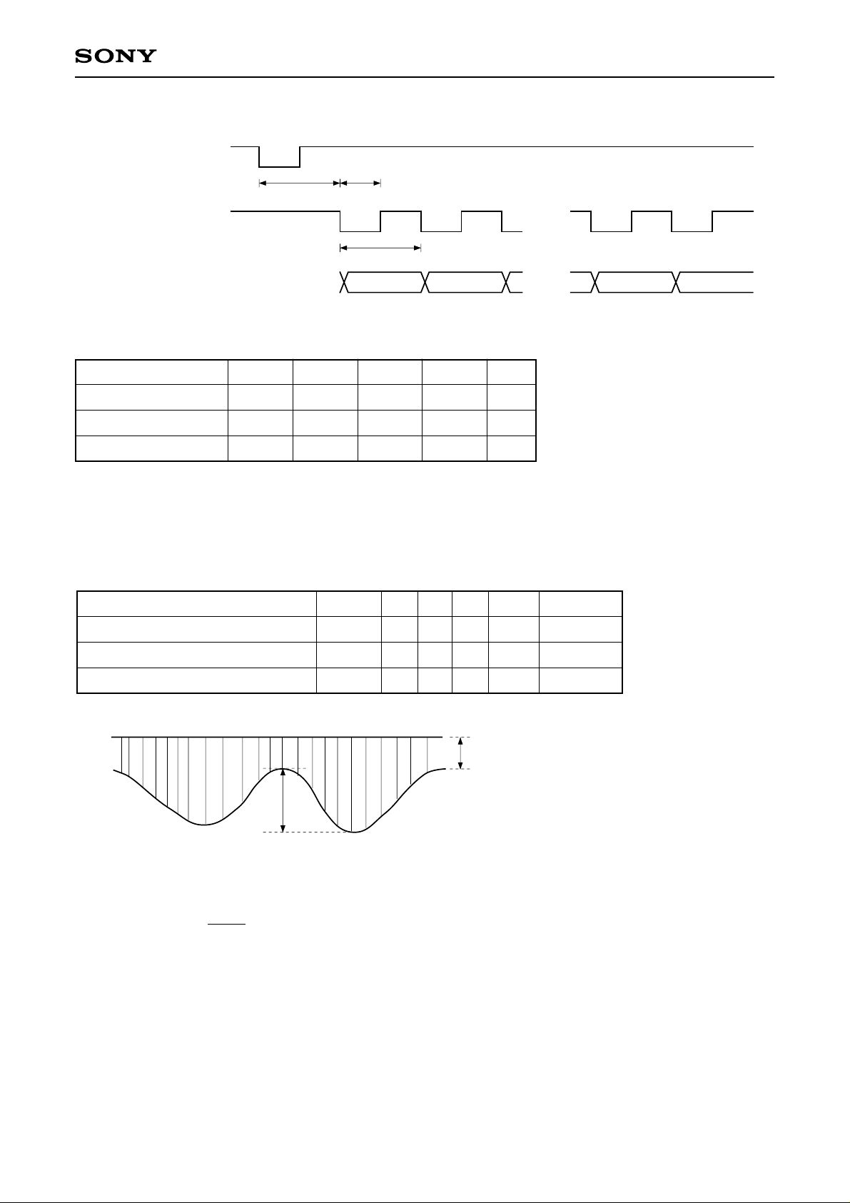
DAC Analog Characteristics
Measurement conditions
(Ta = 25°C, VDD = 3.3V, Fs = 44.1kHz, signal frequency = 1kHz, measurement band = 4Hz to 20kHz, master clock = 768Fs)
Item
S/N ratio
THD + N
Dynamic range
Channel separation
Output level
Difference in gain between channels
∗1
Using "A" weighting filter
∗2
–60 dB, 1kHz input
Typ.
93
0.015
91
91
1.70
0.1
Unit
dB
%
dB
dB
V (rms)
dB
(EIAJ)
(EIAJ)
(EIAJ)
(EIAJ)
The analog characteristics measurement circuit is shown below.
CXD3005R
AO1F
AO1R
3.9k
130k
3.9k
3.9k
130k
3.9k
47p
47p
4.7k
4.7k
4.7k
820p
4.7k
4.7k 4.7k
1800p 82p
820p
Remarks
∗
1
∗
1, ∗2
0.015
4.7k
22
100
OUTPUT
12k
TEST DISK
AO1F
AO1R
DATA
CXD3005R
AO2F
AO2R
Audio Circuit
Block diagram of analog characteristics measurement
– 14 –
SHIBASOKU (AM51A)768fs
Analog
1ch
Audio Analyzer
2ch

CXD3005R
Contents
[1] CPU Interface
§1-1. CPU Interface Timing ........................................................................................................................ 16
§1-2. CPU Interface Command Table ........................................................................................................ 16
§1-3. CPU Command Presets .................................................................................................................... 26
§1-4. Description of SENS Signals ............................................................................................................. 31
[2] Subcode Interface
§2-1. P to W Subcode Readout .................................................................................................................. 65
§2-2. 80-bit Sub Q Readout ........................................................................................................................ 65
[3] Description of Modes
§3-1. CLV-N Mode ...................................................................................................................................... 71
§3-2. CLV-W Mode ..................................................................................................................................... 71
§3-3. CAV-W Mode ..................................................................................................................................... 71
[4] Description of Other Functions
§4-1. Channel Clock Regeneration by the Digital PLL Circuit .................................................................... 73
§4-2. Frame Sync Protection ...................................................................................................................... 75
§4-3. Error Correction ................................................................................................................................. 75
§4-4. DA Interface ....................................................................................................................................... 76
§4-5. Digital Out .......................................................................................................................................... 79
§4-6. Servo Auto Sequence ....................................................................................................................... 80
§4-7. Digital CLV ......................................................................................................................................... 88
§4-8. Playback Speed ................................................................................................................................ 89
§4-9. DAC Block Playback Speed .............................................................................................................. 90
§4-10. DAC Block Input Timing .................................................................................................................... 90
§4-11. Asymmetry Compensation ................................................................................................................ 91
§4-12. CXD3005 Clock System .................................................................................................................... 92
[5] Description of Servo Signal Processing System Functions and Commands
§5-1. General Description of the Servo Signal Processing System ............................................................ 93
§5-2. Digital Servo Block Master Clock (MCK) ........................................................................................... 94
§5-3. AVRG Measurement and Compensation .......................................................................................... 94
§5-4. E:F Balance Adjustment Function ..................................................................................................... 96
§5-5. FCS Bias Adjustment Function .......................................................................................................... 96
§5-6. AGCNTL Function ............................................................................................................................. 98
§5-7. FCS Servo and FCS Search ........................................................................................................... 100
§5-8. TRK and SLD Servo Control ........................................................................................................... 101
§5-9. MIRR and DFCT Signal Generation ................................................................................................ 102
§5-10. DFCT Countermeasure Circuit ........................................................................................................ 103
§5-11. Anti-Shock Circuit ............................................................................................................................ 103
§5-12. Brake Circuit .................................................................................................................................... 104
§5-13. COUT Signal ................................................................................................................................... 105
§5-14. Serial Readout Circuit ...................................................................................................................... 105
§5-15. Writing to the Coefficient RAM ........................................................................................................ 106
§5-16. PWM Output .................................................................................................................................... 106
§5-17. DIRC Input Pin ................................................................................................................................. 108
§5-18. Servo Status Changes Produced by the LOCK Signal ................................................................... 109
§5-19. Description of Commands and Data Sets ....................................................................................... 109
§5-20. List of Servo Filter Coefficients ........................................................................................................ 124
§5-21. Filter Composition ............................................................................................................................ 126
§5-22. TRACKING and FOCUS Frequency Response .............................................................................. 133
[6] Application Circuit .................................................................................................................................. 134
Explanation of abbreviations AVRG: Average
AGCNTL: Auto gain control
FCS: Focus
TRK: Tracking
SLD: Sled
DFCT: Defect
– 15 –
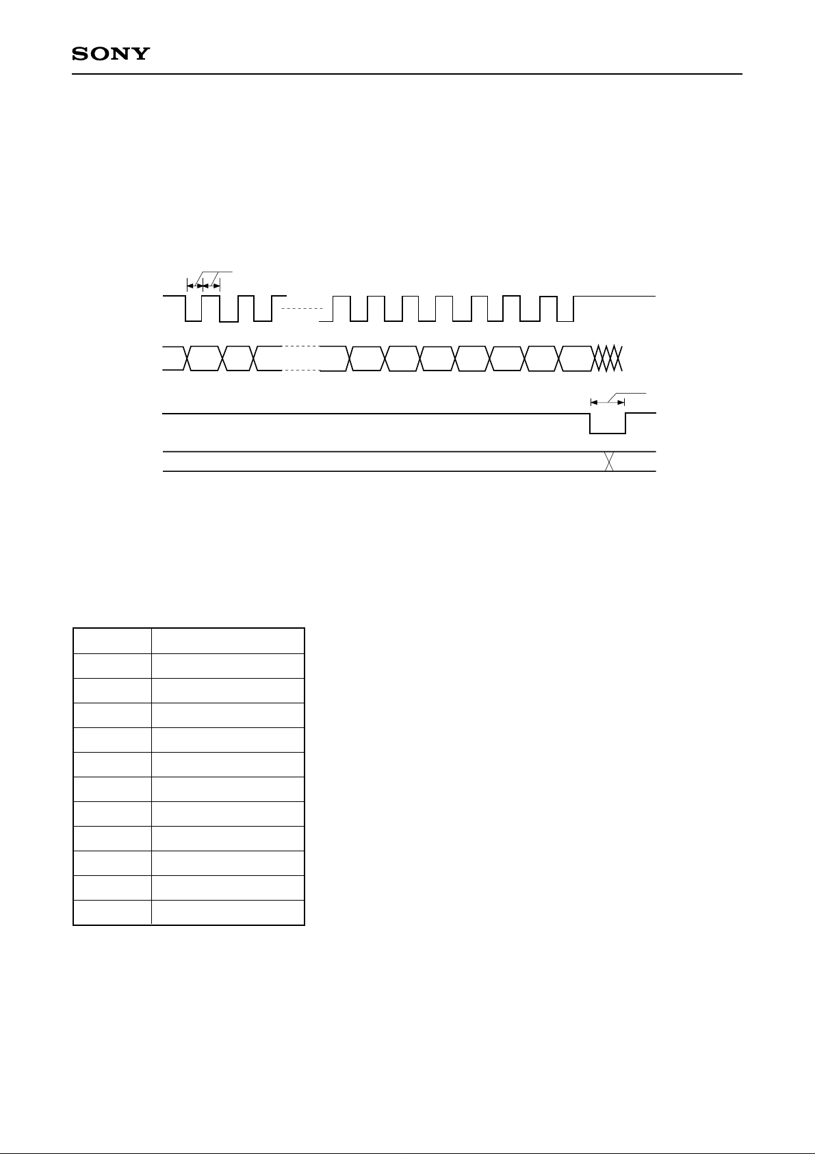
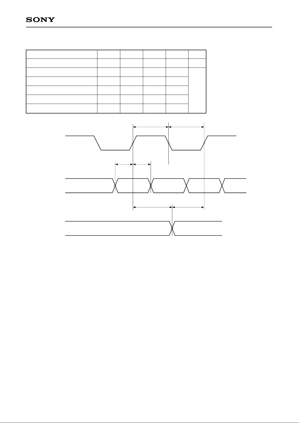
[1] CPU Interface
§1-1. CPU Interface Timing
• CPU interface
This interface uses DATA, CLOK and XLAT to set the modes.
The interface timing chart is shown below.
30ns or more
CLOK
CXD3005R
DATA
XLAT
Registers
D0 D1
D18 D19 D20 D21 D22 D23
• The internal registers are initialized by a reset when XRST = 0.
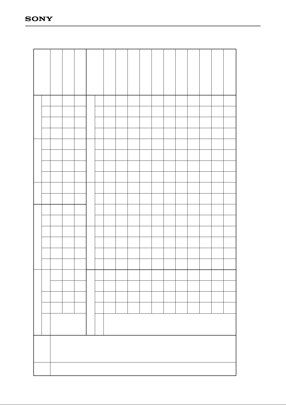
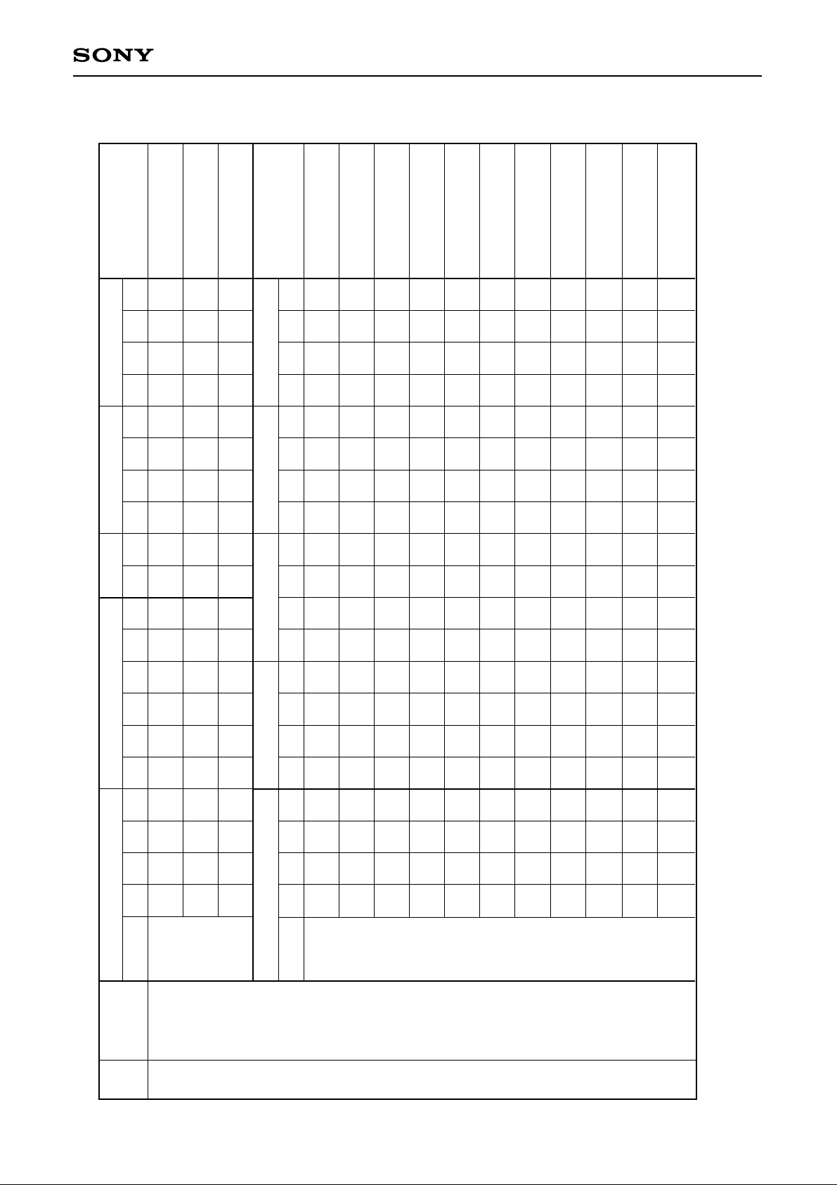
§1-2. CPU Interface Command Table
Total bit length for each register
Register
0 to 2
3
4 to 6
7
Total bit length
8 bits
8 to 24 bits
16 bits
20 bits
750ns or more
Valid
8
9
A
B
C
D
E
24 bits
20 bits
28 bits
20 bits
16 bits
20 bits
20 bits
– 16 –
FOCUS SERVO ON
(FOCUS GAIN
NORMAL)
FOCUS SERVO ON
(FOCUS GAIN
DOWN)
FOCUS SERVO OFF,
0V OUT
FOCUS SERVO OFF,
FOCUS SEARCH
VOLTAGE OUT
FOCUS SEARCH
VOLTAGE DOWN
FOCUS SEACH
VOLTAGE UP
ANTI SHOCK ON
ANTI SHOCK OFF
BRAKE ON
BRAKE OFF
TRACKING GAIN
NORMAL
TRACKING GAIN UP
TRACKING GAIN UP
CXD3005R
—: Don’t care
FILTER SELECT 1
TRACKING GAIN UP
FILTER SELECT 2
Data 5
Data 4
Data 3
D3 D2 D1 D0
D6 D5 D4
D7
D10 D9 D8
D11
—
—
—
—
—
—
—
—
—
—
—
—
—
—
—
—
—
—
—
—
—
—
—
—
—
—
—
—
—
—
—
—
—
—
—
—
—
—
—
—
—
—
—
—
—
—
—
—
—
—
—
—
—
—
—
—
—
—
—
—
—
—
—
—
—
—
—
—
—
—
—
—
—
—
—
—
—
—
—
—
—
—
—
—
—
—
—
—
—
—
—
—
—
—
—
—
—
—
—
—
—
—
—
—
—
—
—
—
—
—
—
—
—
—
—
—
—
—
—
—
—
—
—
—
—
—
—
—
—
—
—
—
—
—
—
—
—
—
—
—
—
—
—
—
—
—
—
—
—
—
—
—
—
—
—
—
—
—
—
—
—
—
—
—
—
—
—
—
—
—
—
—
—
—
—
—
—
—
—
—
—
—
—
D13 D12
Data 2
Data 1
Address
Command
Command Table ($0X to 1X)
Register
—
—
D15 D14
—
—
D17 D16
0
1
D19 D18
D23 to D20
—
—
—
—
—
1
1
—
—
—
—
0
—
0
0 0 0 0
FOCUS
CONTROL
0
—
—
—
—
1
—
0
—
—
—
—
—
—
—
—
—
—
—
—
—
—
—
—
—
—
—
—
—
—
—
—
—
—
—
—
—
—
0
1
—
—
—
—
—
1
1
—
—
—
—
0
0
—
0
1
1
—
0
—
—
0
—
0 0 0 1
TRACKING
CONTROL
1
0
—
—
1
—
1
—
—
0
—
—
—
—
—
—
– 17 –
TRACKING SERVO OFF
TRACKING SERVO ON
FORWARD TRACK JUMP
REVERSE TRACK JUMP
—
—
—
—
—
—
—
—
SLED SERVO OFF
SLED SERVO ON
FORWARD SLED MOVE
—
—
—
—
—
—
REVERSE SLED MOVE
—
—
(±1 × basic value) (Default)
SLED KICK LEVEL
—
—
basic value)
basic value)
×
SLED KICK LEVEL
(±2
SLED KICK LEVEL
—
—
—
—
basic value)
×
×
(±3
SLED KICK LEVEL
(±4
—
—
CXD3005R
—: Don’t care
Data 5
Data 4
Data 3
Data 2
D3 D2 D1 D0
D6 D5 D4
D7
D10 D9 D8
D11
D13 D12
—
—
—
—
—
—
—
—
—
—
—
—
—
—
—
—
—
—
—
—
—
—
—
—
—
—
—
—
—
—
—
—
—
—
—
—
—
—
—
—
—
—
—
—
—
—
—
—
—
—
—
—
—
—
—
—
—
—
—
—
—
—
—
—
—
—
—
—
—
—
—
—
—
—
—
—
—
—
—
—
—
—
—
—
—
—
—
—
—
—
—
Data 5
—
—
—
—
Data 4
—
—
—
—
Data 3
—
—
—
—
Data 2
—
D3 D2 D1 D0
D6 D5 D4
D7
D10 D9 D8
D11
D13 D12
—
—
—
—
—
—
—
—
—
—
—
—
—
—
—
—
—
—
—
—
—
—
—
—
—
—
—
—
—
—
—
—
—
—
—
—
—
—
—
—
—
—
—
—
—
—
—
—
—
—
—
—
—
—
D15 D14
—
—
D17 D16
Data 1
Address
Command
Command Table ($2X to 3X)
Register
0
0
D19 D18
D23 to D20
—
—
—
—
—
1
0
0
1
—
—
—
1
1
0 0 1 0
TRACKING
MODE
2
—
—
—
—
0
1
0
1
0
0
1
—
—
—
—
—
—
Data 1
1
—
—
Address
D15 D14
D17 D16
D19 D18
D23 to D20
Command
Register
—
—
—
—
0
1
0
1
0
0
1
1
0
0
0
0
0
0
0
0
0 0 1 1
SELECT
3
– 18 –

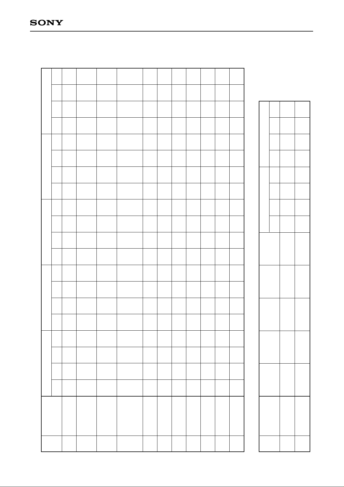
Data 2
KRAM DATA (K00)
SLED INPUT GAIN
KRAM DATA (K01)
KD0
KD1
D2 D1 D0
KD2
SLED LOW BOOST FILTER A-H
KRAM DATA (K02)
SLED LOW BOOST FILTER A-L
KRAM DATA (K03)
SLED LOW BOOST FILTER B-H
KRAM DATA (K04)
SLED LOW BOOST FILTER B-L
KRAM DATA (K05)
KD0
KD0
KD0
KD0
KD0
KD1
KD1
KD1
KD1
KD1
KD2
KD2
KD2
KD2
KD2
SLED OUTPUT GAIN
KRAM DATA (K06)
FOCUS INPUT GAIN
KRAM DATA (K07)
SLED AUTO GAIN
KRAM DATA (K08)
KD0
KD0
KD1
KD1
KD2
KD2
FOCUS HIGH CUT FILTER A
KRAM DATA (K09)
FOCUS HIGH CUT FILTER B
KRAM DATA (K0A)
FOCUS LOW BOOST FILTER A-H
KRAM DATA (K0B)
FOCUS LOW BOOST FILTER A-L
KD0
KD0
KD0
KD0
KD1
KD1
KD1
KD1
KD2
KD2
KD2
KD2
CXD3005R
KRAM DATA (K0C)
FOCUS LOW BOOST FILTER B-H
KRAM DATA (K0D)
FOCUS LOW BOOST FILTER B-L
KRAM DATA (K0E)
FOCUS PHASE COMPENSATE FILTER A
KRAM DATA (K0F)
FOCUS DEFECT HOLD GAIN
KD0
KD0
KD0
KD0
KD1
KD1
KD1
KD1
KD2
KD2
KD2
KD2
D3
Data 1
D6 D5 D4
D7
D9 D8
Address 4
D11 D10
Address 3
D15 to D12
Address 2
D19 to D16
KD3
KD4
KD5
KD6
KD7
0
0
0
0
KD3
KD4
KD5
KD6
KD7
1
0
0
0
KD3
KD4
KD5
KD6
KD7
0
1
0
0
KD3
KD4
KD5
KD6
KD7
1
1
0
0
KD3
KD4
KD5
KD6
KD7
0
0
1
0
KD3
KD4
KD5
KD6
KD7
1
0
1
0
KD3
KD4
KD5
KD6
KD7
0
1
1
0
KD3
KD4
KD5
KD6
KD7
1
1
1
0
KD3
KD4
KD5
KD6
KD7
0
0
0
1
0 0 0 0SELECT
0 1 0 0
KD3
KD4
KD5
KD6
KD7
1
0
0
1
KD3
KD4
KD5
KD6
KD7
0
1
0
1
KD3
KD4
KD5
KD6
KD7
1
1
0
1
KD3
KD4
KD5
KD6
KD7
0
0
1
1
KD3
KD4
KD5
KD6
KD7
1
0
1
1
KD3
KD4
KD5
KD6
KD7
0
1
1
1
KD3
KD4
KD5
KD6
KD7
1
1
1
1
Address 1
D23 to D20
Command
Command Table ($340X)
Register
0 0 1 1
3
– 19 –

Data 2
KRAM DATA (K10)
FOCUS PHASE COMPENSATE FILTER B
KRAM DATA (K11)
FOCUS OUTPUT GAIN
KRAM DATA (K12)
ANTI SHOCK INPUT GAIN
KRAM DATA (K13)
FOCUS AUTO GAIN
KRAM DATA (K14)
KD0
KD0
KD0
KD0
KD1
KD1
KD1
KD1
D2 D1 D0
KD2
KD2
KD2
KD2
HPTZC / AUTO GAIN HIGH PASS FILTER A
KRAM DATA (K15)
HPTZC / AUTO GAIN HIGH PASS FILTER B
KRAM DATA (K16)
ANTI SHOCK HIGH PASS FILTER A
KRAM DATA (K17)
HPTZC / AUTO GAIN LOW PASS FILTER B
KRAM DATA (K18)
FIX
KRAM DATA (K19)
TRACKING INPUT GAIN
KRAM DATA (K1A)
KD0
KD0
KD0
KD0
KD0
KD0
KD1
KD1
KD1
KD1
KD1
KD1
KD2
KD2
KD2
KD2
KD2
KD2
TRACKING HIGH CUT FILTER A
KRAM DATA (K1B)
TRACKING HIGH CUT FILTER B
KRAM DATA (K1C)
TRACKING LOW BOOST FILTER A-H
KRAM DATA (K1D)
TRACKING LOW BOOST FILTER A-L
KRAM DATA (K1E)
TRACKING LOW BOOST FILTER B-H
KD0
KD0
KD0
KD0
KD0
KD1
KD1
KD1
KD1
KD1
KD2
KD2
KD2
KD2
KD2
CXD3005R
KRAM DATA (K1F)
TRACKING LOW BOOST FILTER B-L
KD0
KD1
KD2
D3
Data 1
D6 D5 D4
D7
D9 D8
Address 4
D11 D10
Address 3
D15 to D12
Address 2
D19 to D16
KD3
KD4
KD5
KD6
KD7
0
0
0
0
KD3
KD4
KD5
KD6
KD7
1
0
0
0
KD3
KD4
KD5
KD6
KD7
0
1
0
0
KD3
KD4
KD5
KD6
KD7
1
1
0
0
KD3
KD4
KD5
KD6
KD7
0
0
1
0
KD3
KD4
KD5
KD6
KD7
1
0
1
0
KD3
KD4
KD5
KD6
KD7
0
1
1
0
KD3
KD4
KD5
KD6
KD7
1
1
1
0
KD3
KD4
KD5
KD6
KD7
0
0
0
1
0 0 0 1SELECT
0 1 0 0
KD3
KD4
KD5
KD6
KD7
1
0
0
1
KD3
KD4
KD5
KD6
KD7
0
1
0
1
KD3
KD4
KD5
KD6
KD7
1
1
0
1
KD3
KD4
KD5
KD6
KD7
0
0
1
1
KD3
KD4
KD5
KD6
KD7
1
0
1
1
KD3
KD4
KD5
KD6
KD7
0
1
1
1
KD3
KD4
KD5
KD6
KD7
1
1
1
1
Address 1
D23 to D20
Command
Command Table ($341X)
Register
0 0 1 1
3
– 20 –

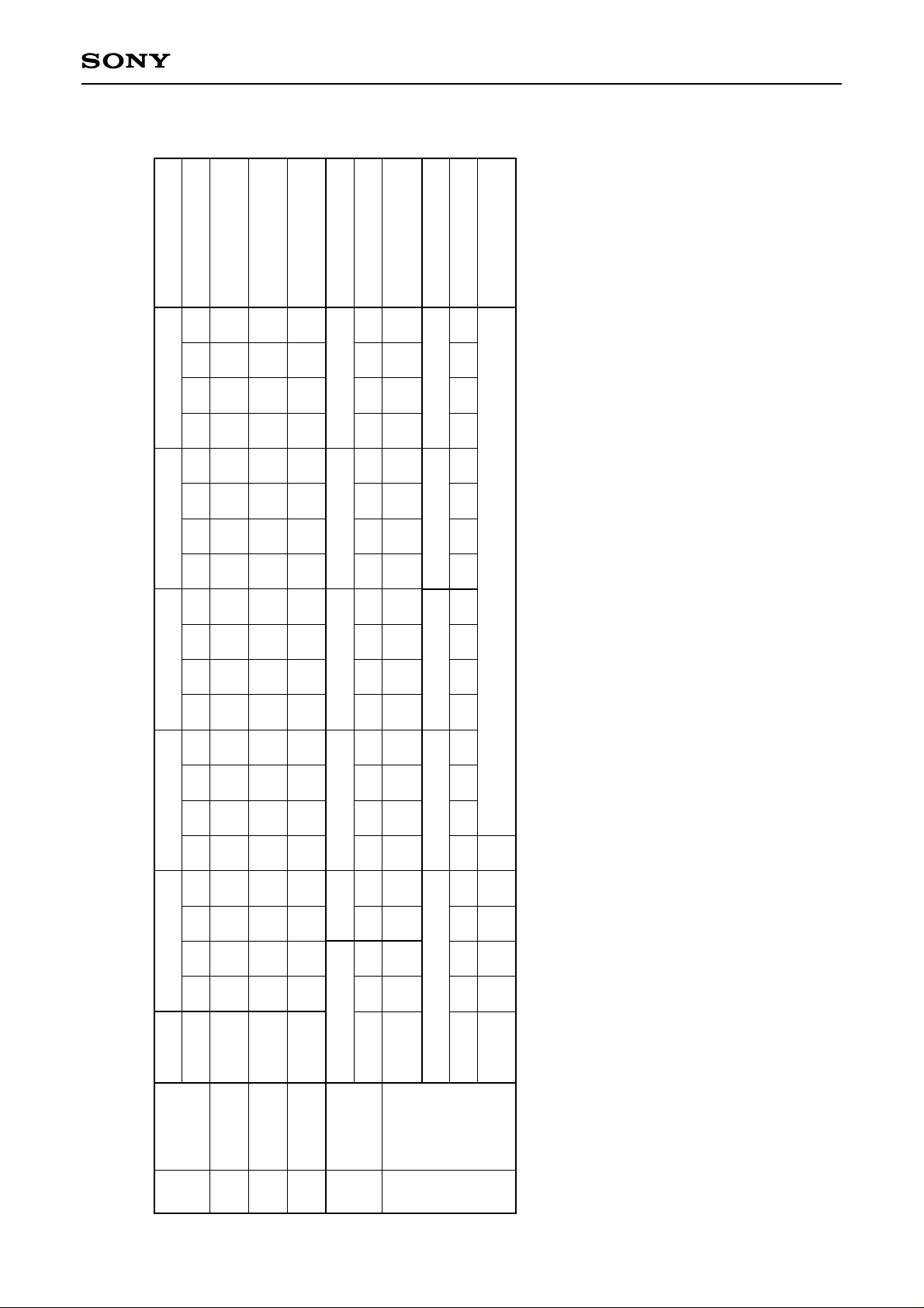
Data 2
KRAM DATA (K20)
TRACKING PHASE COMPENSATE FILTER A
KRAM DATA (K21)
TRACKING PHASE COMPENSATE FILTER B
KRAM DATA (K22)
TRACKING OUTPUT GAIN
KRAM DATA (K23)
TRACKING AUTO GAIN
KRAM DATA (K24)
FOCUS GAIN DOWN HIGH CUT FILTER A
KD0
KD0
KD0
KD0
KD0
KD1
KD1
KD1
KD1
KD1
D2 D1 D0
KD2
KD2
KD2
KD2
KD2
KRAM DATA (K25)
FOCUS GAIN DOWN HIGH CUT FILTER B
KRAM DATA (K26)
FOCUS GAIN DOWN LOW BOOST FILTER A-H
KRAM DATA (K27)
FOCUS GAIN DOWN LOW BOOST FILTER A-L
KRAM DATA (K28)
FOCUS GAIN DOWN LOW BOOST FILTER B-H
KRAM DATA (K29)
FOCUS GAIN DOWN LOW BOOST FILTER B-L
KRAM DATA (K2A)
FOCUS GAIN DOWN PHASE COMPENSATE FILTER A
KD0
KD0
KD0
KD0
KD0
KD0
KD1
KD1
KD1
KD1
KD1
KD1
KD2
KD2
KD2
KD2
KD2
KD2
CXD3005R
KRAM DATA (K2B)
FOCUS GAIN DOWN DEFECT HOLD GAIN
KRAM DATA (K2C)
FOCUS GAIN DOWN PHASE COMPENSATE FILTER B
KRAM DATA (K2D)
FOCUS GAIN DOWN OUTPUT GAIN
KRAM DATA (K2E)
NOT USED
KRAM DATA (K2F)
NOT USED
KD0
KD0
KD0
KD0
KD0
KD1
KD1
KD1
KD1
KD1
KD2
KD2
KD2
KD2
KD2
D3
Data 1
D6 D5 D4
D7
D9 D8
Address 4
D11 D10
Address 3
D15 to D12
Address 2
D19 to D16
KD3
KD4
KD5
KD6
KD7
0
0
0
0
KD3
KD4
KD5
KD6
KD7
1
0
0
0
KD3
KD4
KD5
KD6
KD7
0
1
0
0
KD3
KD4
KD5
KD6
KD7
1
1
0
0
KD3
KD4
KD5
KD6
KD7
0
0
1
0
KD3
KD4
KD5
KD6
KD7
1
0
1
0
KD3
KD4
KD5
KD6
KD7
0
1
1
0
KD3
KD4
KD5
KD6
KD7
1
1
1
0
KD3
KD4
KD5
KD6
KD7
0
0
0
1
0 0 1 0SELECT
0 1 0 0
KD3
KD4
KD5
KD6
KD7
1
0
0
1
KD3
KD4
KD5
KD6
KD7
0
1
0
1
KD3
KD4
KD5
KD6
KD7
1
1
0
1
KD3
KD4
KD5
KD6
KD7
0
0
1
1
KD3
KD4
KD5
KD6
KD7
1
0
1
1
KD3
KD4
KD5
KD6
KD7
0
1
1
1
KD3
KD4
KD5
KD6
KD7
1
1
1
1
Address 1
D23 to D20
Command
Register
Command Table ($342X)
0 0 1 1
3
– 21 –
Data 2
KRAM DATA (K30)
FIX
KRAM DATA (K31)
KD0
KD1
D2 D1 D0
KD2
ANTI SHOCK LOW PASS FILTER B
KRAM DATA (K32)
NOT USED
KRAM DATA (K33)
ANTI SHOCK HIGH PASS FILTER B-H
KRAM DATA (K34)
ANTI SHOCK HIGH PASS FILTER B-L
KRAM DATA (K35)
ANTI SHOCK FILTER COMPARATE GAIN
KD0
KD0
KD0
KD0
KD0
KD1
KD1
KD1
KD1
KD1
KD2
KD2
KD2
KD2
KD2
KRAM DATA (K36)
TRACKING GAIN UP2 HIGH CUT FILTER A
KRAM DATA (K37)
TRACKING GAIN UP2 HIGH CUT FILTER B
KRAM DATA (K38)
TRACKING GAIN UP2 LOW BOOST FILTER A-H
KRAM DATA (K39)
TRACKING GAIN UP2 LOW BOOST FILTER A-L
KRAM DATA (K3A)
TRACKING GAIN UP2 LOW BOOST FILTER B-H
KRAM DATA (K3B)
TRACKING GAIN UP2 LOW BOOST FILTER B-L
KD0
KD0
KD0
KD0
KD0
KD0
KD1
KD1
KD1
KD1
KD1
KD1
KD2
KD2
KD2
KD2
KD2
KD2
CXD3005R
KRAM DATA (K3C)
TRACKING GAIN UP PHASE COMPENSATE FILTER A
KRAM DATA (K3D)
TRACKING GAIN UP PHASE COMPENSATE FILTER B
KRAM DATA (K3E)
TRACKING GAIN UP OUTPUT GAIN
KRAM DATA (K3F)
NOT USED
KD0
KD0
KD0
KD0
KD1
KD1
KD1
KD1
KD2
KD2
KD2
KD2
D3
Data 1
D6 D5 D4
D7
D9 D8
Address 4
D11 D10
Address 3
D15 to D12
Address 2
D19 to D16
KD3
KD4
KD5
KD6
KD7
0
0
0
0
KD3
KD4
KD5
KD6
KD7
1
0
0
0
KD3
KD4
KD5
KD6
KD7
0
1
0
0
KD3
KD4
KD5
KD6
KD7
1
1
0
0
KD3
KD4
KD5
KD6
KD7
0
0
1
0
KD3
KD4
KD5
KD6
KD7
1
0
1
0
KD3
KD4
KD5
KD6
KD7
0
1
1
0
KD3
KD4
KD5
KD6
KD7
1
1
1
0
KD3
KD4
KD5
KD6
KD7
0
0
0
1
0 0 1 1SELECT
0 1 0 0
KD3
KD4
KD5
KD6
KD7
1
0
0
1
KD3
KD4
KD5
KD6
KD7
0
1
0
1
KD3
KD4
KD5
KD6
KD7
1
1
0
1
KD3
KD4
KD5
KD6
KD7
0
0
1
1
KD3
KD4
KD5
KD6
KD7
1
0
1
1
KD3
KD4
KD5
KD6
KD7
0
1
1
1
KD3
KD4
KD5
KD6
KD7
1
1
1
1
Address 1
D23 to D20
Command
Command Table ($343X)
Register
0 0 1 1
3
– 22 –

Data 2
KRAM DATA (K40)
TRACKING HOLD FILTER INPUT GAIN
KRAM DATA (K41)
TRACKING HOLD FILTER A-H
KRAM DATA (K42)
TRACKING HOLD FILTER A-L
KRAM DATA (K43)
TRACKING HOLD FILTER B-H
KD0
KD0
KD0
KD0
KD1
KD1
KD1
KD1
D2 D1 D0
KD2
KD2
KD2
KD2
KRAM DATA (K44)
TRACKING HOLD FILTER B-L
KRAM DATA (K45)
TRACKING HOLD FILTER OUTPUT GAIN
KRAM DATA (K46)
NOT USED
KRAM DATA (K47)
NOT USED
KD0
KD0
KD0
KD0
KD1
KD1
KD1
KD1
KD2
KD2
KD2
KD2
KRAM DATA (K48)
FOCUS HOLD FILTER INPUT GAIN
KRAM DATA (K49)
FOCUS HOLD FILTER A-H
KRAM DATA (K4A)
FOCUS HOLD FILTER A-L
KRAM DATA (K4B)
FOCUS HOLD FILTER B-H
KRAM DATA (K4C)
FOCUS HOLD FILTER B-L
KD0
KD0
KD0
KD0
KD0
KD1
KD1
KD1
KD1
KD1
KD2
KD2
KD2
KD2
KD2
CXD3005R
KRAM DATA (K4D)
FOCUS HOLD FILTER OUTPUT GAIN
KRAM DATA (K4E)
NOT USED
KRAM DATA (K4F)
NOT USED
KD0
KD0
KD0
KD1
KD1
KD1
KD2
KD2
KD2
D3
Data 1
D6 D5 D4
D7
D9 D8
Address 4
D11 D10
Address 3
D15 to D12
Address 2
D19 to D16
KD3
KD4
KD5
KD6
KD7
0
0
0
0
KD3
KD4
KD5
KD6
KD7
1
0
0
0
KD3
KD4
KD5
KD6
KD7
0
1
0
0
KD3
KD4
KD5
KD6
KD7
1
1
0
0
KD3
KD4
KD5
KD6
KD7
0
0
1
0
KD3
KD4
KD5
KD6
KD7
1
0
1
0
KD3
KD4
KD5
KD6
KD7
0
1
1
0
KD3
KD4
KD5
KD6
KD7
1
1
1
0
KD3
KD4
KD5
KD6
KD7
0
0
0
1
0 1 0 0SELECT
0 1 0 0
KD3
KD4
KD5
KD6
KD7
1
0
0
1
KD3
KD4
KD5
KD6
KD7
0
1
0
1
KD3
KD4
KD5
KD6
KD7
1
1
0
1
KD3
KD4
KD5
KD6
KD7
0
0
1
1
KD3
KD4
KD5
KD6
KD7
1
0
1
1
KD3
KD4
KD5
KD6
KD7
0
1
1
1
KD3
KD4
KD5
KD6
KD7
1
1
1
1
Address 1
D23 to D20
Command
Register
Command Table ($344X)
0 0 1 1
3
– 23 –
FOCUS BIAS LIMIT
FOCUS BIAS DATA
TRVSC DATA
FOCUS SEARCH SPEED/
VOLTAGE/AUTO GAIN
DTZC/TRACK JUMP
VOLTAGE/AUTO GAIN
FZSL/SLED MOVE/
Voltage/AUTO GAIN
LEVEL/AUTO GAIN/
DFSW/ (Initialize)
SERIAL DATA READ
MODE/SELECT
FOCUS BIAS
Operation for MIRR/
DFCT/FOK
TZC/COUT
BOTTOM/MIRR
SLED FILTER
Filter
CXD3005R
—: Don’t care
Others
Data 3
D3 D2 D1 D0
Data 2
D6 D5 D4
D7
Data 1
D10 D9 D8
D11
Address 2
D13 D12
D15 D14
—
FBL1
FBL2
FBL3
FBL4
FBL5
FBL6
FBL7
FBL8
FBL9
0
1
1
1
1
1
0
—
FB1
FB2
FB3
FB4
FB5
FB6
FB7
FB8
FB9
1
0
1
1
1
1
0
TV0
TV1
TV2
TV3
TV4
TV5
TV6
TV7
TV8
TV9
0
0
1
1
1
1
0
Data 4
Data 3
Data 2
Data 1
D3 D2 D1 D0
D6 D5 D4
D7
D10 D9 D8
D11
D13 D12
D15 D14
FG0
FG1
FG2
FG3
FG4
FG5
FG6
FTZ
FS0
FS1
FS2
FS3
FS4
FS5
FT0
FT1
1
TG0
TG1
TG2
TG3
TG4
TG5
TG6
SFJP
TJ0
TJ1
TJ2
TJ3
TJ4
TJ5
DTZC
TDZC
0
AGHT
AGHS
AGV2
AGV1
AGGT
AGGF
AGJ
AGS
SM0
SM1
SM2
SM3
SM4
SM5
FZSL
FZSH
1
TLC0
TLC1
TLC2
FLC1
TCLM
TBLM
LKSW
DFSW
AGT
AGF
RFLC
RFLM
FLC0
FLM
VCLC
VCLM
0
0
0
0
0
0
0
0
0
SD0
SD1
SD2
SD3
SD4
SD5
SD6
DAC
1
MTI0
INBK
SJHD
0
TPS0
TPS1
FPS0
FPS1
TJD0
0
FBV0
FBV1
FBUP
FBSS
FBON
0
0
0
0
0
RINT
D1V1
D1V2
D2V1
D2V2
BTF
SFOX
MAX1
MAX2
SDF1
SDF2
SFO1
SFO2
1
0
0
0
0
MRC0
MRC1
BTS0
BTS1
0
MOT2
COT1
COT2
CETF
CETZ
COTS
COSS
0
0
0
0
0
0
0
0
0
TLD0
TLD1
TLD2
0
THSK
THID
SFSK
SFID
1
XT1D
MIRI
MDFI
COIN
LKIN
0
TLCD
DFIS
T3UM
T3NM
T1UM
T1NM
F3DM
F3NM
F1DM
F1NM
0
0
AGHF
SRO0
SRO1
LPAS
FTQ
ASFG
0
DRR0
DRR1
DRR2
0
XT2D
XT4D
AGG4
0
1
0
0
1
0
0 0 1 1
0
1
0
Address
D17 D16
1
Address 1
Command
Register
Command Table ($34FX to 3FX)
0
D23 to D20 D19 D18
D17 D16
D23 to D20 D19 D18
0
1
1
0
0
1
1
0
0
1
1
1
1
1
0
0
0
0
1
1
1
1
0
0
0
1
1
1
1
1
1
1
1
0 0 1 1
SELECT
3
– 24 –
CXD3005R
Data 4
Data 3
Data 2
D9 D8
D12 D11 D10
D15 D14 D13
D17 D16
—
—
—
—
0
0
0
LSSL
MT0
MT1
MT2
—
—
—
—
0
0
0
0
0
0
0
—
—
—
—
0
0
0
0
KF0
KF1
KF2
1
2
4
8
16
32
64
128
256
512
1024
CS
VCO2
VCO2
THRU
CS0
VCO1
CS1
VC01
KSL0
KSL1
KSL2
KSL3
VCO
SEL2
SOCT
ASHS
PLM0
PLM1
PLM2
PLM3
0
0
ATT
DAC
DAC
EMP
XWOC
FLFC
SUB
BiliGL
AT1D0
AT1D1
AT1D2
AT1D3
AT1D4
AT1D5
AT1D6
AT1D7
SOC2
DADS
PCT2
1
2
4
8
16
32
64
128
256
512
1024
—
—
—
—
0
0
0
0
PCC0
PCC1
Gain
VP
VP
DCLV0
0
0
CTL0
CTL1
VP0
VP1
VP2
VP3
VP4
VP5
VP6
0
FCSW
Gain
CAV0
Gain
CAV1
VPON
LPWR
HIFC
VC2C
SFSL
ICAP
SPDC
—: Don’t care
Data 6
Data 5
D2 D1 D0
D5 D4 D3
D7 D6
—
— — —
SCSY 0
SEL
SCOR
ERC4
AT2D0
AT2D3 AT2D2 AT2D1
AT2D6 AT2D5 AT2D4
AT2D7
D20 D19 D18
Data 1
D23 D22 D21
Address
D26 D25 D24
D27
MT3
AS0
AS1
AS2
AS3
0
0
1
0
0
TR0
TR1
TR2
TR3
1
0
1
0
KF3
SD0
SD1
SD2
SD3
0
1
1
0
2048
4096
8192
16384
32768
1
1
1
0
SEL
VCO
WSEL
DOUT
Mute-F
Mute
DOUT
CD-
ROM
0
0
0
1
MAIN
BiliGL
DPLL
ON/OFF
ASEQ
ON/OFF
DSPB
ON/OFF
DCLV
ON/OFF
1
0
0
1
PCT1
ATT
Mute
0
0
0
1
0
1
2048
4096
8192
16384
32768
1
1
0
1
Gain
Gain
Gain
Gain
Gain
0
0
1
1
DCLV1
CLVS
MDS0
MDS1
MDP0
DCLV
MDP1
VP7
Gain
TP
TB
PWM MD
1
0
1
1
EPWM
CM0
CM1
CM2
CM3
0
1
1
1
Data 2 Data 3 Data 4
Address Data 1
1 0 0 0
1 0 1 0
Command
Auto sequence
Blind (A, E),
Brake (B),
Overflow (C, G)
Sled KICK,
4
Command Table ($4X to EX)
Register
5
BRAKE (D),
KICK (F)
Auto sequence
6
(N)
track jump
7
count setting
MODE
specification
8
Function
specification
9
– 25 –
Audio CTRL
Traverse monitor
counter setting
A
B
Spindle servo
coefficient setting
CLV CTRL
C
D
SPD mode
E
Command
MODE
Register
specification
Audio CTRL
8
A
FOCUS SERVO OFF,
0V OUT
TRACKING GAIN UP
FILTER SELECT 1
TRACKING SERVO OFF
SLED SERVO OFF
SLED KICK LEVEL
(±1 × basic value) (Default)
—: Don’t care
KRAM DATA
($3400XX to $344fXX)
CXD3005R
Data 5
Data 4
Data 3
D3 D2 D1 D0
D6 D5 D4
D7
D10 D9 D8
D11
D3 D2 D0 D0
D6 D5 D4
D7
D10 D9 D8
D11
—
— — —
— — —
—
— — —
Data 2
D3 D2 D0 D0
Data 1
D6 D5 D4
D7
Address 3
D10 D9 D8
D11
—
—
—
—
—
—
—
—
—
—
—
—
—
—
—
—
—
—
—
—
—
—
—
—
—
—
—
—
Data 5
—
—
—
—
Data 4
—
—
—
—
Data 3
—
—
—
—
D13 D12
Data 2
D15 D14
D17 D16
Data 1
D19 D18
Address
D23 to D20
Command
FOCUS
§1-3. CPU Command Presets
Command Preset Table ($0X to 34X)
Register
—
—
—
—
—
0
1
0
0
0
0
0
0
0 0 0 0
0 0 0 1
CONTROL
TRACKING
0
1
CONTROL
—
Data 2
—
—
0
Data 1
0
0
0
Address
0 0 1 0
TRACKING
MODE
2
D13 D12
D15 D14
D17 D16
D19 D18
D23 to D20
Command
Register
— — — —
0 0 —
0 0
0 0 1 1
D13 D12
Address 2
D15 D14
D17 D16
Address 1
D23 to D20 D19 D18
3 SELECT
0 0 See "Coefficient ROM Preset Values Table".
0 0 1 1 0 1 0
– 26 –
FOCUS BIAS LIMIT
FOCUS BIAS DATA
TRVSC DATA
FOCUS SEARCH SPEED/
VOLTAGE AUTO GAIN
DTZC/TRACK JUMP
VOLTAGE AUTO GAIN
FZSL/SLED MOVE/
Voltage/AUTO GAIN
LEVEL/AUTO GAIN/
DFSW/ (Initialize)
SERIAL DATA READ
MODE/SELECT
FOCUS BIAS
Operation for MIRR/
DFCT/FOK
TZC/COUT
BOTTOM/MIRR
SLED FILTER
Filter
CXD3005R
—: Don’t care
Others
Data 3
Data 2
Data 1
D3 D2 D1 D0
D6 D5 D4
D7
D10 D9 D8
D11
1
0
0
0
0
0
0
0
0
1
1
0
0
0
0
0
0
0
0
0
0
0
0
0
0
0
0
0
0
0
0
1
1
0
1
1
Data 4
0
0
0
0
Data 3
0
0
0
0
Data 2
0
0
1
D3 D2 D1 D0
D6 D5 D4
D7
D10 D9 D8
D11
1
1
1
1
0
0
1
1
0
0
0
0
0
0
0
1
0
1
1
1
1
0
0
0
0
1
0
1
0
1
0
0
0
1
0
0
0
0
0
0
0
0
0
1
0
0
0
0
0
0
0
0
0
0
0
0
0
0
0
0
0
0
0
0
0
0
0
0
0
0
0
0
0
0
0
0
0
0
0
1
0
0
0
1
1
0
0
0
0
0
0
0
0
0
0
0
0
0
0
0
0
0
0
0
0
0
0
0
0
0
0
0
0
0
0
0
0
0
0
0
0
0
0
0
0
0
0
0
0
0
0
0
0
0
0
1
1
1
1
0
0
1
0
0 0 1 1
1
Data 1
1
1
0
0
1
0
Address
Address 2
D13 D12
1
1
D15 D14
0
0
D17 D16
1
Address 1
Command
Register
Command Preset Table ($34FX to 3FX)
0
D23 to D20 D19 D18
D13 D12
D15 D14
D17 D16
D23 to D20 D19 D18
0
1
0
1
0
1
0
0
0
0
0
0
1
0
0
1
0
0
0
0
0
0
0
0
0
1
0
1
0
1
1
0
0
1
1
1
0
0
0
0
0
1
1
1
0 0 1 1
SELECT
3
0
1
1
0
1
0
1
0
0
1
1
1
0
0
0
0
1
0
1
1
0
0
0
0
0
0
1
1
1
1
1
1
1
– 27 –

CXD3005R
Data 4
Data 3
Data 2
D10 D9 D8
D13 D12 D11
D16 D15 D14
—
—
—
—
—
—
—
—
0
0
0
0
0
0
0
0
0
0
0
0
0
0
—
—
—
—
0
0
0
0
0
0
0
0
0
0
0
0
0
0
0
1
0
0
0
1
1
0
0
0
1
0
0
0
1
0
0
1
1
0
0
0
1
0
0
0
1
0
0
0
1
0
0
0
1
0
0
0
0
1
0
0
0
0
0
0
0
0
0
—
—
—
—
0
0
0
0
0
0
0
0
0
0
—: Don’t care
0
0
0
0
0
0
0
0
0
0
0
0
0
0
0
0
0
0
Data 6
Data 5
D2 D1 D0
D5 D4 D3
D7 D6
1
—
1 1 1
— — —
0 0 0
1 1 1
0
1
D19 D18 D17
D21 D20
Data 1
D24 D23 D22
Address
D27 D26 D25
0
0
0
1
0
0
0
1
0
0
0
1
0
0
1
1
0
0
0
1
1
1
0
0
1
1
0
0
0
0
0
0
1
1
1
0
0
0
0
0
0
0
0
0
1
1
0
0
0
0
0
0
1
0
0
0
0
0
0
0
0
0
0
0
0
1
0
0
0
0
0
0
1
0
1
0
1
0
0
0
1
1
0
0
1
0
0
0
0
1
1
1
1
1
1
1
1
1
1
Data 2 Data 3 Data 4
Address Data 1
1 0 0 0
1 0 1 0
Command
Auto sequence
Blind (A, E),
Brake (B),
Overflow (C, G)
Sled KICK,
BRAKE (D),
KICK (F)
Auto sequence
4
5
Command Preset Table ($4X to EX)
Register
6
(N)
track jump
7
count setting
MODE
specification
8
Function
specification
9
– 28 –
Audio CTRL
Traverse monitor
counter setting
A
B
Spindle servo
coefficient setting
CLV CTRL
C
D
SPD mode
E
Command
MODE
Register
specification
Audio CTRL
8
A
<Coefficient ROM Preset Values Table (1)>
CXD3005R
ADDRESS
K00
K01
K02
K03
K04
K05
K06
K07
K08
K09
K0A
K0B
K0C
K0D
K0E
K0F
K10
K11
K12
K13
K14
K15
K16
K17
K18
K19
K1A
K1B
K1C
K1D
K1E
K1F
DATA CONTENTS
E0
81
23
7F
6A
10
14
30
7F
46
81
1C
7F
58
82
7F
4E
32
20
30
80
77
80
77
00
F1
7F
3B
81
44
7F
5E
SLED INPUT GAIN
SLED LOW BOOST FILTER A-H
SLED LOW BOOST FILTER A-L
SLED LOW BOOST FILTER B-H
SLED LOW BOOST FILTER B-L
SLED OUTPUT GAIN
FOCUS INPUT GAIN
SLED AUTO GAIN
FOCUS HIGH CUT FILTER A
FOCUS HIGH CUT FILTER B
FOCUS LOW BOOST FILTER A-H
FOCUS LOW BOOST FILTER A-L
FOCUS LOW BOOST FILTER B-H
FOCUS LOW BOOST FILTER B-L
FOCUS PHASE COMPENSATE FILTER A
FOCUS DEFECT HOLD GAIN
FOCUS PHASE COMPENSATE FILTER B
FOCUS OUTPUT GAIN
ANTI SHOCK INPUT GAIN
FOCUS AUTO GAIN
HPTZC / Auto Gain HIGH PASS FILTER A
HPTZC / Auto Gain HIGH PASS FILTER B
ANTI SHOCK HIGH PASS FILTER A
HPTZC / Auto Gain LOW PASS FILTER B
∗
Fix
TRACKING INPUT GAIN
TRACKING HIGH CUT FILTER A
TRACKING HIGH CUT FILTER B
TRACKING LOW BOOST FILTER A-H
TRACKING LOW BOOST FILTER A-L
TRACKING LOW BOOST FILTER B-H
TRACKING LOW BOOST FILTER B-L
K20
K21
K22
K23
K24
K25
K26
K27
K28
K29
K2A
K2B
K2C
K2D
K2E
K2F
82
44
18
30
7F
46
81
3A
7F
66
82
44
4E
1B
00
00
TRACKING PHASE COMPENSATE FILTER A
TRACKING PHASE COMPENSATE FILTER B
TRACKING OUTPUT GAIN
TRACKING AUTO GAIN
FOCUS GAIN DOWN HIGH CUT FILTER A
FOCUS GAIN DOWN HIGH CUT FILTER B
FOCUS GAIN DOWN LOW BOOST FILTER A-H
FOCUS GAIN DOWN LOW BOOST FILTER A-L
FOCUS GAIN DOWN LOW BOOST FILTER B-H
FOCUS GAIN DOWN LOW BOOST FILTER B-L
FOCUS GAIN DOWN PHASE COMPENSATE FILTER A
FOCUS GAIN DOWN DEFECT HOLD GAIN
FOCUS GAIN DOWN PHASE COMPENSATE FILTER B
FOCUS GAIN DOWN OUTPUT GAIN
NOT USED
NOT USED
– 29 –
<Coefficient ROM Preset Values Table (2)>
CXD3005R
ADDRESS
K30
K31
K32
K33
K34
K35
K36
K37
K38
K39
K3A
K3B
K3C
K3D
K3E
K3F
K40
K41
K42
K43
K44
K45
K46
K47
K48
K49
K4A
K4B
K4C
K4D
K4E
K4F
DATA CONTENTS
80
66
00
7F
6E
20
7F
3B
80
44
7F
77
86
0D
57
00
04
7F
7F
79
17
6D
00
00
02
7F
7F
79
17
54
00
00
SLED INPUT GAIN (Only when TRK Gain Up2 is accessed with SFSK = 1.)
ANTI SHOCK LOW PASS FILTER B
NOT USED
ANTI SHOCK HIGH PASS FILTER B-H
ANTI SHOCK HIGH PASS FILTER B-L
ANTI SHOCK FILTER COMPARATE GAIN
TRACKING GAIN UP2 HIGH CUT FILTER A
TRACKING GAIN UP2 HIGH CUT FILTER B
TRACKING GAIN UP2 LOW BOOST FILTER A-H
TRACKING GAIN UP2 LOW BOOST FILTER A-L
TRACKING GAIN UP2 LOW BOOST FILTER B-H
TRACKING GAIN UP2 LOW BOOST FILTER B-L
TRACKING GAIN UP PHASE COMPENSATE FILTER A
TRACKING GAIN UP PHASE COMPENSATE FILTER B
TRACKING GAIN UP OUTPUT GAIN
NOT USED
TRACKING HOLD FILTER INPUT GAIN
TRACKING HOLD FILTER A-H
TRACKING HOLD FILTER A-L
TRACKING HOLD FILTER B-H
TRACKING HOLD FILTER B-L
TRACKING HOLD FILTER OUTPUT GAIN
TRACKING HOLD FILTER INPUT GAIN (Only when TRK Gain Up2 is a accessed with THSK = 1.)
NOT USED
FOCUS HOLD FILTER INPUT GAIN
FOCUS HOLD FILTER A-H
FOCUS HOLD FILTER A-L
FOCUS HOLD FILTER B-H
FOCUS HOLD FILTER B-L
FOCUS HOLD FILTER OUTPUT GAIN
NOT USED
NOT USED
– 30 –
 Loading...