

Sony CXD2931R Datasheet

CXD2931R
1 chip GPS LSI
Description
The CXD2931R is a dedicated LSI for the GPS
(Global Positioning System) satellite-based position
measurement system.
This LSI contains a 32-bit RISC CPU, 2M-bit MASK
ROM, RAM, UART, timer, and others.
This LSI, used together with the RF LSI (CXA1951AQ),
enables the configuration of a 2-chip system capable of
measuring its position anywhere on the globe.
Features
• 16-channel GPS receiver capable of simultaneously
receiving 16 satellites
• Supports differential GPS
— Comforms to RTCM SC-104 Ver. 2.1
— Supports DARC
• All-in-view measurement
• 2-satellite measurement
• Timer supporting GPS time
• High performance 32-bit RISC CPU
• 256K-byte program ROM
• 36K-byte RAM
• 3-channel UART
— Baud rate generator
— Supports 1.2K, 2.4K, 4.8K, 9.6K, 19.2K and
38.4K baud
— Supports 1/2/4-byte buffer mode
• 23-bit general-purpose I/O port capable of defining
input/output independently for each bit
Structure
Silicon gate CMOS IC
– 1 –
E99702-PS
Sony reserves the right to change products and specifications without prior notice. This information does not convey any license by
any implication or otherwise under any patents or other right. Application circuits shown, if any, are typical examples illustrating the
operation of the devices. Sony cannot assume responsibility for any problems arising out of the use of these circuits.
144 pin LQFP (Plastic)
Absolute Maximum Ratings
• Supply voltage VDD VSS – 0.5 to 4.6 V
• Input voltage VI VSS – 0.5 to VDD + 0.5V
• Output voltage VO VSS – 0.5 to VDD + 0.5V
• Operating temperatureTopr –40 to +85 °C
• Storage temperature Tstg –50 to +150 °C
Recommended Operating Conditions
• Supply voltage VDD 3.0 to 3.6 V
• Operating temperatureTopr –40 to +85 °C
Input/Output Pin Capacitance
• Input capacitance CIN 9 (Max.) pF
• Output capacitance COUT 11 (Max.) pF
• I/O capacitance CI/O 11 (Max.) pF
– 2 –
CXD2931R
Performance
• 16-channel GPS receiver
• High performance 32-bit RISC CPU
• Reception frequency 1575.42MHz (L1 band, CA code)
• Reception sensitivity (using the CXA1951AQ in the RF block)
–130dBm or less
• Time to first fix∗(time until initial measurement after power-on)
Cold Start (without ephemeris and almanac) 35 to 60s
Warm Start (without ephemeris with almanac) 33 to 50s
Hot Start (with ephemeris and almanac) 6 to 20s
Reacquisition Time (interrupt recovery time) Less than 5 minutes: < 3 to 6s
5 minutes or more: < 6 to 10s
• Positioning accuracy
Stand alone (GPS unit only) 1σ: < 30m
3σ: < 90m
D-GPS (differential GPS) 1σ: < 6m
3σ: < 18m
• Measurement data update time Every 1s
• Communication method Sony standard serial communication
Supports NMEA-0183
• All-in-view measurement
• 2-satellite measurement
• High performance 32-bit RISC CPU
∗
The noted values may be exceeded depending on the operating environment and other conditions.
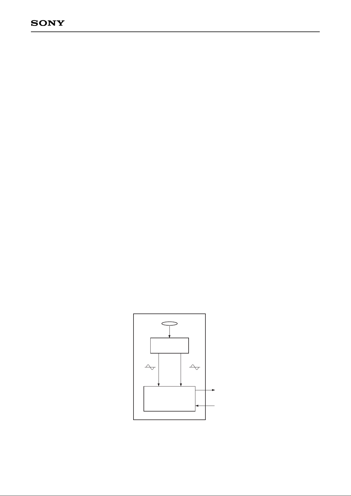
CXA1951AQ
RF Converter
CXD2931R
16ch GPS Processor
Antenna
TCXO
0V
IF
0V
RXD
TXD
GPS receiver system diagram using the CXD2931R
– 3 –
CXD2931R
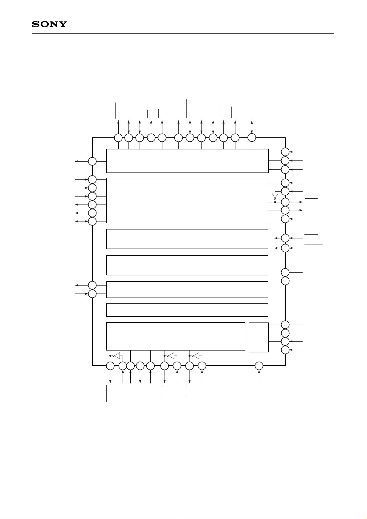
Block Diagram
ICS0, 1
IADR (0:18)
IB (0:15)
IRD
IWR
XCS0
DC0 to 5/PORT (16:21)
DADR (0:15)
DB (0:7)
DRD
DWR
PORT (0:15)
TEST0, 1
ICST0, 1
XROMW
EXRS
PWRST
VDD × 10
VSS × 10
AVD
AVS
VRT
VRB
CLKS
CLKI
CLKO
CLKOUT
TCXOS
NMI
HOLD
RXD0 to 2
PMI
TXD0 to 2
HOLDA
IODBK
SINT/PORT (22)
RUN
TOSEL
ITCXO
AVIN
OTCXO
TCXO
XTCXO
CCKI
CCKO
IF0
IF0O
36K Byte SRAM
UART (Baud Rate Generator) × 3
TIMER × 3
16ch GPS DSP
BIU
32bit RISC
256K Byte ROM
8bit
ADC
– 4 –
CXD2931R
Pin Configuration
1234567 8 9 10 11 12 13 14 15 16 17 18 19 20 21 22 23 24 25 26 27 28 29 30 31 32 33 34 35 36
37
38
39
40
41
42
43
44
45
46
47
48
49
50
51
52
53
54
55
56
57
58
59
60
61
62
63
64
65
66
67
68
69
70
71
72
133
134
135
136
137
138
139
140
141
142
143
144
121
122
123
124
125
126
127
128
129
130
131
132
109
110
111
112
113
114
115
116
117
118
119
120
DB6
DB7
SINT/PORT22
DCS0/PORT21
VDD
DCS1/PORT20
DCS2/PORT19
DCS3/PORT18
DCS4/PORT17
DCS5/PORT16
PORT15
PORT14
V
SS
PORT13
PORT12
PORT11
PORT10
PORT9
PORT8
PORT7
V
DD
PORT6
PORT5
PORT4
PORT3
PORT2
PORT1
PORT0
V
SS
TXD2
RXD2
TXD1
RXD1
TXD0
RXD0
V
DD
IB8
IB7
V
SS
IB6
IB5
IB4
IB3
IB2
IB1
V
DD
IB0
IADR18
IADR17
IADR16
IADR15
IADR14
IADR13
V
SS
IADR12
IADR11
IADR10
IADR9
IADR8
IADR7
IADR6
V
DD
IADR5
IADR4
IADR3
IADR2
IADR1
XROMW
ICS1
V
SS
ICS0
IRD
AVD
AVIN
VRT
VRB
AVS
V
SS
TCXO
XTCXO
V
DD
OTCXO
TEST0
TEST1
CCKI
CCKO
V
SS
ICST0
ICST1
IF0
IF0O
TCXOS
V
DD
HOLD
NMI
PMI
HOLDA
IODBK
EXRS
PWRST
V
SS
CLKI
CLKO
CLKS
CLKOUT
V
DD
RUN
IWR
73747576777879808182838485868788899096979899
100101102103104105106107108
9192939495
DB5
DB4
DB3
DB2
VSSDB1
DB0
DADR15
DADR14
DADR13
DADR12
DADR11
DADR10
VDDDADR9
DADR8
DADR7
DADR6
DADR5
DADR4
DADR3
DADR2
VSSDADR1
DADR0
XCS0
DWR
DRD
IB15
IB14
IB13
IB12
IB11
VDDIB10
IB9
– 5 –
CXD2931R
Pin
No.
1
2
3
4
5
6
7
8
9
10
11
12
13
14
15
16
17
18
19
20
21
22
23
24
25
26
27
28
29
30
31
32
33
34
35
AVD
AVIN
VRT
VRB
AVS
VSS
TCXO
XTCXO
VDD
OTCXO
TEST0
TEST1
CCKI
CCKO
VSS
ICST0
ICST1
IF0
IF0O
TCXOS
VDD
HOLD
NMI
PMI
HOLDA
IODBK
EXRS
PWRST
VSS
CLKI
CLKO
CLKS
CLKOUT
VDD
RUN
A/D converter power supply.
Analog input.
Reference input.
A/D converter GND.
GND
TCXO binary conversion circuit/crystal oscillator.
Power supply.
TCXO clock output.
Test. (Low level fixed)
Timer oscillation. (32.768kHz ± 100ppm)
GND
Test. (Low level fixed)
IF signal binary conversion circuit.
TCXO select. (Low: TCXO/2, High: TCXO through)
Power supply.
Hold input signal. (High: Hold)
Non maskable interrupt.
Program maskable interrupt.
Hold acknowledge signal.
Break signal for debugging.
Reset input signal.
Connect to main power supply. Leave open during backup.
GND
CPU clock oscillation circuit.
CPU clock select signal. (Low: TCXO, High: CLKI)
CPU clock output.
Power supply.
Signal indicating CPU operating status.
Symbol
—
I
I
I
—
—
I
O
—
O
I
I
I
O
—
I
I
I
O
I
—
I
I
I
O
O
I
I
—
I
O
I
O
—
O
I/O Description
Pin Configuration
– 6 –
CXD2931R
36
37
38
39
40
41
42
43
44
45
46
47
48
49
50
51
52
53
54
55
56
57
58
59
60
61
62
63
64
65
66
67
68
69
70
IWR
IRD
ICS0
VSS
ICS1
XROMW
IADR1
IADR2
IADR3
IADR4
IADR5
VDD
IADR6
IADR7
IADR8
IADR9
IADR10
IADR11
IADR12
VSS
IADR13
IADR14
IADR15
IADR16
IADR17
IADR18
IB0
VDD
IB1
IB2
IB3
IB4
IB5
IB6
VSS
Write signal for external expansion memory.
Read signal for external expansion memory.
Chip select 0 for external expansion memory.
GND
Chip select 1 for external expansion memory.
Wait signal for external expansion memory. (High: Wait)
(LSB)
Power supply.
GND
(MSB)
(LSB) Data bus I/O for external expansion memory.
Power supply.
GND
Address signal for external expansion memory.
Address signal for external expansion memory.
Address signal for external expansion memory.
Data bus I/O for external expansion memory.
O
O
O
—
O
I
I/O
I/O
I/O
I/O
I/O
—
I/O
I/O
I/O
I/O
I/O
I/O
I/O
—
I/O
I/O
I/O
I/O
I/O
I/O
I/O
—
I/O
I/O
I/O
I/O
I/O
I/O
—
Pin
No.
Symbol I/O Description
– 7 –
CXD2931R
71
72
73
74
75
76
77
78
79
80
81
82
83
84
85
86
87
88
89
90
91
92
93
94
95
96
97
98
99
100
101
102
103
104
IB7
IB8
IB9
IB10
VDD
IB11
IB12
IB13
IB14
IB15
DRD
DWR
XCS0
DADR0
DADR1
VSS
DADR2
DADR3
DADR4
DADR5
DADR6
DADR7
DADR8
DADR9
VDD
DADR10
DADR11
DADR12
DADR13
DADR14
DADR15
DB0
DB1
VSS
Power supply.
(MSB)
Read signal for external expansion data memory.
Write signal for external expansion data memory.
Chip select signal for external expansion data memory.
(LSB)
GND
Power supply.
(MSB)
(LSB)
GND
Data bus I/O for external expansion memory.
Data bus I/O for external expansion memory.
Address signal for external expansion data memory.
Address signal for external expansion data memory.
Address signal for external expansion data memory.
Data bus I/O for external expansion data memory.
I/O
I/O
I/O
I/O
—
I/O
I/O
I/O
I/O
I/O
O
O
O
I/O
I/O
—
I/O
I/O
I/O
I/O
I/O
I/O
I/O
I/O
—
I/O
I/O
I/O
I/O
I/O
I/O
I/O
I/O
—
Pin
No.
Symbol I/O Description
 Loading...