

Sony CXD2721Q-1 Datasheet

CXD2721Q-1
Single-Chip Digital Signal Processor for Karaoke
Description
The CXD2721Q-1 is a Karaoke LSI suitable for
use in video CD/LD/CD-G/CD and the like. A large
capacity DRAM and AD/DA converters are built in,
and a Karaoke mode providing simple surround and
Karaoke functions such as key control, microphone
echo and voice cancelling, and a music mode
providing functions such as surround, parametric
equalizer and bass/treble tone control are contained
on a single chip.
• Digital de-emphasis function
Features
• 3-channel 1-bit AD converter, decimation filter and
prefilter operational amplifier
S/N ratio: 92dB
THD + N: 0.02%
Filter pass band ripple: ±0.5dB or less
Filter stop band attenuation: –41dB or less
(all characteristics are typical values)
• 2-channel 1-bit DA converter, oversampling filter
and post filter
S/N ratio: 97dB
THD + N: 0.005%
Filter pass band ripple: ±0.2dB or less
Filter stop band attenuation: –41dB or less
(all characteristics are typical values)
• In addition to analog I/O, digital I/O (2-channel
input/2-channel output) are provided.
The interface also supports a wide variety of
formats.
• 128K-bit DRAM for key control, microphone echo
and surround processing
Functions
• Key controller pitch settings can be varied to a
maximum of ±1 octave with a precision of 14 bits.
• Microphone echo delay time can be varied to a
maximum of 278ms (when Fs = 44.1kHz).
• Voice canceller supports settings other than center
using panpot volumes.
• Voice parametric equalizer
• Voice pitch shifter
• Mixing function to support sound multiplexing
software
Sony reserves the right to change products and specifications without prior notice. This information does not convey any license by
any implication or otherwise under any patents or other right. Application circuits shown, if any, are typical examples illustrating the
operation of the devices. Sony cannot assume responsibility for any problems arising out of the use of these circuits.
• Simple surround function
• Music mode (switches with Karaoke mode)
Compressor function
Parametric equalizer function
Surround function
Bass/treble tone control function
Structure
Silicon gate CMOS
Applications
Equipment with Karaoke functions, such as video
CD/LD/CD-G/CD, compact music centers, video
games, etc.
Absolute Maximum Ratings (Ta = 25°C, VSS = 0V)
• Supply voltage VDD VSS – 0.5 to +7.0 V
• Input voltage VI VSS – 0.5 to VDD +0.5 V
• Output voltage VO VSS – 0.5 to VDD +0.5 V
• Operating temperature
• Storage temperature Tstg –55 to +150 °C
Recommended Operating Conditions
• Supply voltage VDD 4.5 to 5.25 (5.0 typ.) V
• Operating temperature
I/O Capacitance
• Input capacitance CIN 9 (max.) pF
• Output capacitance COUT 11 (max.) pF
• I/O capacitance CI/O 11 (max.) pF
∗
Measurement conditions: VDD = VI = 0V, F = 1MHz
100 pin QFP (Plastic)
Topr –20 to +75 °C
Ta –20 to +75 °C
– 1 –
E97110A72
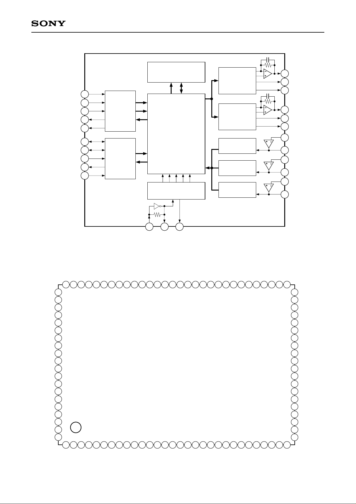
Block Diagram
CXD2721Q-1
RVDT
SCK
XLAT
REDY
TRDT
LRCK
BCK
SI
SO
XMST
98
99
100
94
93
92
91
95
128K bit DELAY RAM
DAC1
4
45
39
40
AOUT1
AO1N
AO1P
MICRO
29
33
34
AOUT2
AO2N
AO2P
1
COMPUTER
I/F
DAC2
DSP
AIN1
47
SERIAL
DATA
I/F
CLOCK GENERATOR
/TIMING CIRCUIT
37
36
14
ADC1
ADC2
ADC3
49
24
25
20
21
LO1
AIN2
LO2
AIN3
LO3
XTLI XTLO BFOT
Pin Configuration
TP
TP
80
79
81
TP
82
TP
83
SS6
V
84
DD5
V
85
TST0
86
TST1
87
TST2
88
TST3
89
SS7
V
90
XS24
91
SO
92
SI
93
BCK
94
LRCK
95
XMST
96
SS8
V
DD6
V
97
98
SCK
99
REDY
100
TRDT
1
2
NC
XLAT
78
TP
54
AVS2
3
SS
V
NC
53
28
2
DD
V
NC
NC
52
29
AOUT2
51
30
NC
50
49
48
47
46
45
44
43
42
41
40
39
38
37
36
35
34
33
32
31
AVS5
AVD1
LO1
NC
AIN1
AVS1
AOUT1
NC
AVS4
NC
AVD4
AO1P
AO1N
AVS6
XTLI
XTLO
AVD6
AO2P
AO2N
AVD5
NC
4
5
SS
DD
TP
75
76
77
6
5
4
3
NC
NC
RVDT
74
7
AVD0
TP
73
8
AVS0
TP
72
XRST
TP
V
V
TP
9
X768
71
10
TP
0
SS
V
70
11
TP
1
DD
V
69
12
TP
1
SS
V
68
13
TP
67
14
XWO
TP
66
15
BFOT
3
DD
V
65
16
BSL2
4
SS
V
64
17
BSL1
TP
2
SS
V
18
63
TP
1
DD
V
62
19
TP
61
20
AVS3
TP
60
21
AIN3
TP
LO3
59
22
TP
58
23
AVD3
TP
57
24
AVD2
TP
56
25
AIN2
TP
55
26 27
LO2
– 2 –
Pin Description
CXD2721Q-1
Pin
No.
1
2
3
4
5
6
7
8
9
10
11
12
13
14
15
Symbol I/O Description
XLAT
NC
NC
RVDT
NC
AVD0
AVS0
XRST
X768
VSS0
VDD1
VSS1
XWO
BFOT
BSL2
I
Latch input for microcomputer interface.
Open or fixed to Low.
Open or fixed to Low.
I
Data input for microcomputer interface.
Open or fixed to Low.
—
Digital power supply for built-in DRAM.
—
Digital GND for built-in DRAM.
I
System reset input. Reset when Low.
I
Test input pin. Normally fixed to Low.
—
Digital GND.
—
Digital power supply.
—
Digital GND.
I
Normally fixed to High.
O
Clock, frequency divider output. (384/768/256/512fs)
I
BFOT output clock frequency division ratio setting.
16
17
18
19
20
21
22
23
24
25
26
27
28
29
30
31
32
BSL1
VSS2
VDD1
AVS3
AIN3
LO3
AVD3
AVD2
AIN2
LO2
AVS2
NC
NC
AOUT2
AVS5
NC
AVD5
I
BFOT output clock frequency division ratio setting.
—
Digital GND.
—
Digital power supply.
—
CH3 AD converter GND.
I
CH3 AD converter analog input. (for microphone input)
O
CH3 AD converter LPF operational amplifier inverted output. (for microphone input)
—
CH3 AD converter power supply.
—
CH2 AD converter power supply.
I
CH2 AD converter analog input.
O
CH2 AD converter LPF operational amplifier inverted output.
—
CH2 AD converter GND.
Open or fixed to Low.
Open or fixed to Low.
O
CH2 DA converter LPF output.
—
CH2 DA converter GND.
Open or fixed to Low.
—
CH2 DA converter power supply.
33
34
35
AO2N
AO2P
AVD6
O
CH2 DA converter analog reversed phase output. (PWM)
O
CH2 DA converter analog forward phase output. (PWM)
—
Analog power supply for master clock.
– 3 –
CXD2721Q-1
Pin
No.
36
37
38
39
40
41
42
43
44
45
46
47
48
49
50
Symbol I/O Description
XTLO
XTLI
AVS6
AO1N
AO1P
AVD4
NC
AVS4
NC
AOUT1
AVS1
AIN1
NC
LO1
AVD1
O
Crystal oscillator circuit output.
I
Crystal oscillator circuit input.
—
Analog GND for master clock.
O
CH1 DA converter analog reversed phase output. (PWM)
O
CH1 DA converter analog forward phase output. (PWM)
—
CH1 DA converter power supply.
Open or fixed to Low.
—
CH1 DA converter GND.
Open or fixed to Low.
O
CH1 DA converter LPF output.
—
CH1 AD converter GND.
I
CH1 AD converter analog input.
Open or fixed to Low.
I
CH1 AD converter analog input. LPF operational amplifier inverted output.
—
CH1 AD converter power supply.
51
52
53
54
55
56
57
58
59
60
61
62
63
64
65
66
67
NC
NC
VDD2
VSS3
TP
TP
TP
TP
TP
TP
TP
TP
TP
TP
VSS4
VDD3
TP
Open or fixed to Low.
Open or fixed to Low.
—
Digital power supply.
—
Digital GND.
O
Test monitor pin. Normally Low output. Leave open.
O
Test monitor pin. Normally Low output. Leave open.
O
Test monitor pin. Normally Low output. Leave open.
O
Test monitor pin. Normally Low output. Leave open.
O
Test monitor pin. Normally Low output. Leave open.
O
Test monitor pin. Normally Low output. Leave open.
O
Test monitor pin. Normally Low output. Leave open.
O
Test monitor pin. Normally Low output. Leave open.
O
Test monitor pin. Normally Low output. Leave open.
O
Test monitor pin. Normally Low output. Leave open.
—
Digital GND.
—
Digital power supply.
O
Test monitor pin. Normally Low output. Leave open.
68
69
70
TP
TP
TP
O
Test monitor pin. Normally Low output. Leave open.
O
Test monitor pin. Normally Low output. Leave open.
O
Test monitor pin. Normally Low output. Leave open.
– 4 –
CXD2721Q-1
Pin
No.
71
72
73
74
75
76
77
78
79
80
81
82
83
84
85
Symbol I/O Description
TP
TP
TP
TP
TP
VSS5
VDD4
TP
TP
TP
TP
TP
VSS6
VDD5
TST0
O
Test monitor pin. Normally Low output. Leave open.
O
Test monitor pin. Normally Low output. Leave open.
O
Test monitor pin. Normally Low output. Leave open.
O
Test monitor pin. Normally Low output. Leave open.
O
Test monitor pin. Normally Low output. Leave open.
—
Digital GND.
—
Digital power supply.
O
Test monitor pin. Normally Low output. Leave open.
O
Test monitor pin. Normally Low output. Leave open.
O
Test monitor pin. Normally Low output. Leave open.
O
Test monitor pin. Normally Low output. Leave open.
O
Test monitor pin. Normally Low output. Leave open.
—
Digital GND.
—
Digital power supply.
I
Test pin. Normally fixed to Low.
86
87
88
89
90
91
92
93
94
95
96
97
98
99
100
TST1
TST2
TST3
VSS7
XS24
SO
SI
BCK
LRCK
XMST
VSS8
VDD6
SCK
REDY
TRDT
I
Test pin. Normally fixed to Low.
I
Test pin. Normally fixed to Low.
I
Test pin. Normally fixed to Low.
—
Digital GND.
I
Serial data 24-/32-bit slot selection. 24-bit slot when Low. (valid for slave mode)
O
1-sampling 2-channel serial data output.
I
1-sampling 2-channel serial data input.
I/O
Serial bit transfer clock for serial I/O data SI and SO.
I/O
Sampling frequency clock for serial I/O data SI and SO.
I
BCK, LRCK master/slave mode switching input. Master mode when Low.
—
Digital GND.
—
Digital power supply.
I
Shift clock input for microcomputer interface.
O
Transfer enabling signal output for microcomputer interface. Transfer prohibited when Low.
O
Serial data output for microcomputer interface.
– 5 –
CXD2721Q-1
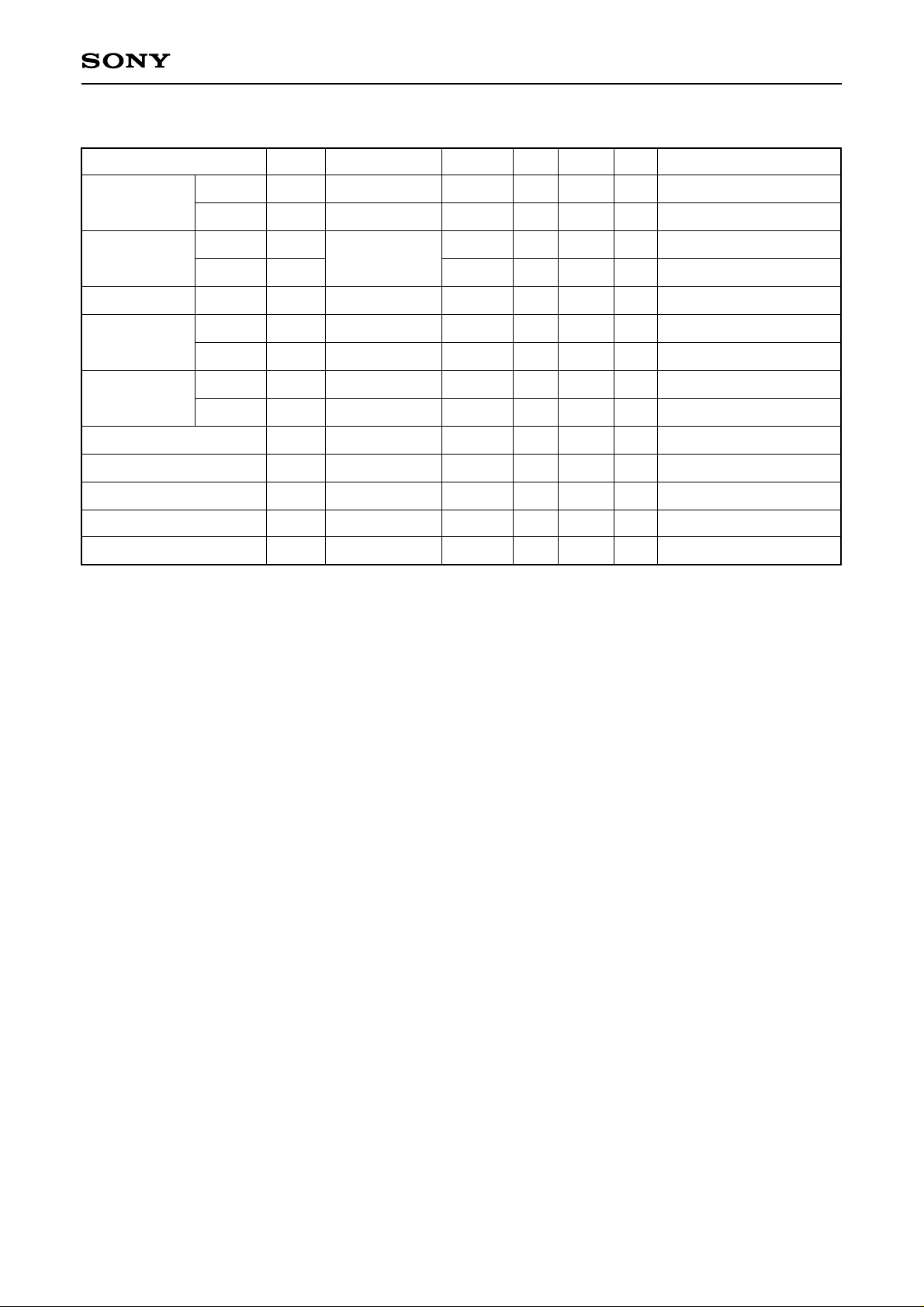
DC Characteristics (AVD0 to 6 = VDD0 to 6 = 4.5V to 5.25V, AVS0 to 6 = VSS0 to 8 = 0V, Ta = –20 to +75°C)
Item Symbol Conditions Min. Typ. Max. Unit Applicable pins
Input voltage (1)
High level
Low level
High level
Input voltage (2)
Low level
Input voltage (3)
Output voltage
(1)
Output voltage
(2)
High level
Low level
High level
Low level
Input leak current (1)
Input leak current (2)
Output leak current
Feedback resistance
VIH
VIL
VIH
VIL
VIN
VOH
VOL
VOH
VOL
II
II
IOZ
RFB
Schmitt input
Analog input
IOH = –2.0mA
IOL = 4.0mA
IOH = –12.0mA
IOL = 12.0mA
VIH = VDD, VSS
VIH = VDD, VSS
VIH = VDD, VSS
0.7VDD
0.8VDD
VSS
VDD – 0.8
VDD/2
–10
–40
–40
250k 1M
0.3VDD
0.2VDD
VDD
0.4
VDD/2
10
40
40
2.5M
∗1, ∗4, ∗5
V
∗1, ∗4, ∗5
V
∗3
V
∗3
V
∗2
V
∗6, ∗7, ∗8
V
∗6, ∗7, ∗8, ∗9
V
∗10
V
∗10
V
∗1, ∗3, ∗5
µA
∗4
µA
∗8, ∗9
µA
Ω
Resistance between ∗5and
∗10
Current consumption
∗1
XLAT, RVDT, X768, XWO, BSL2, BSL1, TST0 to TST3, XS24, SI, XMST, SCK
∗2
AIN1, AIN2, AIN3
∗3
XRST
∗4
During input to bidirectional pins BCK and LRCK
∗5
XTLI
∗6
During output from bidirectional pins BCK and LRCK
∗7
SO, BFOT
∗8
TRDT
∗9
REDY
∗10
XTLO
IDD
fS = 44.1kHz
125
132
mA
– 6 –
CXD2721Q-1
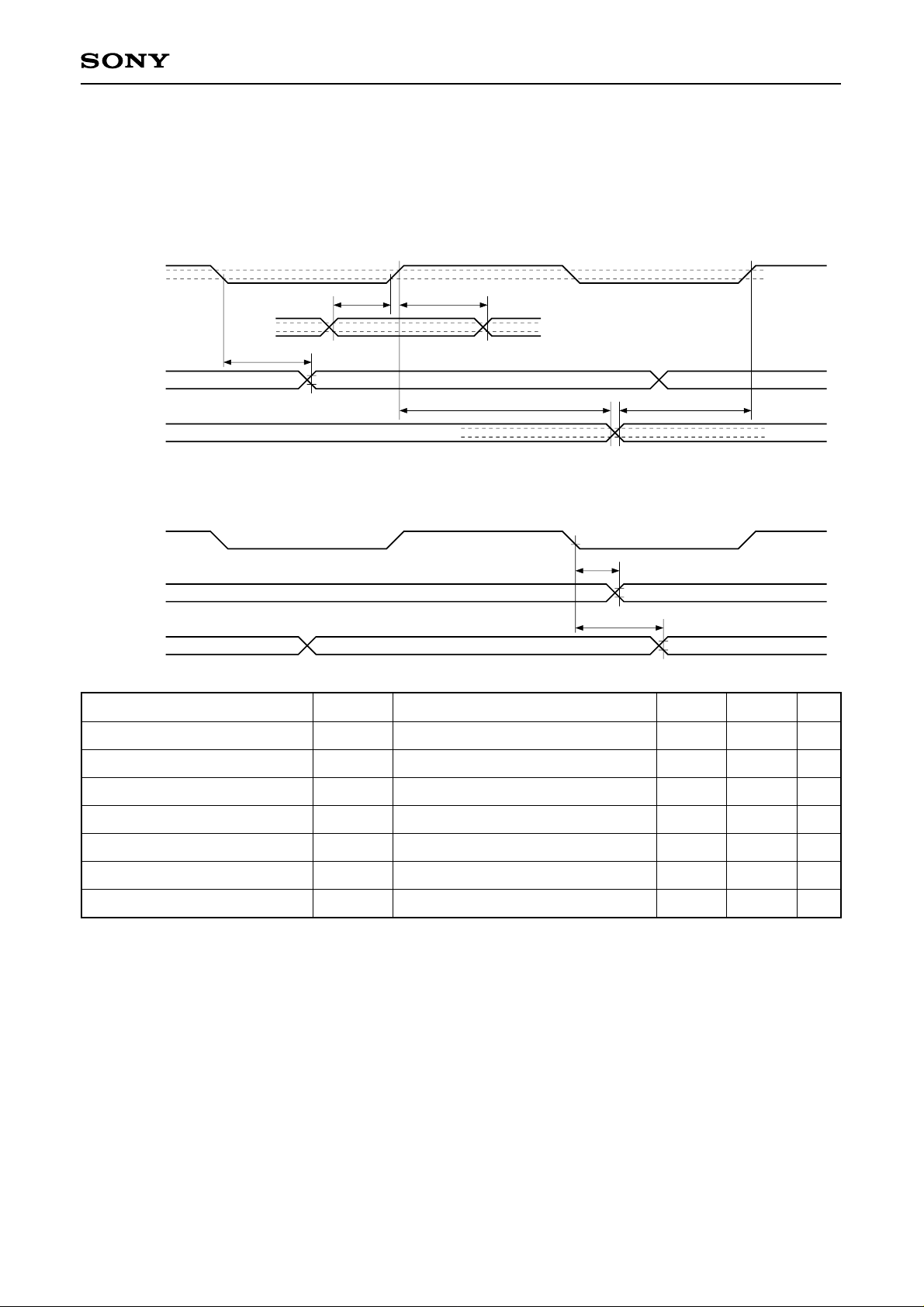
AC Characteristics (AVD0 to 6 = VDD0 to 6 = 4.5V to 5.25V, AVS0 to 6 = VSS0 to 8 = 0V, Ta = –20 to +75°C)
Serial Audio Interface Timing
[Slave mode]
BCK
SI
SO
LRCK
[Master mode]
BCK
LRCK
SO
Item
tDSSO
0.7VDD
0.3VDD
tHSItSSI
DD
0.7V
0.3VDD
tHLR
tDLR
tDMSO
tSLR
0.7VDD
0.3VDD
Symbol Conditions Min. Max. Unit
SI setup time
SI hold time
SO delay time
LRCK setup time
LRCK hold time
LRCK delay time
SO delay time
tSSI
tHSI
tDSSO
tSLR
tHLR
tDLR
tDMSO
Slave mode
Slave mode
Slave mode, CL = 60pF
Slave mode
Slave mode
Master mode, CL = 120pF
Master mode, CL = 60pF
20
40
20
40
50
50
100
ns
ns
ns
ns
ns
ns
ns
– 7 –
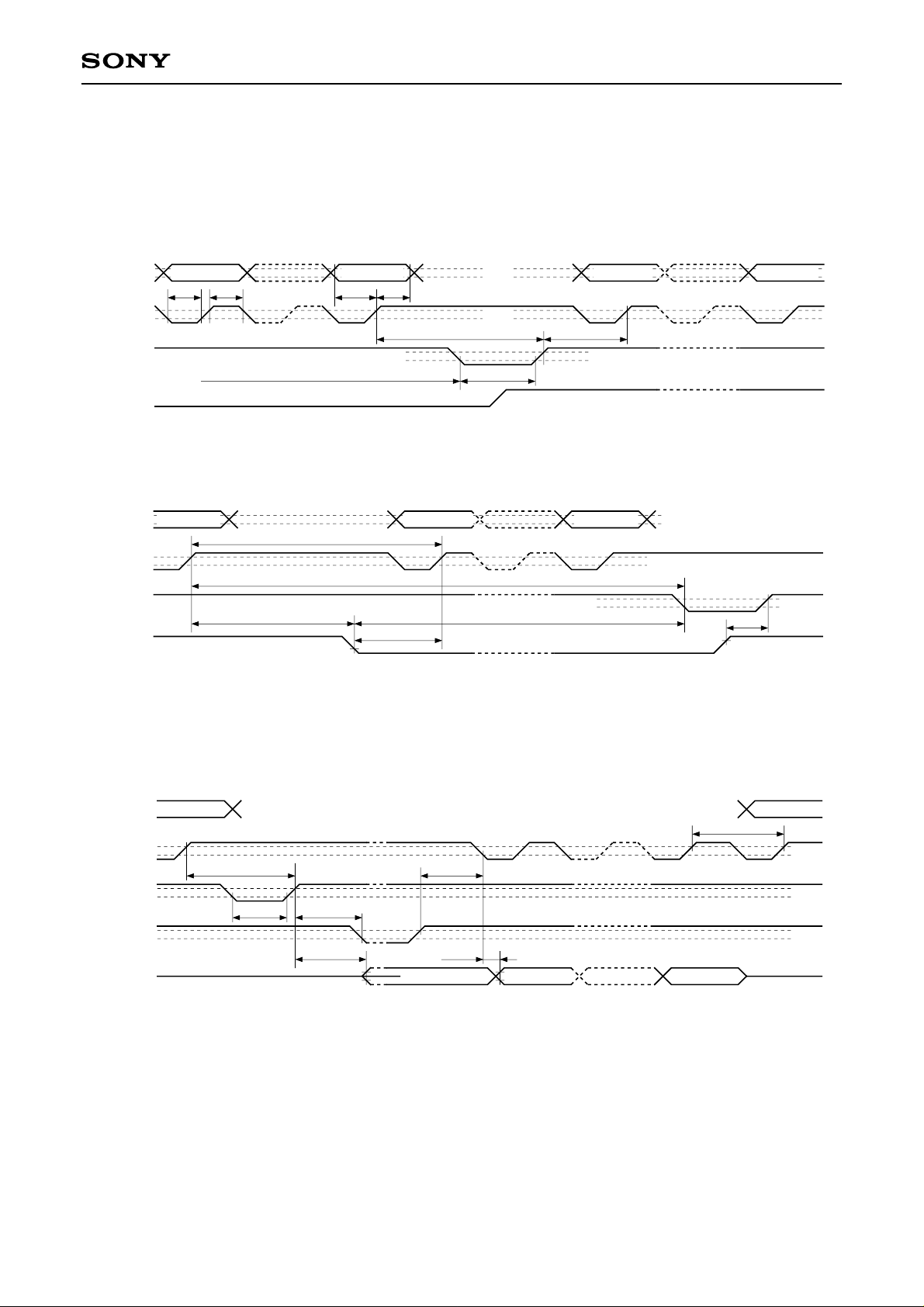
Microcomputer Interface Timing
[Write]
• Transfer timing for address section, transfer mode section and data section LSB
CXD2721Q-1
RVDT
SCK
Address LSB Data LSB Data MSB
tSWL
tSWH tDS tDH
Mode MSB
0.7VDD
0.3VDD
0.7VDD
0.3VDD
tLSDtSLP
XLAT
tLWH
tLWL
0.7VDD
0.3VDD
REDY
• Transfer timing from data section MSB to address section and transfer mode section
RVDT
SCK
XLAT
REDY
Data MSB Address LSB Mode MSB
tSS
tSLD
tSBD tLDR
tBSP
0.7VDD
0.3VDD
0.7VDD
0.3VDD
[Read]
tRLP
0.7VDD
0.3VDD
• Transfer timing for address section and transfer mode section is the same as for write.
RVDT
SCK
XLAT
REDY
TRDT
Mode MSB
tSLP
tLWL tLBD
tRSDP
tLDN tSDD
Data MSBData LSB
Address LSB
tSS
0.7VDD
0.3VDD
0.7VDD
0.3VDD
0.7VDD
0.3VDD
– 8 –
CXD2721Q-1
Item
RVDT setup time relative to SCK rise
RVDT data hold time from SCK rise
SCK Low level width
SCK High level width
XLAT Low level width
XLAT High level width
SCK rise preceding time relative to XLAT rise
SCK rise wait time relative to XLAT rise
Delay time to REDY fall relative to XLAT rise
Delay time to REDY fall relative to SCK rise
REDY fall preceding time relative to SCK rise
REDY rise preceding time relative to XLAT rise
REDY rise preceding time relative to SCK fall
XLAT fall wait time relative to SCK rise
XLAT fall delay time relative to REDY fall
Delay time from XLAT rise until TRDT data becomes active
Symbol Min.
tDS
tDH
tSWL
tSWH
tLWL
tLWH
1t + 20
1t + 20
1t + 20
1t + 20
1t + 20
tSLP
tLSD
3t + 20
tLBD
tSBD
tBSP
tRLP
tRSDP
tSLD
3t + 20
tLDR
tLDN
20
20
20
20
20
20
Max.
3t + 50
4t + 50
3t + 80
Unit
ns
ns
ns
ns
ns
ns
ns
ns
ns
ns
ns
ns
ns
ns
ns
ns
Delay time from SCK rise until TRDT data becomes high-impedance
Delay time from SCK fall until TRDT data is established
SCK rise wait time for next transfer
Note 1) t is the cycle of 2/3 the clock frequency applied to the XTLI pin. (512fs)
Note 2) REDY and TRDT pins are the values for CL = 60pF.
tSDF
tSDD
tSS
2t + 40
3t + 80
2t + 70
ns
ns
ns
– 9 –
CXD2721Q-1
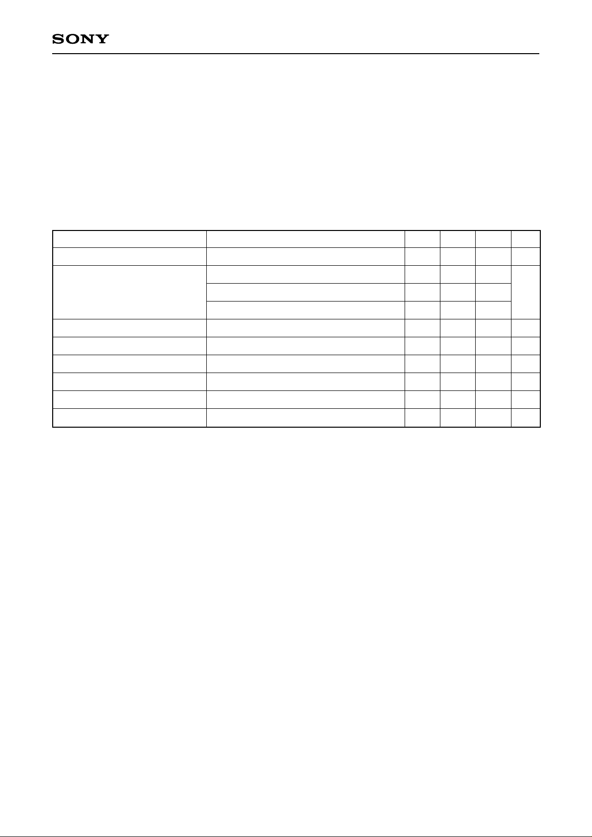
Analog Characteristics (AVD0 to 6 = VDD0 to 6 = 5.0V, AVS0 to 6 = VSS0 to 8 = 0.0V,
DSP: each function = OFF, gain = 1, Ta = 25°C)
1. ADC + DAC Connection Total Characteristics
Total characteristics using the measurement circuit in Fig. 1, including the prefilter with built-in operational
amplifier and the built-in post filter. Unless otherwise specified, the measurement conditions are as given
below.
• IN....0dB (= 2.0Vrms), 1kHz
• fs.....44.1kHz
S/N ratio
Item
EIAJ (with "A" weighting filter)
Measurement conditions Min. Typ. Max. Unit
EIAJ (0dB)
THD + N
∗1
EIAJ (–1dB)
EIAJ (–10dB)
Dynamic range
EIAJ
Channel separation
Level difference between channels
ADC input level
Output level
∗2
∗3
Analog current consumption
∗1
See Graph 1.
∗2
Input level to the ADC which outputs FS. (= prefilter output level)
∗3
Prefilter gain = –3.52dB
82 92
0.1
0.02
0.013
91
95
0.1
1.33
1.0
27
dB
%
0.03
dB
dB
dB
Vrms
Vrms
mA
– 10 –
CXD2721Q-1
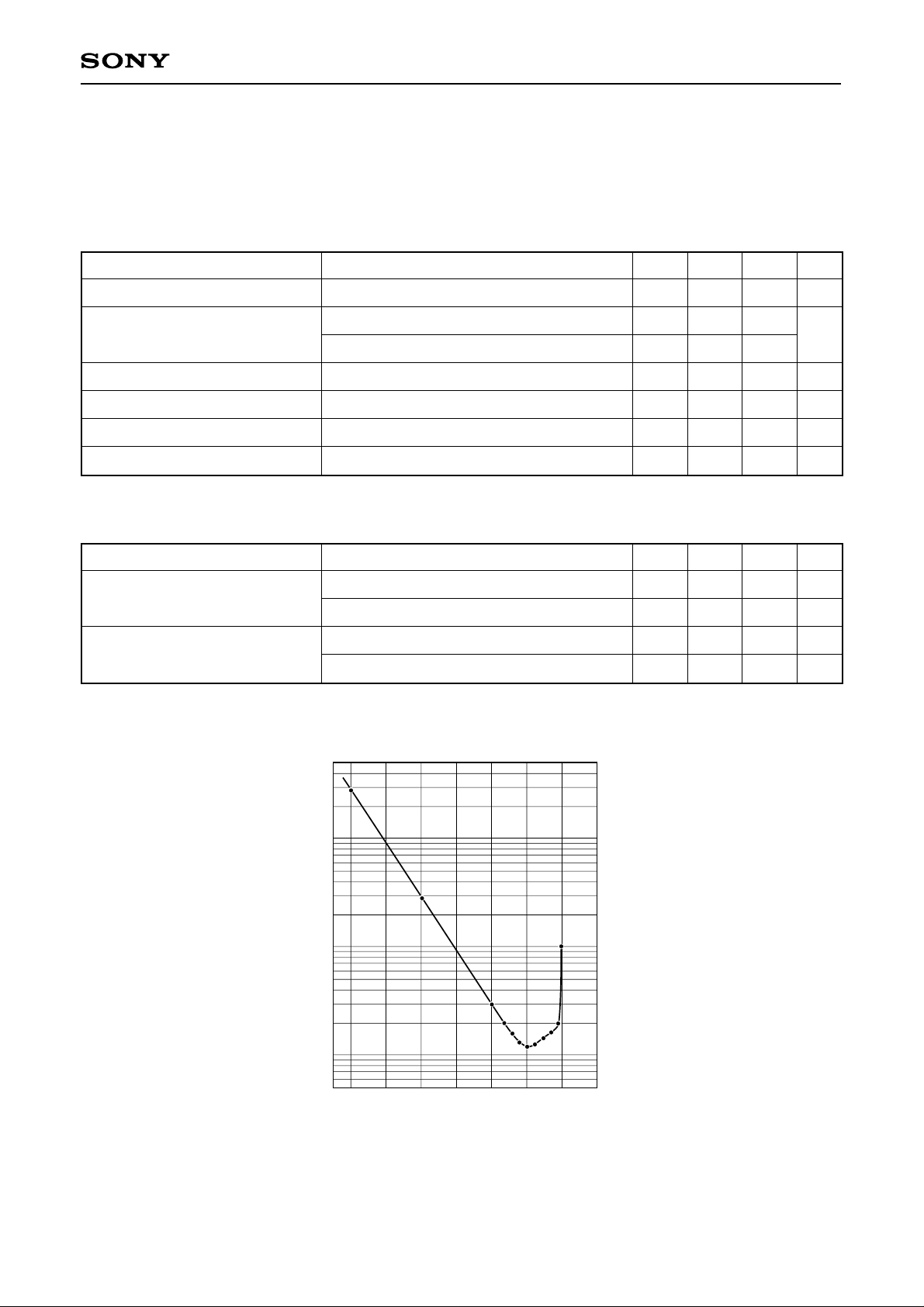
2. DAC Characteristics
Characteristics using the measurement circuit in Fig. 2, including the built-in post filter. Unless otherwise
specified, the measurement conditions are as given below.
• DATA....0dB (= FS), 1kHz, 16bit
• fs...........44.1kHz
Item
S/N ratio
THD + N
Dynamic range
Channel separation
Level difference between channels
Output level
3. Filter Characteristics
Block
Prefilter
Post filter
Measurement conditions Min. Typ. Max. Unit
EIAJ (with "A" weighting filter)
EIAJ (0dB)
EIAJ (–1dB)
EIAJ (–60dB)
EIAJ
EIAJ
EIAJ
Item
Feedback resistance value
Maximum amplification ratio (100kHz or less)
Load resistance value
Cut-off frequency (= fc)
Min.
10
10
97
dB
0.009
%
0.005
94
118
0.05
1.11
dB
dB
dB
Vrms
Typ. Max. Unit
kΩ
20
dB
kΩ
90
kHz
1.00
0.10
THD + N [%]
0.01
–60 –50 –40 –30 –20 –10 0 10
Analog input level [dB]
(2Vrms)
Graph 1.
– 11 –
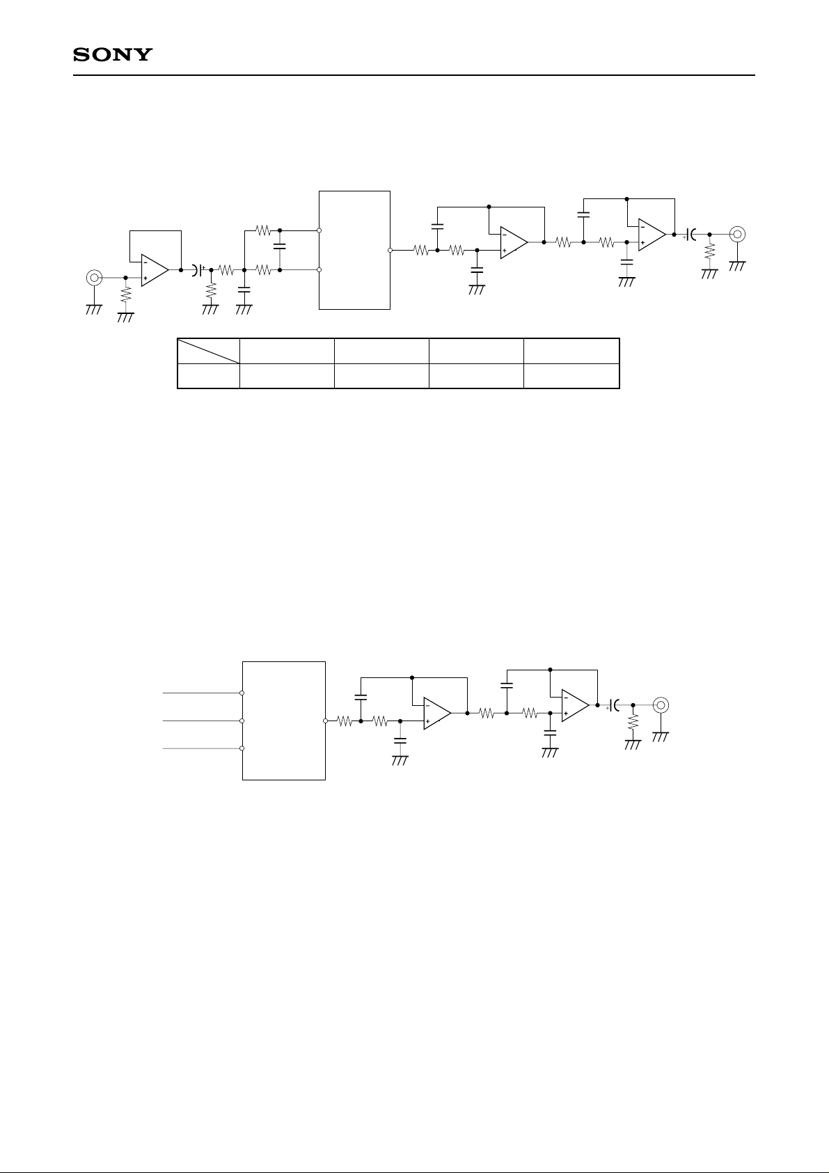
CXD2721Q-1
(Master mode)
CXD2721Q-1
22k
NE5532
IN
100k
10µ
33k
15k
CH
330p
AD1
R
R ∞ (= open)
100p
LOx
AOUTx
AINx
AD2
∞ (= open)
470p
NE5532 10µ
470p
AD3
1M
Unit
Ω
NE5532
10k10k
220p10k10k
330k
OUT1500p
Fig. 1. ADC + DAC Measurement Circuit
48fs
fs (= 44.1kHz)
DATA
CXD2721Q-1
(Slave mode)
BCK
LRCK
AOUTx
SI
470p
NE5532 10µ
470p
Fig. 2. DAC Measurement Circuit
NE5532
10k10k
220p10k10k
330k
OUT1500p
– 12 –
CXD2721Q-1
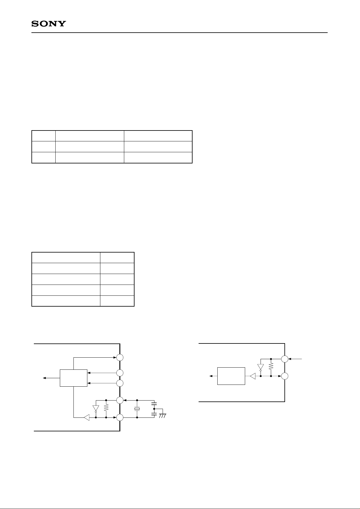
Description of Functions
1. Master/Slave Modes
[Relevant pins] XMST, LRCK, BCK
When connecting multiple CXD2721Q-1 or when using this LSI as a pair with a DA converter such as the
CXD2558M, one of the CXD2721Q-1 should be set to master mode to supply LRCK and BCK.
The clock applied to LRCK and BCK in slave mode must be synchronized to either the crystal oscillator clock
of the XTLI and XTLO pins or the external clock input from the XTLI pin.
XMST
H
L
Mode LRCK, BCK I/O
Slave mode
Master mode
Input
Output
Table 1-1. LRCK, BCK Mode Setting
2. Master Clock System
[Relevant pins] XTLI, XTLO, BFOT, BSL1, BSL2
768fs (fs = 44.1kHz) is assumed for the master clock system and the connection is as shown below. BFOT
outputs the clock obtained by frequency dividing the master clock. The frequency division ratio can be changed
by BSL1 and BSL2.
BSL2
0
0
1
1
BSL1
0
1
0
1
BFOT
384fs
768fs
256fs
512fs
(1) Master
512fs
Frequency
divider
BFOT
O
256fs/384fs/512fs/768fs
I
BSL1
I
BSL2
I
XTLI
O
768fs
XTLO
(2) Slave
Fig. 2-1.
– 13 –
512fs
Frequency
divider
I
O
768fs
XTLI
OPEN
XTLO
CXD2721Q-1
3. Reset Circuit
[Relevant pins] XRST, XTLI, XTLO
This LSI must be reset after the power is turned on.
Reset is performed by setting the XRST pin Low for 1/Fs or more after the supply voltage satisfies the
recommended operating condition, and the crystal oscillator clock of the XTLI and XTLO pins or the external
clock input from the XTLI pin is correctly applied.
4. Serial Audio Interface (SIF)
[Relevant pins] SI, SO, BCK, LRCK, XS24, XMST
Serial data is used for the external communication of the digital audio data.
The CXD2721Q-1 has one system each for input and output, and each system inputs/outputs 2 channels of
data per 1 sampling cycle. Either the 32-bit clock mode or the 24-bit clock mode can be selected. In master
mode, the setting is fixed to 32-bit clock mode.
(1) Pin Configuration
The pins shown in the table below are assigned to the SIF.
Symbol
SI
SO
BCK
LRCK
XS24
XMST
I/O Function
I
Serial input; taken synchronized to BCK.
O
Serial output; output synchronized to BCK.
I/O
I/O
BCK I/O; either 32-bit clock mode (64fs) or 24-bit clock mode (48fs). BCK output supports
32-bit clock mode only.
LRCK I/O (1fs).
SI0 slot number (24/32) selection input.
I
Low: 24-bit slot; High: 32-bit slot. Valid only in slave mode.
BCK, LRCK master mode/slave mode switching input.
I
Low: master mode; High: slave mode.
Table 4-1. Pin Configuration
– 14 –
CXD2721Q-1
(2) Operating Modes
LRCK/BCK mode and SI/SO system settings can be selected by the setup register settings as follows.
LRCK/BCK Mode Settings
Setup register
SQ11
SQ10
SQ09
LRCK format
LRCK polarity selection
BCK polarity selection relative to LRCK edge
SI/O System Register Settings
SI system
Setup register
SQ08
SQ07
SQ06
SQ05
SI data order
SI frontward/rearward truncation
SI data word length
SI data word length
Function Contents
"0": normal, "1": IIS
"0": Lch "H", "1": Lch "L"
"0": edge ↓, "1": edge ↑
Table 4-2. LRCK/BCK Mode Settings
Function Contents
"0": MSB first, "1": LSB first
"0": Frontward truncation, "1": Rearward truncation
SQ06 SQ05
0 0 : 16 bits
0 1 : 18 bits
1 0 : 20 bits
1 1 : 24 bits
Table 4-3. SI System Register Settings
SO system
Setup register
SQ04
SQ03
SQ02
SQ01
Function Contents
SO data order
SO frontward/rearward truncation
SO data word length
Table 4-4. SO System Register Settings
"0": MSB first, "1": LSB first
"0": Frontward truncation, "1": Rearward truncation
SQ02 SQ01
0 0 : 16 bits
0 1 : 18 bits
1 0 : 20 bits
1 1 : 24 bits
– 15 –
CXD2721Q-1
(3) SIF Format
The serial interface has one input/output system each, and except for the slot number, the following formats
can be set independently for the input and output systems by setting the setup register. The serial interface
can also be made to support IIS format, to enable connection to Philips and other devices. The timing charts
for each data format are shown on pages 18 and 19.
32-bit slot (XS24 = High)
Setup register
SI format
MSB first 16 bits Frontward truncation
MSB first 18 bits Frontward truncation
MSB first 20 bits Frontward truncation
MSB first 24 bits Frontward truncation
MSB first 16 bits Rearward truncation
LSB first 16 bits Rearward truncation
LSB first 18 bits Rearward truncation
LSB first 20 bits Rearward truncation
LSB first 24 bits Rearward truncation
Table 4-5. 32-bit Slot Serial IN
Setup register
SO format
MSB first 16 bits Rearward truncation
MSB first 18 bits Rearward truncation
MSB first 20 bits Rearward truncation
MSB first 24 bits Rearward truncation
MSB first 24 bits Frontward truncation
LSB first 24 bits Rearward truncation
SQ05 SQ06 SQ07
0
0
0
1
0
0
0
1
0
1
1
0
0
0
1
0
0
1
1
0
1
0
1
1
1
1
1
SQ01 SQ02 SQ03
0
0
1
1
0
1
0
1
1
1
1
1
1
1
0
1
1
1
SQ08
0
0
0
0
0
1
1
1
1
SQ04
0
0
0
0
0
1
Table 4-6. 32-bit Slot Serial OUT
– 16 –
24-bit slot (XS24 = Low)
CXD2721Q-1
Setup register
SI format
MSB first 16 bits Rearward truncation
MSB first 16 bits Frontward truncation
MSB first 18 bits Frontward truncation
MSB first 20 bits Frontward truncation
MSB first 24 bits
LSB first 16 bits Rearward truncation
LSB first 18 bits Rearward truncation
LSB first 20 bits Rearward truncation
LSB first 24 bits
Table 4-7. 24-bit Slot Serial IN
Setup register
SO format
MSB first 16 bits Rearward truncation
MSB first 18 bits Rearward truncation
MSB first 20 bits Rearward truncation
MSB first 24 bits
LSB first 24 bits
SQ05 SQ06 SQ07
0
0
1
0
0
0
1
0
0
0
1
0
1
1
0
0
0
1
1
0
1
0
1
1
1
1
1
SQ01 SQ02 SQ03
0
0
1
1
0
1
0
1
1
1
1
∗
1
1
∗
SQ08
0
0
0
0
0
1
1
1
1
SQ04
0
0
0
0
1
Table 4-8. 24-bit Slot Serial OUT
Note) ∗ means "don't care".
– 17 –
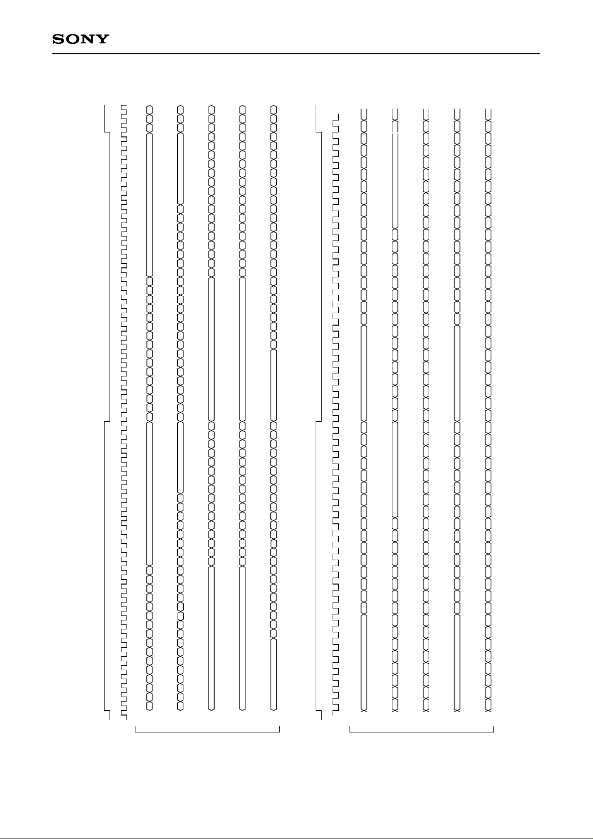
LSBMSB
CXD2721Q-1
MSB
Invalid
Rch
14 13 12 11 10 09 08 07 06 05 04 03 02 01 0015
Invalid Invalid
Invalid Invalid
LSBMSB
15 14 13 12 11 10 09 08 07 06 05 04 03 02 01 00
Invalid
LSBMSB LSBMSB
Invalid
LSB
MSBLSB
00 01 02 03 04 05 06 07 08 09 10 11 12 13 14 15 16 17 18 19 20 21 22 2300 01 02 03 04 05 06 07 08 09 10 11 12 13 14 15 16 17 18 19 20 21 22 23
Invalid
LSB MSB
Rch
14 13 12 11 10 09 08 07 06 05 04 03 02 01 0015
Invalid
LSBMSB LSBMSB
14 13 12 11 10 09 08 07 06 05 04 03 02 01 0015
MSB LSB MSB
Fig. 4-1.
Invalid
LSBMSB LSBMSB
Lch
LRCK
32bit slot
15 14 13 12 11 10 09 08 07 06 05 04 03 02 01 00
LSB MSB LSB
Invalid
14 13 12 11 10 09 08 07 06 05 04 03 02 01 0015
• MSB first 16 bits frontward truncation
BCK
23 22 21 20 19 18 17 16 15 14 13 12 11 10 09 08 07 06 05 04 03 02 01 00 23 22 21 20 19 18 17 16 15 14 13 12 11 10 09 08 07 06 05 04 03 02 01 00
MSB
• MSB first 24 bits frontward truncation
• MSB first 16 bits rearward truncation
SI
00 01 02 03 04 05 06 07 08 09 10 11 12 13 14 15 00 01 02 03 04 05 06 07 08 09 10 11 12 13 14 15
Invalid
• LSB first 16 bits rearward truncation
LSB MSB
Invalid
• LSB first 24 bits rearward truncation
Lch
LRCK
• MSB first 16 bits rearward truncation
BCK
24bit slot
14 13 12 11 10 09 08 07 06 05 04 03 02 01 0015
Invalid
14 13 12 11 10 09 08 07 06 05 04 03 02 01 0015
• MSB first 16 bits frontward truncation
• MSB first 24 bits
Digital Audio Data Input Timing (with polarities: SQ11 = 0, SQ10 = 0, SQ09 = 0)
– 18 –
00 01 02 03 04 05 06 07 08 09 10 11 12 13 14 15 00 01 02 03 04 05 06 07 08 09 10 11 12 13 14 15
Invalid Invalid
23 22 21 20 19 18 17 16 15 14 13 12 11 10 09 08 07 06 05 04 03 02 01 00 23 22 21 20 19 18 17 16 15 14 13 12 11 10 09 08 07 06 05 04 03 02 01 00
MSB LSB MSB LSB
• LSB first 16 bits rearward truncation
00 01 02 03 04 05 06 07 08 09 10 11 12 13 14 15 16 17 18 19 20 21 22 23 00 01 02 03 04 05 06 07 08 09 10 11 12 13 14 15 16 17 18 19 20 21 22 23
LSB MSB LSB MSB
• LSB first 24 bits
SI
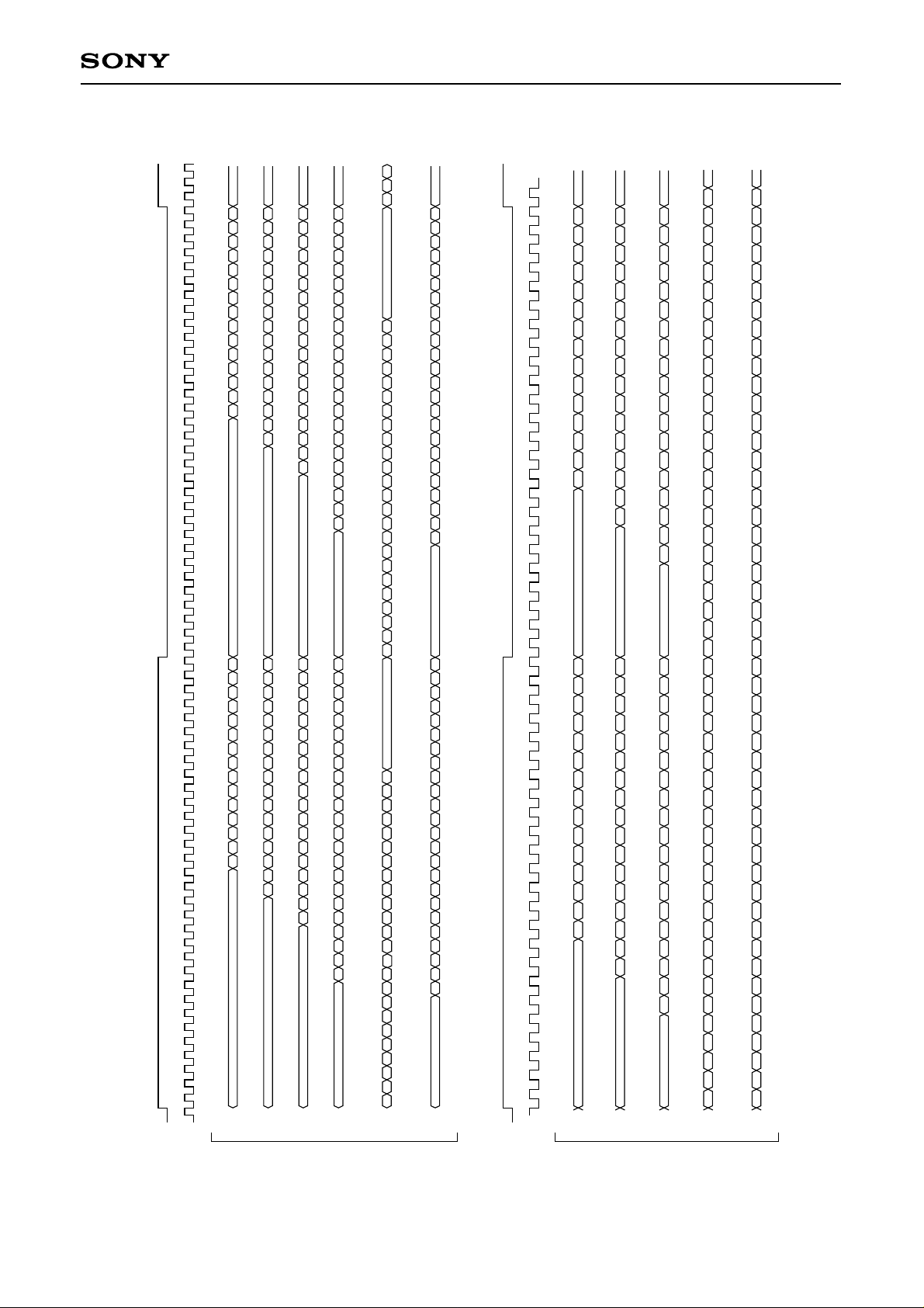
CXD2721Q-1
Rch
LSBMSB
LSBMSB
LSBMSB
LSBMSB
MSBLSB
" 0 " truncation" 0 " truncation
LSBMSB
14 13 12 11 10 09 08 07 06 05 04 03 02 01 00
Rch
16 15 14 13 12 11 10 09 08 07 06 05 04 03 02 01 00
18 17 16 15 14 13 12 11 10 09 08 07 06 05 04 03 02 01 00
15
17
22 21 20 19 18 17 16 15 14 13 12 11 10 09 08 07 06 05 04 03 02 01 00
00 01 02 03 04 05 06 07 08 09 10 11 12 13 14 15 16 17 18 19 20 21 22 23
19
23
" 0 " truncation
14 13 12 11 10 09 08 07 06 05 04 03 02 01 00
MSB
16 15 14 13 12 11 10 09 08 07 06 05 04 03 02 01 00
18 17 16 15 14 13 12 11 10 09 08 07 06 05 04 03 02 01 00
15
17
19
Lch
LRCK
32bit slot
LSB
LSB
14 13 12 11 10 09 08 07 06 05 04 03 02 01 00
16 15 14 13 12 11 10 09 08 07 06 05 04 03 02 01 00
MSB
18 17 16 15 14 13 12 11 10 09 08 07 06 05 04 03 02 01 00
MSB
LSB
LSB
MSB
22 21 20 19 18 17 16 15 14 13 12 11 10 09 08 07 06 05 04 03 02 01 00
15
17
19
• MSB first 16 bits rearward truncation
• MSB first 20 bits rearward truncation
• MSB first 18 bits rearward truncation
BCK
MSB
23
• MSB first 24 bits rearward truncation
SO
MSBLSB
LSB
Lch
00 01 02 03 04 05 06 07 08 09 10 11 12 13 14 15 16 17 18 19 20 21 22 23
" 0 " truncation
23 22 21 20 19 18 17 16 15 14 13 12 11 10 09 08 07 06 05 04 03 02 01 00 23 22 21 20 19 18 17 16 15 14 13 12 11 10 09 08 07 06 05 04 03 02 01 00
MSB
• MSB first 24 bits frontward truncation
• LSB first 24 bits rearward truncation
LRCK
• MSB first 16 bits rearward truncation
BCK
24bit slot
LSB LSB
14 13 12 11 10 09 08 07 06 05 04 03 02 01 00
MSB
16 15 14 13 12 11 10 09 08 07 06 05 04 03 02 01 00
MSB
15
• MSB first 18 bits rearward truncation
18 17 16 15 14 13 12 11 10 09 08 07 06 05 04 03 02 01 00
17
19
• MSB first 20 bits rearward truncation
LSB MSB LSB
MSB
23 22 21 20 19 18 17 16 15 14 13 12 11 10 09 08 07 06 05 04 03 02 01 00 23 22 21 20 19 18 17 16 15 14 13 12 11 10 09 08 07 06 05 04 03 02 01 00
MSB
• MSB first 24 bits
• LSB first 24 bits
LSB MSB LSB
LSB MSB LSB
SO
Fig. 4-2.
00 01 02 03 04 05 06 07 08 09 10 11 12 13 14 15 16 17 18 19 20 21 22 23 00 01 02 03 04 05 06 07 08 09 10 11 12 13 14 15 16 17 18 19 20 21 22 23
LSB MSB LSB MSB
Digital Audio Data Output Timing (with polarities: SQ11 = 0, SQ10 = 0, SQ09 = 0)
– 19 –
CXD2721Q-1
5. Microcomputer Interface
[Relevant pins] RVDT, TRDT, SCK, XLAT, REDY
The CXD2721Q-1 performs the serial audio interface format setting and coefficient settings such as volume
and microphone echo delay amount by serial data from the microcomputer.
Further, bidirectional communication such as internal data read from the CXD2721Q-1 to the microcomputer
can be performed at the rate of once per 1 LRCK.
(1) Pin Configuration
The five external pins indicated in the table below are assigned to the microcomputer interface.
The microcomputer interface begins operation when XLAT is received, so multiple CXD2721Q-1 can be used
by connecting RVDT, TRDT, SCK and REDY in common and controlling (wiring) only XLAT separately.
Symbol
RVDT
TRDT
SCK
XLAT
REDY
I/O Function
I
Serial data input from microcomputer.
Serial data output to the microcomputer. High impedance status unless this pin is set to
O
internal data read status by the microcomputer. Therefore, pull-up or pull-down should be
performed so that the potential is not unstable when this pin is not active.
Shift clock for serial data. Input data from RVDT is taken according to the SCK rise, and
I
output data from TRDT is sent out according to the SCK fall.
Interprets the 8 bits of RVDT before this signal rises as transfer mode data, and the bits
I
before that as address data.
Transfer prohibited when Low level. Transfer enabled when High. This pin is an open drain,
O
and must be pulled up externally.
Table 5-1. Microcomputer Interface External Pins
– 20 –
CXD2721Q-1
(2) Description of Communication Formats
The data transfer timing between the microcomputer interface and the coefficient RAM and setup register is
called the SV cycle, and is generated once per 1 LRCK.
The SV cycle is generated immediately preceding the signal processing program, so it has absolutely no effect
on signal processing, and there is no risk of the sound being cut.
In read/write modes,
Address section + Mode section + Data section
act as one package of data to perform data transfer between the microcomputer and the CXD2721Q-1.
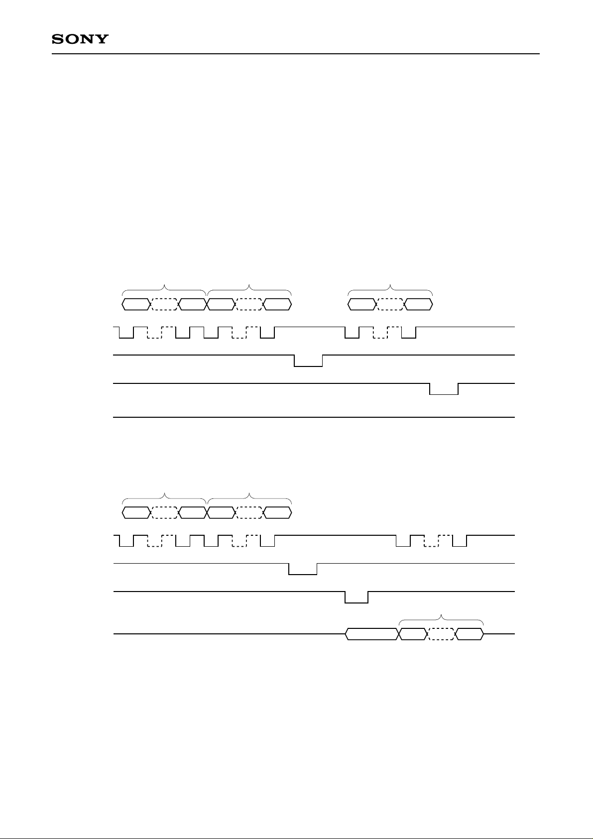
[Write] • For coefficient RAM
Address section (8 bits) Mode section (8 bits) Data section (16 bits)
RVDT
SCK
XLAT
REDY
TRDT
A0 A7 M0 M7 D0 D15
[Read] • For coefficient RAM
Address section (8 bits) Mode section (8 bits)
RVDT
SCK
XLAT
A0 A7 M0 M7
REDY
TRDT
Note) For both read and write, the data section is 24 bits for the setup register.
Fig. 5-1. Examples of Communication
– 21 –
Data section (16 bits)
D0 D15
 Loading...