

Sony CXD2720Q-2 Datasheet

– 1 –
CXD2720Q-2
E97315-PS
Single-Chip Digital Signal Processor for Karaoke
Description
The CXD2720Q-2 is a digital signal processor LSI
for Karaoke, suitable for use in LD/CD/CD-G/video
CD and the like.
A large capacity DRAM and AD/DA converters are
built in, and Karaoke functions such as key control
and microphone echo are contained on a single
chip.
Features
• 3-channel 1-bit AD converter and decimation filter
S/N ratio: 88 dB
THD + N: 0.016%
Filter pass band ripple: less than ±0.008dB
Filter stop band attenuation: less than –62dB
(all characteristics are typical values)
• 2-channel 1-bit DA converter and oversampling
filter
S/N ratio: 98dB
THD + N: 0.006%
Filter pass band ripple: less than ±0.2dB
Filter stop band attenuation: less than –41dB
(all characteristics are typical values)
• In addition to analog input/output, 2-channel input/
2-channel output of digital input/output are provided.
The interface also supports a variety of formats.
• 128K-bit DRAM for key control and microphone
echo processing
Functions
• Key controller pitch setting can be varied to a
maximum of ±1 octave with a precision of 14 bits
• Two key controllers are provided.
For their pitches, either of common or independent
setting is possible
• Key controller can be used for voice
• Microphone echo delay time can be varied to a
maximum of 185ms (when fs = 44.1kHz)
• Voice parametric equalizer
• Mixing function to support sound multiplexing
software
• Digital de-emphasis function
• Soft mute function
Structure
Silicon gate CMOS
Applications
Equipment having Karaoke function, such as
LD/CD, compact music center, video games, etc.
Absolute Maximum Ratings
(Ta = 25°C, VSS = 0V)
• Supply voltage VDD VSS – 0.5 to +7.0 V
• Input voltage VI VSS – 0.5 to VDD + 0.5 V
• Output voltage VO VSS – 0.5 to VDD + 0.5 V
• Operating temperature
Topr –20 to +75 °C
• Storage temperature Tstg –55 to +150 °C
Recommended Operating Conditions
• Supply voltage VDD 4.5 to 5.5 (5.0 typ.) V
• Operating temperature
Ta –20 to +75 °C
Input/Output Capacitance
• Input capacitance CIN 9 (max.) pF
• Output capacitance COUT 11 (max.) pF
• Input/output capacitance CI/O 11 (max.) pF
∗
Measurement conditions: VDD = VI = 0V, F = 1MHz
Sony reserves the right to change products and specifications without prior notice. This information does not convey any license by
any implication or otherwise under any patents or other right. Application circuits shown, if any, are typical examples illustrating the
operation of the devices. Sony cannot assume responsibility for any problems arising out of the use of these circuits.
100 pin QFP (Plastic)

– 2 –
CXD2720Q-2
3
4
5
6
7
25
26
40
39
32
33
82
128K bit DELAY RAM
DSP
CLOCK GENERATOR
/TIMING CIRCUIT
DAC1
DAC2
ADC1
ADC2
ADC3
29
22
36
MICRO
COMPUTER
I/F
SERIAL
DATA
I/F
8
12
88
87
86
AIN1
RVDT
SCK
XLAT
REDY
TRDT
LRCK
BCK
SI
SO
XWO
XTLI XTLO BFOT
AO1P
AO1N
AO2N
AO2P
AIN2
AIN3
Block Diagram
40
39
38
37
36
35
34
31
32
33
41
42
43
44
45
46
47
48
49
50
51
52
53
54
55
56
57
58
59
60
70
69
68
67
63
64
65
66
61
62
71
72
73
74
75
7677
78
79
80
81
82
83
84
88
87
86
85
89
90
100
99
98
97
96
95
94
91
92
93
2
3
4
5
6
7
8
9
10
11
12
13
14
15
16
17
18
19
20
21
22
23
24
25
26 27
28
29
30
1
AV
S
0
V
SS
0
RVDT
SCK
XLAT
REDY
TRDT
XWO
XRST
V
SS
1
V
DD
0
SO
XS24
TST0
TST1
TST2
TST3
TST4
TST5
V
SS
2
AV
S
3
AIN3
AV
D
3
AV
D
4
AO1P
AO1N
AV
S
4
AV
S
1
AIN1
AV
D
1
V
SS
6
NC
NC
NC
NC
NC
NC
NC
NC
NC
V
DD
2
V
SS
5
NC
NC
NC
NC
NC
NC
NC
NC
NC
NC
NC
NC
NC
NC
NC
V
SS
4
NC
NC
NC
NC
NC
NC
NC
NC
NC
V
DD1
V
SS3
AV
S5
AO2P
AO2N
AV
D5
AV
D2
AIN2
AV
S2
XV
SS
XTLI
XTLO
XV
DD
LRCK
X768
BFOT
INVI
NC
NC
SI
BCK
XMST
V
SS7
NC
NC
NC
NC
NC
NC
NC
NC
V
DD3
AV
D0
Pin Configuration

– 3 –
CXD2720Q-2
Pin Description
Pin
No.
1
2
3
4
5
6
7
8
9
10
11
12
13
14
15
16
17
18
19
20
21
22
23
24
25
26
27
28
29
30
31
32
33
34
35
AVS0
VSS0
RVDT
SCK
XLAT
REDY
TRDT
XWO
XRST
VSS1
VDD0
SO
XS24
TST0
TST1
TST2
TST3
TST4
TST5
VSS2
AVS3
AIN3
AVD3
AVD4
AO1P
AO1N
AVS4
AVS1
AIN1
AVD1
XVDD
XTLO
XTLI
XVSS
AVS2
—
—
I
I
I
O
O
I
I
—
—
O
I
I
I
I
I
I
I
—
—
I
—
—
O
O
—
—
I
—
—
O
I
—
—
DRAM digital GND.
Digital GND.
Data input for microcomputer interface.
Shift clock input for microcomputer interface.
Latch input for microcomputer interface.
Transmission enabling signal output for microcomputer interface. Transmission
prohibited when Low.
Serial data output for microcomputer interface.
Window open input for synchronization. Normally High.
System reset input. Resets when Low.
Digital GND.
Digital power supply.
1-sampling 2-channel serial data output.
Serial data 24-/32-bit slot selection. 24-bit slot when Low. (valid for slave mode)
Test pin. Normally set Low.
Test pin. Normally set Low.
Test pin. Normally set Low.
Test pin. Normally set Low.
Test pin. Normally set Low.
Test pin. Normally set Low.
Digital GND.
CH3 AD converter GND.
CH3 AD converter analog input (for microphone input).
CH3 AD converter power supply.
CH1 DA converter power supply.
CH1 DA converter analog positive phase output.
CH1 DA converter analog reversed phase output.
CH1 DA converter GND.
CH1 AD converter GND.
CH1 AD converter analog input.
CH1 AD converter power supply.
Digital power supply for master clock.
Crystal oscillator circuit output.
Crystal oscillator circuit input.
Digital GND for master clock.
CH2 AD converter GND.
Symbol I/O Description
– 4 –
CXD2720Q-2
Pin
No.
36
37
38
39
40
41
42
43
44 to 52
53
54 to 68
69
70
71 to 79
80
81
82
83
84
85
86
87
88
89
90
91 to 98
99
100
AIN2
AVD2
AVD5
AO2N
AO2P
AVS5
VSS3
VDD1
NC
VSS4
NC
VSS5
VDD2
NC
VSS6
X768
BFOT
INVI
NC
NC
SI
BCK
LRCK
XMST
VSS7
NC
VDD3
AVD0
I
—
—
O
O
—
—
—
—
—
—
—
I
O
I
I
I/O
I/O
I
—
—
—
CH2 AD converter analog input.
CH2 AD converter power supply.
CH2 DA converter power supply.
CH2 DA converter analog reversed phase output.
CH2 DA converter analog positive phase output.
CH2 DA converter GND.
Digital GND.
Digital power supply.
Normally open.
Digital GND.
Normally open.
Digital GND.
Digital power supply.
Normally open.
Digital GND.
Test input pin. Normally set Low.
Clock, frequency-divider output (384fs).
Test pin. Normally set Low.
Normally open.
Normally open.
1-sampling 2-channel serial data input.
Serial bit transmission clock for serial input/output data SI and SO.
Sampling frequency clock for serial input/output data SI and SO.
BCK, LRCK master/slave mode switching input. Master mode when Low.
Digital GND.
Normally open.
Digital power supply.
Digital power supply for DRAM.
Symbol I/O Description

– 5 –
CXD2720Q-2
DC Characteristics
(AVD0 to 5 = XVDD = VDD0 to 3 = 5V ± 10%, AVS0 to 5 = XVSS = VSS0 to 7 = 0V, Ta = –20 to +75°C)
Item Symbol Conditions Min. Typ. Max. Unit Applicable pins
High level
Low level
High level
Low level
High level
Low level
High level
Low level
High level
Low level
VIH
VIL
VIH
VIL
VIN
VOH
VOL
VOH
VOL
VOH
VOL
II
II
IOZ
RFB
IDD
Analog input
IOH = –2.0mA
IOL = 4.0mA
IOH = –6.0mA
IOL = 4.0mA
IOH = –12.0mA
IOL = 12.0mA
VIH = VDD, VSS
VIH = VDD, VSS
VIH = VDD, VSS
fs = 44.1kHz
0.7VDD
0.8VDD
VSS
VDD – 0.8
VDD – 0.8
VDD/2
–10
–40
–40
250k
1M
79
0.3VDD
0.2VDD
VDD
0.4
0.4
VDD/2
10
40
40
2.5M
90
V
V
V
V
V
V
V
V
V
V
V
µA
µA
µA
Ω
mA
∗1, ∗4, ∗5
∗1, ∗4, ∗5
∗3
∗3
∗2
∗6, ∗7, ∗8
∗6, ∗7, ∗8, ∗9
∗10
∗10
∗11
∗11
∗1, ∗3, ∗5
∗4
∗8, ∗9
Resistance
between
∗5
and ∗11.
Input voltage (1)
Input voltage (2)
Output voltage
(1)
Output voltage
(2)
Output voltage
(3)
Input leak current (1)
Input leak current (2)
Output leak current
Feedback resistance
Current consumption
Input voltage (3)
∗1
RVDT, SCK, XLAT, XWO, XRST, XS24, TST0 to TST5, X768, SI, XMST
∗2
AIN1, AIN2, AIN3
∗3
INVI
∗4
During input to bidirectional pins BCK, LRCK
∗5
XTLI
∗6
During output from bidirectional pins BCK, LRCK
∗7
SO, BFOT
∗8
TRDT
∗9
REDY
∗10
AO1P, AO1N, AO2N, AO2P
∗11
XTLO

– 6 –
CXD2720Q-2
AC Characteristics
(AVD0 to 5 = XVDD = VDD0 to 3 = 5V±10%, AVS0 to 5 = XVSS = VSS0 to 7 = 0V, Ta = –20 to +75°C)
Serial Audio Interface Timing
[Slave mode]
0.7VDD
tSLR
0.3VDD
tHLR
0.7V
DD
0.3VDD
0.7VDD
0.3VDD
tHSItSSI
tDSSO
BCK
SI
SO
LRCK
BCK
SO
LRCK
tDLR
tDMSO
[Master mode]
Item
SI setup time
SI hold time
SO delay time
LRCK setup time
LRCK hold time
LRCK delay time
SO delay time
Slave mode
Slave mode
Slave mode, CL = 60pF
Slave mode
Slave mode
Master mode, CL = 120pF
Master mode, CL = 60pF
20
40
20
40
50
50
100
ns
ns
ns
ns
ns
ns
ns
tSSI
tHSI
tDSSO
tSLR
tHLR
tDLR
tDMSO
Symbol Conditions Min. Max. Unit
– 7 –
CXD2720Q-2
Microcomputer Interface Timing
[Write]
• Transmission timing for address section, transmission mode section, data section LSB
tSWL
RVDT
SCK
XLAT
REDY
tSWH tDS tDH
tLSDtSLP
0.7VDD
0.3VDD
tLWL
Mode MSB
0.7VDD
0.3VDD
0.7VDD
0.3VDD
Address LSB Data LSB Data MSB
tLWH
[Read]
• Transmission timing for address section and transmission mode section is the same as for write.
Mode MSB
RVDT
SCK
XLAT
REDY
Address LSB
0.7VDD
0.3VDD
0.7VDD
0.3VDD
0.7VDD
0.3VDD
TRDT
tSS
tSLP
tLWL tLBD
tLDN tSDD
tRSDP
Data MSBData LSB
• Transmission timing from data section MSB to address section and transmission mode section
0.7VDD
0.3VDD
Data MSB Address LSB Mode MSB
0.7VDD
0.3VDD
0.7VDD
0.3VDD
RVDT
SCK
XLAT
REDY
tSS
tSLD
tSBD tLDR
tBSP
tRLP
– 8 –
CXD2720Q-2
Item
RVDT setup time relative to SCK rise
RVDT data hold time from SCK rise
SCK Low level width
SCK High level width
XLAT Low level width
XLAT High level width
SCK rise preceding time relative to XLAT rise
SCK rise wait time relative to XLAT rise
Delay time to REDY fall relative to XLAT rise.
Delay time to REDY fall relative to SCK rise
REDY fall preceding time relative to SCK rise
REDY rise preceding time relative to XLAT rise
REDY rise preceding time relative to SCK fall
XLAT fall wait time relative to SCK rise
XLAT fall delay time relative to REDY fall
Delay time from XLAT rise until TRDT data becomes active
Delay time from SCK rise until TRDT data becomes high-impedance
Delay time from SCK fall until TRDT data is verified
SCK rise wait time for next transmission
20
1t + 20
1t + 20
1t + 20
1t + 20
1t + 20
20
3t + 20
20
20
20
3t + 20
20
2t + 40
3t + 50
4t + 50
3t + 80
3t + 80
2t + 70
tDS
tDH
tSWL
tSWH
tLWL
tLWH
tSLP
tLSD
tLBD
tSBD
tBSP
tRLP
tRSDP
tSLD
tLDR
tLDN
tSDF
tSDD
tSS
Symbol Min.
Max.
Note 1) t is the cycle of 1/2 the clock frequency applied to the XTLI pin. (384fs)
Note 2) REDY and TRDT pins are the values for CL = 60pF.
Unit
ns
ns
ns
ns
ns
ns
ns
ns
ns
ns
ns
ns
ns
ns
ns
ns
ns
ns
ns
– 9 –
CXD2720Q-2
Analog Characteristics (AVD0 to 5 = VDD0 to 3 = XVDD = 5.0V, AVS0 to 5 = VSS0 to 7 = XVSS = 0.0V, Ta = 25°C,
DSP: each function = OFF, gain = 1)
[1] ADC + DAC connection total characteristics
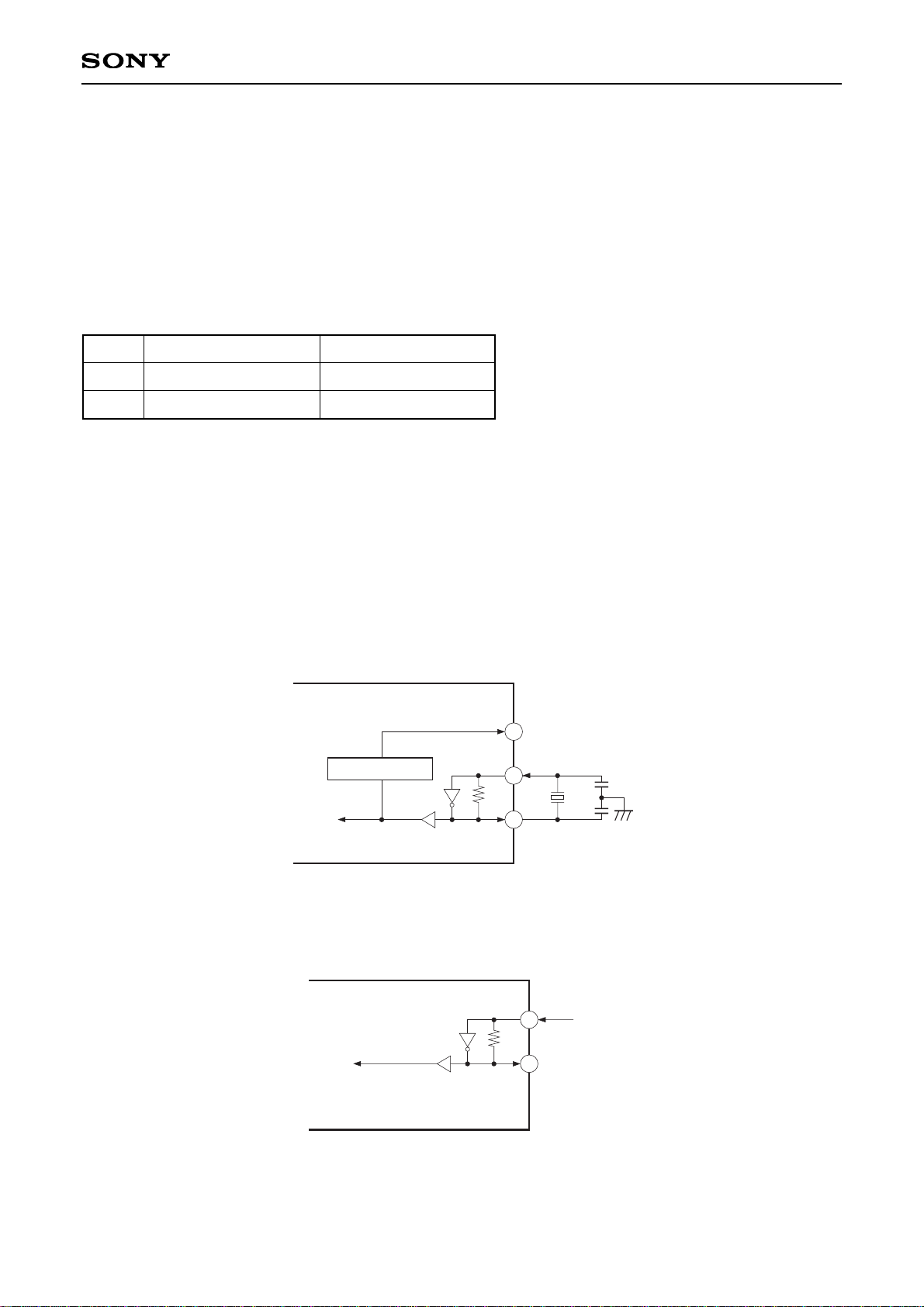
The measurement circuit in Figure 1-1 is used. Unless otherwise indicated, the measurement conditions are as
given below.
• Input signal ...1.0Vrms, 1kHz
• fs....................44.1kHz
• Rin.................0Ω
Item
S/N ratio
THD + N
Dynamic range
Channel separation
Level difference between
channels
Analog full-scale input level
∗1
ADC input impedance
Analog current consumption
1.0Vrms, EIAJ (with “A” weighting filter)
1.0Vrms, EIAJ
0.5Vrms, EIAJ
EIAJ
Only ADC characteristics using DAC1,
EIAJ
Only ADC characteristics using DAC1
Rin = 0Ω
Rin = 22kΩ
80 88
0.016
0.012
92
108
0.05
1.26
2.06
34.6
21
0.03
Measurement conditions Min. Typ. Max.
∗1
Analog input level which outputs digital full scale.
An optional analog input signal level Vin (Vrms) of 1.26Vrms or more can be set in digital full scale by the
measurement circuit external resistor Rin.
The calculation formula for external resistor Rin is:
Rin = 27.5 × Vin – 34.6 [kΩ]......(1)
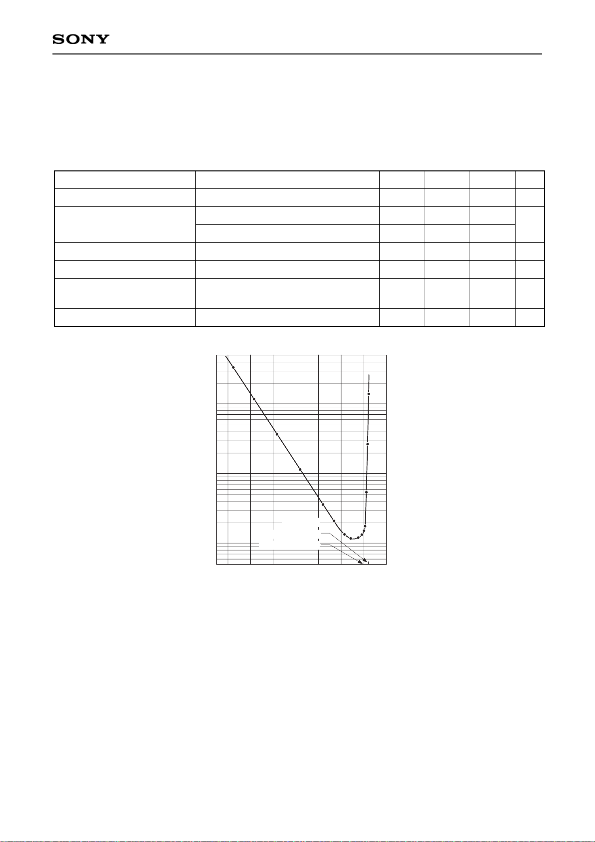
However, THD + N characteristics deteriorate for full-scale output as shown in Graph 1, so use of up to 80%
(when Rin = 0Ω, 0.8 × 1.26 (Vrms) = 1.0 (Vrms) →“analog full scale”) of the analog signal level is recommended
for digital full-scale output.
In this case, the Rin calculation formula is the same as formula (1), except that Vin becomes 1.25 × Vin.
Note that this change causes the output level after ADC + DAC to change.
Most of the above specifications are measurement values for analog full scale.
Unit
dB
%
dB
dB
dB
Vrms
kΩ
mA
– 10 –
CXD2720Q-2
[2] DAC unit characteristics
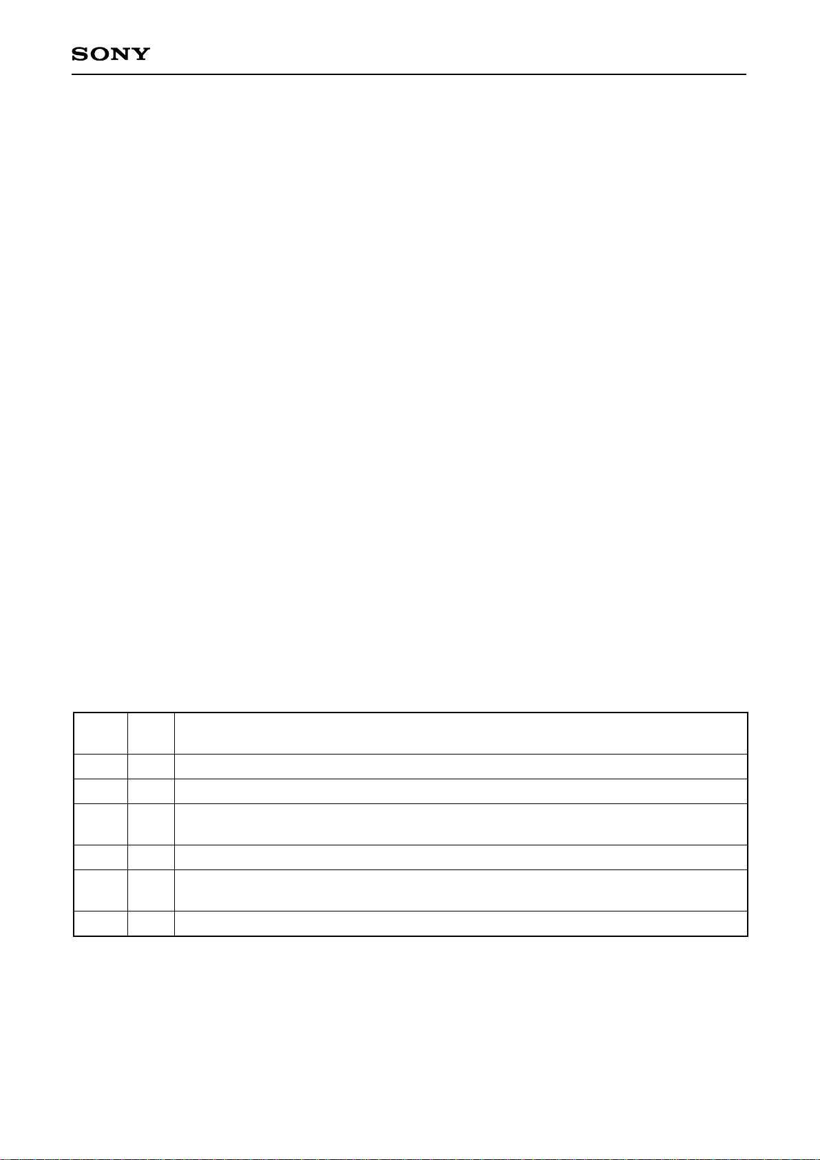
Use the measurement circuit in Figure 1-2. Unless otherwise specified, the measurement conditions are as
follows.
• Input signal....0dB, 1kHz, 16 bits
• fs....................44.1kHz
Item
S/N ratio
THD + N
Dynamic range
Channel separation
Level difference between
channels
Output level
EIAJ (with “A” weighting filter)
EIAJ (0dB)
EIAJ (–1dB)
EIAJ (–60dB)
EIAJ
EIAJ
EIAJ (Measure at OUT in Figure 1-2.)
98
0.006
0.004
98
120
0.05
2.0
dB
%
dB
dB
dB
Vrms
Measurement conditions Min. Typ. Max. Unit
Analog input level [dBV]
–60
–50 –40 –30 –20 –10 0 10
(1Vrms)
0.01
0.10
1.00
THD + N [%]
Digital full scale
Analog full scale
(Rin = 0Ω)
Graph 1.

– 11 –
CXD2720Q-2
OUT
8200p
2.2k2.2k
820p
39k
150p
22k12k
22k12k
330p
150p
39k
1M
Rin
10µ
Vin
AINx AOxN
AOxP
CXD2720Q-2
(Master mode)
Figure 1-1. ADC + DAC Measurement Circuit Diagram
OUT
8200p
2.2k2.2k
820p
39k
150p
22k12k
22k12k
330p
150p
39k
LRCK AOxN
AOxP
CXD2720Q-2
(Slave mode)
SI
XTLI
BCK
768fs
48fs
fs
DATA
(fs = 44.1kHz)
Figure 1-2. DAC Measurement Circuit Diagram
– 12 –
CXD2720Q-2
Description of Functions
1. Master/Slave Modes
[Relevant pins] XMST, LRCK, BCK
When connecting multiple CXD2720Q-2s, or when using as a pair with a D/A converter such as the
CXD2558M, one of the CXD2720Q-2 should be in master mode to supply LRCK and BCK.
The clock applied to LRCK and BCK in slave mode must be synchronized to either the crystal oscillator clock
of the XTLI and XTLO pins or the external clock input from the XTLI pin
XMST
H
L
Slave mode
Master mode
Input
Output
Mode LRCK, BCK I/O
2. Master Clock System
[Relevant pins] XTLI, XTLO, BFOT
768fs (fs = 44.1kHz) is assumed for the master clock system, and the connection is as shown below. (Please
inquire with regard to use at other than fs = 44.1kHz.)
(1) Master
Table 1-1. LRCK, BCK Mode Setting
768fs
XTLO
Frequency divider
XTLI
BFOT
768fs
384fs
O
I
O
768fs
XTLO
XTLI
O
I
768fs
OPEN
(2) Slave
– 13 –
CXD2720Q-2
3. Input/Output Synchronization Circuit
[Relevant pins] LRCK, XWO
During normal operation, synchronization is performed automatically to input LRCK (in slave mode), and phase
is matched with serial input data, but if there is a lot of jitter on LRCK, or during power input, synchronization
may be impossible. In this case, forced synchronization can be done by making the XWO pin Low for 2/Fs or
more. Forced synchronization operation is done by the timing of the second LRCK rising edge after the XWO
pin is made Low. When synchronization is completed, return the XWO pin to High.
4. Reset Circuit
[Relevant pins] XRST, XTLI, XTLO
This LSI must be reset after power is turned ON.
Reset is done by making the XRST pin Low for 1/Fs or more after supply voltage satisfies the recommended
operating condition, and the crystal oscillator clock of the XTLI, XTLO pins or the external clock input from the
XTLI pin is correctly applied.
5. Serial Audio Interface (SIF)
[Relevant pins] SI, SO, BCK, LRCK, XS24, XMST
Serial data is used for the external communication of the digital audio data.
The CXD2720Q-2 has one system each for input and output, and each one inputs/outputs 2 channels of data
at 1 sampling cycles. Either the 32-bit clock mode or 24-bit clock mode can be selected. In master mode, the
32-bit clock mode is fixed.
(1) Pin Configuration
The pins shown in the table below are assigned to SIF.
Pin
name
SI
SO
BCK
LRCK
XS24
XMST
I
O
I/O
I/O
I
I
Serial input; taken synchronized to BCK.
Serial output; output synchronized to BCK.
BCK input/output; either 32-bit clock mode (64fs) or 24-bit clock mode (48fs). BCK output
supports 32-bit clock mode only.
LRCK input/output (1fs).
SI0 slot number (24/32) selection input. Low: 24-bit slot; High: 32-bit slot. Valid only in slave
mode. Set High in master mode.
BCK, LRCK master mode/slave mode switching input. Low: master mode; High: slave mode.
I/O
Function
Table 5-1. Pin Configuration
– 14 –
CXD2720Q-2
(2) Operation Modes
The LRCK/BCK mode and SI/SO system settings can be selected by the setup register settings as follows.
LRCK/BCK Mode Setting
Setup register
SQ11
SQ10
SQ09
LRCK format
LRCK polarity selection
BCK polarity selection relative to LRCK edge
“0” : normal, “1” : IIS
“0” : Lch High, “1” : Lch Low
“0” : edge↓, “1” : edge↑
Function Contents
Table 5-2. LRCK/BCK Mode Setting
SI/O System Register Setting
SI system
Setup register
SQ08
SQ07
SQ06
SQ05
SI data list
SI frontward/rearward truncation
SI data word length
SI data word length
“0” : MSB first, “1” : LSB first
“0” : Forward truncation,
“1” : Rearward truncation
SQ06 SQ05
0 0 : 16 bits
1 1 : 24 bits
Function Contents
Table 5-3. SI System Register Setting
SO system
Setup register
SQ04
SQ03
SQ02
SQ01
SO data list
SO forward/rearward truncation
SO data word length
“0” : MSB first, “1” : LSB first
“0” : Forward truncation,
“1” : Rearward truncation
SQ02 SQ01
0 0 : 16 bits
0 1 : 18 bits
1 0 : 20 bits
1 1 : 24 bits
Function Contents
Table 5-4. SO System Register Setting
– 15 –
CXD2720Q-2
(3) SIF Format
Serial I/F have one input/output system each, and except for slot number, the following formats can be set
independently for input and output, by setting the setup register. It can also be made to support IIS format, to
enable connection to Philips and other devices. The timing charts for each data format are given on the
following pages.
32-bit slot (XS24 = High)
MSB first 24 bits Forward truncation
MSB first 16 bits Rearward truncation
LSB first 24 bits Rearward truncation
1
0
1
SQ05 SQ06 SQ07
1
0
1
0
1
1
SQ08
0
0
1
Supplement
Supports 20, 16 bits
Supports 20, 16 bits
SI format
Setup register
Table 5-5. 32-bit Slot Serial IN
MSB first 16 bits Rearward truncation
MSB first 18 bits Rearward truncation
MSB first 20 bits Rearward truncation
MSB first 24 bits Rearward truncation
MSB first 24 bits Forward truncation
LSB first 24 bits Rearward truncation
0
1
0
1
1
1
SQ01 SQ02 SQ03
0
0
1
1
1
1
1
1
1
1
0
1
SQ04
0
0
0
0
0
1
SO format
Setup register
Table 5-6. 32-bit Slot Serial OUT
24-bit slot (XS24 = Low)
MSB first 16 bits Rearward truncation
MSB first 24 bits
LSB first 24 bits
0
1
1
SQ05 SQ06 SQ07
0
1
1
1
∗
∗
SQ08
0
0
1
Supplement
Supports 20, 16 bits for forward
truncation
Supports 20, 16 bits for rearward
truncation
SI format
Setup register
Table 5-7. 24-bit Slot Serial IN
MSB first 16 bits Rearward truncation
MSB first 18 bits Rearward truncation
MSB first 20 bits Rearward truncation
MSB first 24 bits
LSB first 24 bits
0
1
0
1
1
SQ01 SQ02 SQ03
0
0
1
1
1
1
1
1
∗
∗
SQ04
0
0
0
0
1
SO format
Setup register
Table 5-8. 24-bit Slot Serial OUT
Note 1) When performing 20-bit and 16-bit data input in serial IN 24-bit data format, fill the lower 4 and 8 bits
with “0”, respectively.
Note 2) ∗ means “don't care”.
 Loading...