

Sony CXD2719Q Datasheet
Single-Chip Dolby Pro Logic Surround Decoder
Description
The CXD2719Q is a CMOS LSI developed for
Dolby Pro Logic Surround. A SRAM for short delay
and AD/DA converters are built in, and all functions
necessary for Dolby Pro Logic Surround such as an
adaptive matrix, a passive decoder including BNR,
auto input balance, a noise sequencer and center
channel mode control are contained on a single
chip.
Features
• Dolby Pro Logic Surround decoding with a single
chip
• 2-channel 1-bit AD converter, decimation filter and
prefilter operational amplifier
• 4-channel 1-bit DA converter, oversampling filter
and post filter
• Analog switch for DSP bypass
• Analog electronic attenuator (+1.5 to –29.5dB) for
center/surround channel trim
• 24K-bit SRAM for short delay
• No separation or other variance for digital
processing
• External parts reduced by incorporating analog
circuits
Functions
• Adaptive matrix
• Center channel mode control
(Normal/Phantom/Wide)
• Dolby 3 Stereo
• Auto input balance control (ON/OFF)
• Noise sequencer
• Variable delay time (0 to 34.8ms)
• 7 kHz low-pass filter (12dB/Oct)
• Modified Dolby B-type NR
• Simple SFC function
• SFC mode
• DSP bypass mode (L, R-channel through)
Structure
Silicon gate CMOS
Applications
Equipment having Dolby Pro Logic Surround
function such as AV amplifiers, receivers and
compact music systems
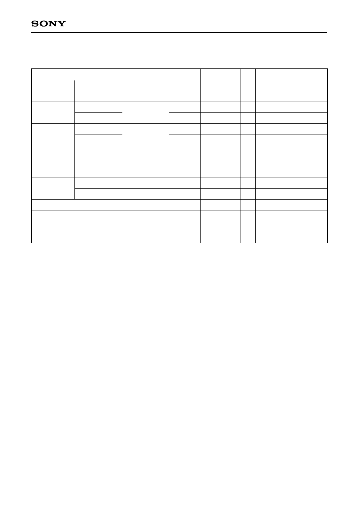
Absolute Maximum Ratings (Ta = 25°C, VSS = 0V)
• Supply voltage VDD VSS – 0.5 to +7.0 V
• Input voltage VI VSS – 0.5 to VDD + 0.5 V
• Output voltage VO VSS – 0.5 to VDD + 0.5 V
• Operating temperature
Topr –20 to +70 °C
• Storage temperature
Tstg –55 to +150 °C
Recommended Operating Conditions
• Supply voltage VDD
Analog system 4.75 to 5.25 (5.0 typ.) V
Digital system 4.50 to 5.25 (5.0 typ.) V
• Operating temperature
Ta –20 to +70 °C
Input/Output Capacitance
• Input capacitance CIN 9 (max.) pF
• Output capacitance COUT 11 (max.) pF
• Input/output capacitance
CI/O 11 (max.) pF
∗
Measurement conditions: VDD = VI = 0V, F = 1MHz
Maximum Current Consumption
(Ta = 25°C, VDD = 5.25V)
• Digital/analog block total: 166.7mA
Dolby level
• During analog input: 200 to 300mVrms
• During digital input: –20dBFS
Analog characteristics
Pro Logic ON: Dolby level = 300mVrms
Prefilter gain = –3.52dB
• S/N: L, Rch = 80dB, C, Sch = 72dB
• THD + N: L, Rch = 0.015%, C, Sch = 0.03%
∗
All values for typ.
– 1 –
E98944-PS
Sony reserves the right to change products and specifications without prior notice. This information does not convey any license by
any implication or otherwise under any patents or other right. Application circuits shown, if any, are typical examples illustrating the
operation of the devices. Sony cannot assume responsibility for any problems arising out of the use of these circuits.
CXD2719Q
80 pin QFP (Plastic)
This device is available only to parties obtaining the license from Dolby Laboratories Licensing Corporation.
"Dolby", the double-D symbol and "Pro Logic" are trademarks of Dolby Laboratories Licensing Corporation.
– 2 –
CXD2719Q
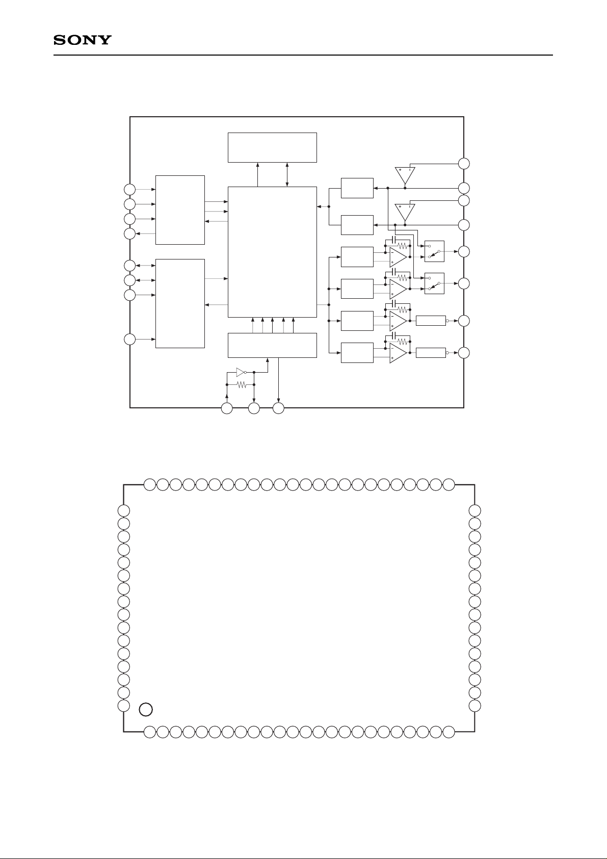
Block Diagram
XSOUT
XCOUT
ROUT
LOUT
LO2
RIN
LO1
LIN
17
23
30
35
32
42
57
58
DAC1
DAC2
DAC3
DAC4
Trim Vol
Trim Vol
ADC2
ADC1
Analog SW
Analog SW
DSP
24K bit DELAY RAM
CLOCK GENERATOR
/TIMING CIRCUIT
MICROCOMPUTER
I/F
SERIAL
DATA
I/F
26
27
39
38
55
60
46
47
49
50
33
XTLI
XTLO
BFOT
XMST
SI
BCK
REDY
XLAT
SCK
RVDT
LRCK
(Phase Inverted Output)
(Phase Inverted Output)
Pin Configuration
T.P
T.P
T.P
T.P
V
SS
0
T.P
T.P
T.P
TST0
V
DD
0
V
SS
1
TST1
TST2
TST3
TST4
XRST
BFOT
CSL1
CSL2
V
SS
2
AVS3
AVD3
LOUT
AVD1
V
SS
6
T.P
T.P
T.P
BCK
T.P
SI
T.P
V
SS
4
V
DD
1
XS24
RVDT
T.P
REDY
SCK
V
SS
3
AVS4
AVD4
ROUT
AVD2
AVS1
LO1
LIN
AVD5
AVS5
XCOUT
AVDX
XTLO
XTLI
AVSX
XSOUT
AVS6
AVD6
RIN
LO2
AVS2
XLAT
V
SS
5
LRCK
XMST
1
4
5
6
7
8
9
10
2
3
11
12
13
14
15
16
17
18
19
20
21
22
23
24
25
26
27
28
29
30
31
32
33
34
35
36
37
38
39
40
41
42
43
44
45
46
47
48
49
50
51
52
53
54
55
56
57
58
59
60
61
6364
62
65
66
67
68
69
70
71
72
73
74
75
76
77
78
79
80
T.P
T.P
T.P
T.P
T.P
T.P
V
SS7
V
DD2
T.P
T.P
T.P
T.P
T.P
T.P
T.P
T.P
– 3 –
CXD2719Q
Pin Description Notations in parentheses indicate the fixed pin connection status.
1 to 3
4
5 to 8
9
10
11
12
13
14
15
16
17
18
19
20
21
22
23
24
25
26
27
28
29
30
31
32
33
34
35
36
37
T.P
VSS0
T.P
TST0
VDD0
VSS1
TST1
TST2
TST3
TST4
XRST
BFOT
CSL1
CSL2
VSS2
AVS3
AVD3
LOUT
AVD1
AVS1
LO1
LIN
AVD5
AVS5
XCOUT
AVDX
XTLO
XTLI
AVSX
XSOUT
AVS6
AVD6
O
—
O
I
—
—
I
I
I
I
I
O
I
I
—
—
—
O
—
—
O
I
—
—
O
—
O
I
—
O
—
—
Test monitor. Normally outputs Low. (OPEN)
Digital GND. (VSS)
Test monitor. Normally outputs Low. (OPEN)
Test. Normally fixed Low. (VSS)
Digital power supply. (VDD)
Digital GND. (VSS)
Test. Normally fixed Low. (VSS)
Test. Normally fixed Low. (VSS)
Test. Normally fixed Low. (VSS)
Test. Normally fixed Low. (VSS)
System reset input. Reset when Low.
Clock, frequency-division output. [384/768/256/512fs]
Test. Normally fixed High. (VDD)
Test. Normally fixed Low. (VSS)
Digital GND. (VSS)
L-ch DA converter GND. (AVSS)
L-ch DA converter power supply. (AVDD)
L-ch DA converter output.
L-ch AD converter power supply. (AVDD)
L-ch AD converter GND. (AVSS)
L-ch AD converter LPF operational amplifier inverted output.
L-ch AD converter analog input.
C-ch DA converter power supply. (AVDD)
C-ch DA converter GND. (AVSS)
C-ch DA converter output.
Analog power supply for master clock. (AVDD)
Crystal oscillator circuit output.
Crystal oscillator circuit input.
Analog GND for master clock. (AVSS)
S-ch DA converter output.
S-ch DA converter GND. (AVSS)
S-ch DA converter power supply. (AVDD)
Pin No. Symbol I/O Description
(OPEN): Open, (VDD): +5V digital power supply, (AVDD): +5V analog power supply,
(VSS): Digital GND, (AVSS): Analog GND
– 4 –
CXD2719Q
Notations in parentheses indicate the fixed pin connection status.
(OPEN): Open, (VDD): +5V digital power supply, (AVDD): +5V analog power supply,
(VSS): Digital GND, (AVSS): Analog GND
∗
There are three digital and seven analog power supplies, but the power-on sequence is not specified.
Pin No.
38
39
40
41
42
43
44
45
46
47
48
49
50
51
52
53
54
55
56
57
58
59
60
61 to 63
64
65 to 72
73
74
75 to 80
Symbol
RIN
LO2
AVS2
AVD2
ROUT
AVD4
AVS4
VSS3
SCK
REDY
T.P
XLAT
RVDT
XS24
VDD1
VSS4
T.P
SI
T.P
BCK
LRCK
VSS5
XMST
T.P
VSS6
T.P
VDD2
VSS7
T.P
I/O
I
O
—
—
O
—
—
—
I
O
O
I
I
I
—
—
O
I
I
I/O
I/O
—
I
O
—
O
—
—
O
Description
R-ch AD converter analog input.
R-ch AD converter LPF operational amplifier inverted output.
R-ch AD converter GND. (AVSS)
R-ch AD converter power supply. (AVDD)
R-ch DA converter output.
R-ch DA converter power supply. (AVDD)
R-ch DA converter GND. (AVSS)
Digital GND. (VSS)
Shift clock input for microcomputer interface.
Transfer enabling signal output for microcomputer interface. Transfer prohibited when Low.
Test monitor. Normally outputs Hi-Z. (OPEN)
Latch input for microcomputer interface.
Data input for microcomputer interface.
Serial data 24-/32-bit slot selection. 24-bit slot when Low. (valid for slave mode)
Digital power supply. (VDD)
Digital GND. (VSS)
Test monitor. Normally outputs Low. (OPEN)
1-sampling 2-channel serial data input.
Test input. Normally inputs Low. (VSS)
Serial bit transfer clock for serial I/O data SI and SO.
Sampling frequency clock for serial I/O data SI and SO.
Digital GND. (VSS)
BCK, LRCK master/slave mode switching input. Master mode when Low.
Test monitor. Normally outputs Low. (OPEN)
Digital GND. (VSS)
Test monitor. Normally outputs Low. (OPEN)
Digital power supply. (VDD)
Digital GND. (VSS)
Test monitor. Normally outputs Low. (OPEN)
– 5 –
CXD2719Q
DC Characteristics
(AVD1 to 6 = AVDX = VDD0 to 2 = 5V ± 5%, AVS1 to 6 = AVSX = VSS0 to 7 = 0V, Ta = –20 to +70°C)
Item
Symbol
Conditions Min. Max. Unit Applicable pinsTyp.
V
V
V
V
V
V
V
V
V
V
V
µA
µA
µA
Ω
∗1, ∗2, ∗7
∗1, ∗2, ∗7
∗5
∗5
∗3, ∗6
∗3, ∗6
∗4
∗8, ∗9
∗8, ∗9, ∗10
∗11
∗11
∗1, ∗5, ∗7
∗2, ∗3, ∗6
∗9, ∗10
Resistance between ∗7and
∗11
High level
Low level
High level
Low level
High level
Low level
High level
Low level
High level
Low level
Input voltage
(1)
Input voltage
(2)
Input voltage
(3)
Input voltage (4)
Output voltage
(1)
Output voltage
(2)
Input leak current (1)
Input leak current (2)
Output leak current
Feedback resistance
VIH
VIL
VIH
VIL
VIH
VIL
VIN
VOH
VOL
VOH
VOL
II
II
IOZ
RFB
CMOS input
Schmitt input
TTL input
Analog input
IOH = –2.0mA
IOL = 4.0mA
IOH = –12.0mA
IOL = 12.0mA
VIH = VDD, VSS
VIH = VDD, VSS
VIH = VDD, VSS
0.7VDD
0.8VDD
2.2
VSS
VDD – 0.8
VDD/2
–10
–40
–40
250k 1M
0.3VDD
0.2VDD
0.8
VDD
0.4
VDD/2
10
40
40
2.5M
∗1
CSL2, CSL1, TST0 to TST4, XMST
∗2
XLAT, RVDT, XS24, SCK
∗3
SI
∗4
LIN, RIN
∗5
XRST
∗6
During input to bidirectional pins BCK, LRCK
∗7
XTLI
∗8
During output from bidirectional pins BCK, LRCK
∗9
BFOT
∗10
REDY
∗11
XTLO
– 6 –
CXD2719Q
AC Characteristics
(AVD1 to 6 = AVDX = VDD0 to 2 = 5V ± 5%, AVS1 to 6 = AVDX = VSS0 to 7 = 0V, Ta = –20 to +70°C)
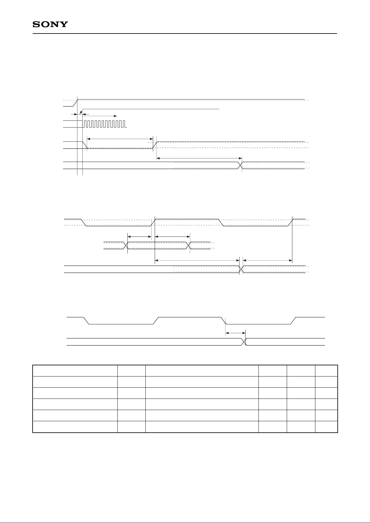
Input Timing from Power-on to Input Pin
•••••
VDD
XTLI
XRST
Input pins
0.7V
DD
0.3VDD
1/fs or more
1/fs or more
Determined by the crystal and other external circuit conditions
Stable (clock applied correctly)
0.8V
DD
0.2VDD
0.95VDD
First input
BCK
SI
LRCK
tHLR tSLR
0.7V
DD
0.3VDD
0.7VDD
0.3VDD
tSSI tHSI
0.7V
DD
0.3VDD
BCK
LRCK
tDLR
Serial Audio Interface Timing
[Slave mode]
[Master mode]
Item
SI setup time
SI hold time
LRCK setup time
LRCK hold time
LRCK delay time
Symbol
tSSI
tHSI
tSLR
tHLR
tDLR
Conditions
Slave mode
Slave mode
Slave mode
Slave mode
Master mode, CL = 120pF
Min.
20
40
20
40
Max.
50
Unit
ns
ns
ns
ns
ns
– 7 –
CXD2719Q
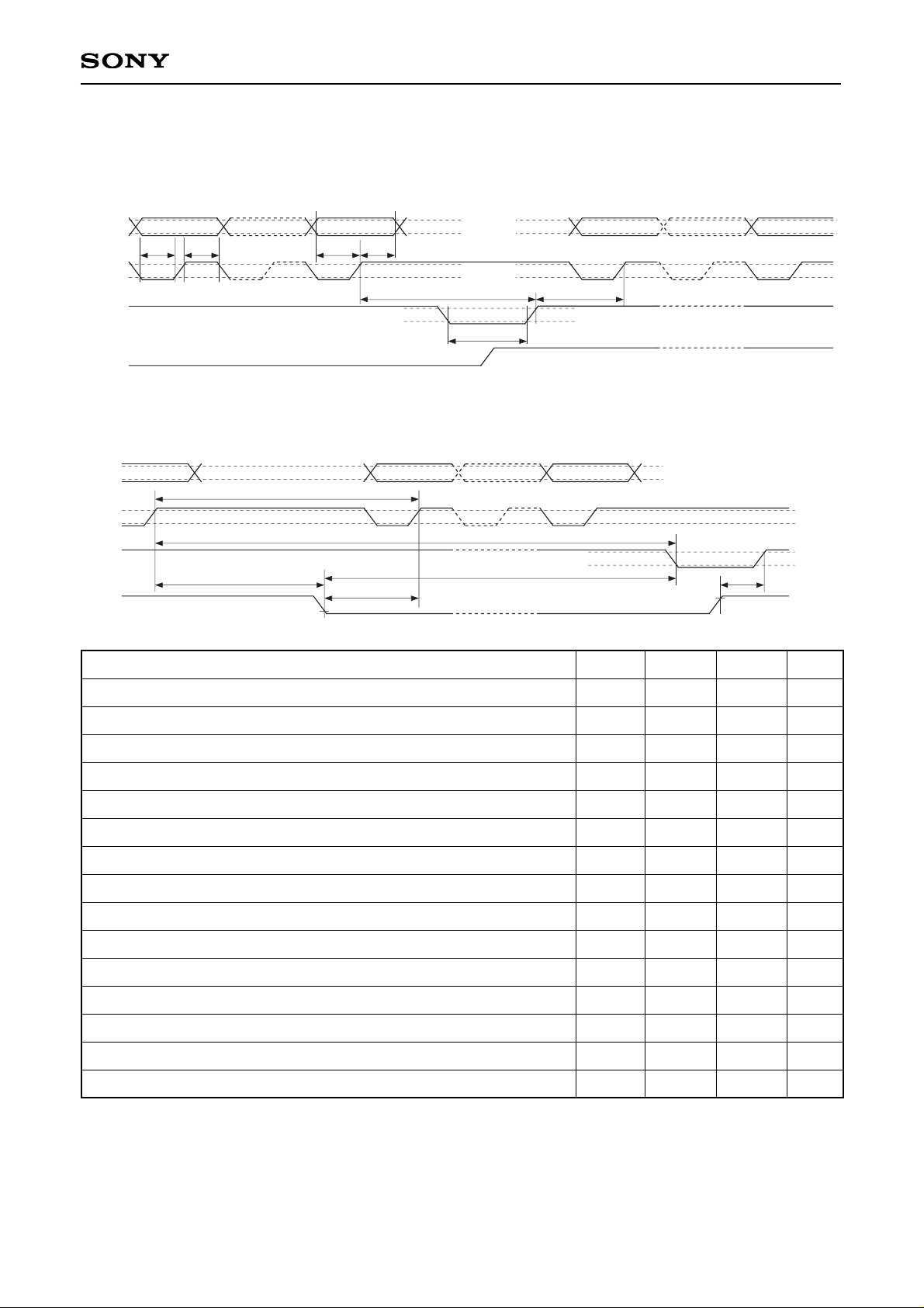
Microcomputer Interface Timing
Transfer timing for address section, transfer mode section and data section LSB
Transfer timing from data section MSB to address section and transfer mode section
Notes) 1. t is the cycle of 2/3 the clock frequency applied to the XTLI pin. (512fs)
2. The REDY pin is the value for CL = 60pF.
Item
RVDT data setup time relative to SCK rise
RVDT data hold time from SCK rise
SCK Low level width
SCK High level width
XLAT Low level width
XLAT High level width
SCK rise preceding time relative to XLAT rise
SCK rise wait time relative to XLAT rise
Delay time to REDY fall relative to SCK rise
REDY fall preceding time relative to SCK rise
REDY rise preceding time relative to XLAT rise
REDY rise preceding time relative to SCK fall
XLAT fall wait time relative to SCK rise
XLAT fall delay time relative to REDY fall
SCK rise wait time for next transfer
Symbol
tDS
tDH
tSWL
tSWH
tLWL
tLWH
tSLP
tLSD
tSBD
tBSP
tRLP
tRSDP
tSLD
tLDR
tSS
Min.
20
1t + 20
1t + 20
1t + 20
1t + 20
1t + 20
20
3t + 20
20
20
20
3t + 20
20
2t + 40
Max.
4t + 50
Unit
ns
ns
ns
ns
ns
ns
ns
ns
ns
ns
ns
ns
ns
ns
ns
RVDT
SCK
tSWL
tSWH tDS tDH
Address LSB Mode MSB
0.3VDD
0.7VDD
0.3VDD
0.7VDD
tSLP tLSD
tLWL
0.3VDD
0.7VDD
XLAT
REDY
Data LSB Data MSB
RVDT
SCK
XLAT
REDY
Mode MSB
0.3V
DD
0.7VDD
Address LSBData MSB
tSS
tLDR
tSBD
tSLD
tBSP
0.3V
DD
0.7VDD
tRLP
0.3V
DD
0.7VDD

– 8 –
CXD2719Q
Analog Characteristics
(AVD0 to 6 = VDD0 to 2 = AVDX = 5.0V, AVS0 to 6 = VSS0 to 7 = AVSX = 0.0V, fs = 44.1kHz, Ta = 25°C)
When Pro Logic mode is on, the input signal level while measuring the center (C) and surround (S) channels
should be –3dB smaller than the input level while measuring the left (L) and right (R) channels. Note that the C
channel is input in-phase to the L channel, and the S channel is input at reversed phase to the R channel.
The input level is the same for all measurement items when Pro Logic mode is off.
1. ADC + DAC Connection Total Characteristics
I
n addition to the ADC and DAC, the total characteristics include the prefilter with built-in operational amplifier,
built-in post filter, and trim volume. Use the analog I/O circuits in the Application Circuit for the measurement
circuit.
1-1. When Pro Logic mode is on
Unless otherwise specified, the measurement conditions are as given below.
• VIN (L, R) = 300mVrms, VIN (C, S) = 212mVrms (= 0dB)
• fIN = 1kHz
∗1
When VIN = 200mVrms (= –3.52dB), the S/N ratio is 3.52dB smaller than the values noted in the table above.
∗2
VIN (L, R) = 2.0Vrms, VIN (C, S) = 1.414Vrms
∗3
VIN (L, R) = 300mVrms, VIN (C, S) = 212mVrms
∗4
VIN (L, R) = 200mVrms, VIN (C, S) = 141mVrms
∗5
When the L and R channel gain deviation is 0.1dB or less for the ADC front-end prefilter output.
∗6
Includes the amplification (L/Rch...5.27dB
, C/Sch...13.72dB) of the external amplifier.
∗7
The trim volume is set to 0dB.
L, R
C, S
L, R
C
S
L, R
C, S
L, R
C, S
L, R
C, S
L, R
C
S
L, R
C, S
(all)
(all)
L, R
C, S
∗7
70
65
25
25
250
80
72
60
56
64
0.04
0.007
0.015
0.03
0.02
0.04
0.12
0.18
0.04
16.5
60
40
280
±0.2
36
91
3.9
–13.2
1.00
1.00
310
dB
%
dB
dB
Vrms
dB
mA
dB
S/N ratio
∗1
THD + N
Head room
Matrix rejection
Output level
Level difference between channels
Current consumption
Power supply rejection
ratio
∗6
CCIR/ARM filter
10Hz to 500kHz
10Hz to 20kHz
VIN = 16.5dB
∗2
10Hz to 20kHz
VIN = 0dB
∗3
10Hz to 20kHz
VIN = –3.52dB
∗4
10Hz to 500kHz
10Hz to 20kHz, THD + N = 1%
∗5
Analog system (including oscillator circuit)
Digital system
1mVrms
, 100Hz sine wave
Channels Min. Typ. Max. UnitItem Measurement conditions
– 9 –
CXD2719Q
1-2. When Pro Logic mode is off
Unless otherwise specified, the measurement conditions are as given below.
• VIN (L, R, C, S) = 2.0Vrms (= 0dB)
• fIN = 1kHz
L, R
C, S
(all)
L, R
C, S
L, R
C, S
(all)
(all) 1.7
97
90
0.03
0.004
0.01
93
83
1.33
1.85
1.00
2.0
dB
%
dB
Vrms
Vrms
S/N ratio
THD + N
∗11
Dynamic range
∗12
ADC maximum input level
∗13
Output level
∗14
EIAJ
(with "A" weighting filter)
EIAJ (0dB)
EIAJ (–3dB)
EIAJ (–60dB)
(Full-scale output)
∗11
See Graphs 1a and 1b.
∗12
THD + N during –60 dB input
∗13
The analog input level at which the ADC outputs full scale varies according to supply voltage AVDn.
When supply voltage AVDn contains deviation, calculate the maximum input level from (Formula 1) below
and adjust the level with the ADC front-end prefilter, etc., so that the waveform is not clipped at the
minimum voltage.
ADC maximum input level [Vrms] = 1.33 [Vrms] × (Formula 1)
∗14
Like the ADC, the DAC conversion gain also varies according to supply voltage AVDn. However, the DAC
has the reverse characteristics of the ADC, so the total gain between the ADC and DAC is constant.
Minimum supply voltage [V]
5.0 [V]
–60 –50 –40 –30 –20 –10 0
0.001
0.01
0.1
1
10
Graph 1a. L, R Channel Characteristics
Analog input level [dB]
THD + N [%]
0dB = 2Vrms
fin = 1kHz
–60 –50 –40 –30 –20 –10 0
0.001
0.01
0.1
1
10
Graph 1b. C, S Channel Characteristics
Analog input level [dB]
THD + N [%]
0dB = 2Vrms
fin = 1kHz
Channels Min. Typ. Max. UnitItem Measurement conditions
– 10 –
CXD2719Q
2. DAC Characteristics
In addition to the DAC, these characteristics include the built-in post filter and trim volume. Use the digital input
and analog output circuits in the Application Circuit for the measurement circuit.
2-1. When Pro Logic mode is on
Unless otherwise specified, the measurement conditions are as given below.
• Digital data = –20dBFS
• fIN = 3kHz
Channels
L, R
C, S
L, R
C
S
L, R
C
S
L, R
C
S
L, R-in
C-in
S-in
(all)
Min. Typ.
77
68
60
52
65
0.05
0.08
0.06
0.15
0.3
0.08
–20
200
62
87
79
±0.2
Max. Unit
dB
%
dBFS
mVrms
dB
dB
Item
S/N ratio
THD + N
Dolby level
Output level
∗31
Matrix rejection
Level difference between
channels
Measurement conditions
CCIR/ARM filter
Data = –20dBFS
10Hz to 500kHz
Data = –20dBFS
10Hz to 20kHz
Data = –20dBFS
10Hz to 500kHz
Data = –20dBFS
Data = –20dBFS
fIN = 3kHz
∗31
The output level depends on supply voltage AVDn as shown in (Formula 2) below.
Output level [mVrms] = 285 [mVrms] × (Formula 2)
Supply voltage AVDn [V]
5.0 [V]

– 11 –
CXD2719Q
2-2. When Pro Logic mode is off
Unless otherwise specified, the measurement conditions are as given below.
• Digital data = Full scale (0dBFS)
• fIN = 1kHz
Channels
L, R
C, S
L, R
C, S
L, R
C, S
L, R
C, S
(all)
Min. Typ.
100
91
0.03
0.007
0.007
0.01
87
83
2.0
Max. Unit
dB
%
dB
Vrms
Item
S/N ratio
THD + N
∗41
Dynamic range
∗42
Output level
∗43
Measurement conditions
EIAJ
(with "A" weighting filter)
EIAJ (0dB)
EIAJ (–3dB)
EIAJ (–60dB)
∗41
See Graphs 2a and 2b.
∗42
THD + N during –60dB input
∗43
The output level depends on supply voltage AVDn as shown in (Formula 3) below.
Output level [Vrms] = 1.9 [Vrms] × (Formula 3)
Supply voltage AVDn [V]
5.0 [V]
–60 –50 –40 –30 –20 –10 0
0.001
0.01
0.1
1
10
Graph 2b. C, S Channel Characteristics
Digital input level [dB]
THD + N [%]
0dB = Full scale
fin = 1kHz
–60 –50 –40 –30 –20 –10 0
0.001
0.01
0.1
1
10
Graph 2a. L, R Channel Characteristics
THD + N [%]
Digital input level [dB]
0dB = Full scale
fin = 1kHz
– 12 –
CXD2719Q
3. Bypass Mode Characteristics (L, R channels only)
These are the characteristics without passing through the DSP, and including the prefilter with built-in
operational amplifier and the built-in post filter. Use the analog I/O circuits in the Application Circuit for the
measurement circuit. Unless otherwise specified, the measurement conditions are as given below.
• fIN = 1kHz
• VIN (L, R) = 2.0Vrms (= 0dB)
Min. Typ.
97
100
80
0.008
0.005
95
2.5
2.0
±0.2
105
7.5
Max. Unit
dB
%
dB
Vrms
Vrms
dB
dB
dB
Item
S/N ratio
THD + N
Dynamic range
∗51
Maximum input level
Output level
Level difference between channels
Channel separation
Power supply rejection ratio
∗52
Measurement conditions
CCIR/ARM filter
10Hz to 20kHz, "A" weighting filter
10Hz to 500kHz
10Hz to 500kHz
10Hz to 20kHz
10Hz to 20kHz, VIN = –60dB
THD + N = 0.05%
1mVrms, 100Hz sine wave
Min.
10
10
Typ.
104
Max.20Unit
kΩ
dB
kΩ
kHz
Item
Prefilter
Post filter
Measurement conditions
Feedback resistance value
Maximum amplification rate
(100kHz or less)
Load resistance value
Cut-off frequency (= fc)
Min. Typ.
1.5
–29.5
1.0
Max. Unit
dB
dB
dB
Item
Maximum gain
Minimum gain
Variable step
Symbol
TRIMmax
TRIMmin
TRIMstep
∗51
THD + N during –60dB input
∗52
Includes the amplification (5.27dB) of the external amplifier.
4. Filter Characteristics
5. Trim Volume Characteristics

– 13 –
CXD2719Q
Description of Functions
1. Master/Slave Modes
[Relevant pins] XMST, LRCK, BCK
When using the CXD2719Q alone without digital input, set the CXD2719Q to master mode.
When using digital input, the CXD2719Q may be set to either master mode or slave mode.
The clock applied to LRCK and BCK in slave mode must be synchronized to either the crystal oscillator clock
of the XTLI and XTLO pins or the external clock input from the XTLI pin.
Table 1-1. LRCK, BCK Mode Setting
XMST
H
L
Mode
Slave mode
Master mode
LRCK, BCK I/O
Input
Output
SQC05
0
0
1
1
SQC04
0
1
0
1
BFOT
384fs
256fs
512fs
768fs
2. Master Clock System
[Relevant pins] XTLI, XTLO, BFOT
768fs (fs = 32 to 44.1kHz) is assumed for the master clock system, and the connection is as shown below.
BFOT outputs the clock obtained by frequency dividing the master clock. The frequency division ratio can be
changed by the setup register (SQC04, SQC05). (See "6. Setup Register".)
(1) Master
(2) Slave
O
I
O
Frequency
divider
Setup
Register
512fs
XTLI
XTLO
768fs
BFOT
256fs/384fs/512fs/768fs
O
512fs
XTLI
XTLO
768fs
I
OPEN
Frequency
divider
Fig. 2-1.
Note) Oscillation circuits may differ according to peripheral circuit and
substrate. Consult with crystal oscillator manufacturers about the
selecting oscillation circuits.
– 14 –
CXD2719Q
3. Reset Circuit
[Relevant pins] XRST, XTLI, XTLO
This LSI must be reset after the power is turned on.
Reset is done by setting the XRST pin Low for 1/fs or more after the supply voltage satisfies the recommended
operating condition, and the crystal oscillator clock of the XTLI and XTLO pins or the external clock input from
the XTLI pin is correctly applied. (See "AC Characteristics".)
4. Serial Audio Interface (SIF)
[Relevant pins] SI, BCK, LRCK, XS24, XMST
Serial data is used for the external communication of the digital audio data. The CXD2719Q has only one input
system, and 2 channels of data are input each sampling cycle. Either the 32-bit clock mode or the 24-bit clock
mode can be selected. In master mode, the mode is fixed to the 32-bit clock mode.
(1) Pin Configuration (The pins shown in the table below are assigned to the SIF.)
Serial input; taken with synchronized to BCK.
BCK I/O; either 32-bit clock mode (64fs) or 24-bit clock mode (48fs). BCK output supports
32-bit clock mode only.
LRCK I/O (1fs).
SIO slot number (24/32) selection input. Low: 24-bit slot; High: 32-bit slot.
Valid only in slave mode. Set High in master mode.
Do not switch between High and Low during DSP operation.
BCK, LRCK master mode/slave mode switching input.
Low: master mode; High: slave mode.
Symbol
SI
BCK
LRCK
XS24
XMST
I/O
Function
I
I/O
I/O
I
I
"0": normal, "1": IIS
"0": Lch "H", "1": Lch "L"
"0": edge ↓, "1" : edge ↑
Setup register
SQC15
SQC14
SQC13
Function
Contents
LRCK format
LRCK polarity selection
BCK polarity selection relative to LRCK edge
Valid only in slave mode. Fix to "0" in master
mode.
Table 4-1. Pin Configuration
Table 4-2. LRCK/BCK Mode Setting
(2) Operation Modes
The LRCK/BCK mode can be selected by the setup register settings as follows. (See "6. Setup Register".)
LRCK/BCK Mode Setting
– 15 –
CXD2719Q
Table 4-3. Setup Register Settings
(3) SIF Format
The serial audio interface has only one input system, and except for the slot number, the following formats can
be set by setting the setup register. The serial audio interface can also support IIS format to enable connection
to Philips and other company's devices.
The timing charts for each data format are given on the following page.
SQC12
0
0
1
1
SQC11
0
1
0
1
Data arrangement/Frontward or rearward truncation/Data word length
MSB first/Frontward truncation/24 bits
MSB first/Rearward truncation/16 bits
MSB first/Rearward truncation/18 bits
MSB first/Rearward truncation/20 bits
∗
All formats support either the 24- or 32-bit slot in slave mode.

– 16 –
CXD2719Q
23 22 21 20 19 18 17 16 15 14 13 12 11 10 09 08 07 06 05 04 03 02 01 00
15 14 13 12 11 10 09 08 07 06 05 04 03 02 01 00 15 14 13 12 11 10 09 08 07 06 05 04 03 02 01 00
15 14 13 12 11 10 09 08 07 06 05 04 03 02 01 0017 16 15 14 13 12 11 10 09 08 07 06 05 04 03 02 01 0017 16
15 14 13 12 11 10 09 08 07 06 05 04 03 02 01 0017 1619 18 19 15 14 13 12 11 10 09 08 07 06 05 04 03 02 01 0017 1618
LRCK
BCK
SI
23 22 21 20 19 18 17 16 15 14 13 12 11 10 09 08 07 06 05 04 03 02 01 00
• MSB first 24 bits frontward truncation (SQC12, 11 = 0, 0)
• MSB first 16 bits rearward truncation (SQC12, 11 = 0, 1)
• MSB first 18 bits rearward truncation (SQC12, 11 = 1, 0)
• MSB first 20 bits rearward truncation (SQC12, 11 = 1, 1)
Lch
Rch
LSB MSBIavalid LSB Iavalid
MSBIavalid LSB MSBIavalid LSB
LSB MSBIavalid LSB
LSB MSBIavalid LSB
MSB
MSB
Iavalid
Iavalid
MSBMSB
23 22 21 20 19 18 17 16 15 14 13 12 11 10 09 08 07 06 05 04 03 02 01 00 23 22 21 20 19 18 17 16 15 14 13 12 11 10 09 08 07 06 05 04 03 02 01 00
15 14 13 12 11 10 09 08 07 06 05 04 03 02 01 00 15 14 13 12 11 10 09 08 07 06 05 04 03 02 01 00
17 16 15 14 13 12 11 10 09 08 07 06 05 04 03 02 01 00 17 16 15 14 13 12 11 10 09 08 07 06 05 04 03 02 01 00
19 18 17 16 15 14 13 12 11 10 09 08 07 06 05 04 03 02 01 00 19 18 17 16 15 14 13 12 11 10 09 08 07 06 05 04 03 02 01 00
LRCK
BCK
SI
LSB MSB LSB
MSB LSB MSBIavalid LSB
LSB MSBIavalid LSB
LSB MSBIavalid LSB
MSB
MSB
Iavalid
Iavalid
Iavalid
Lch
Rch
MSB
• MSB first 24 bits (SQC12, 11 = 0, 0)
• MSB first 16 bits rearward truncation (SQC12, 11 = 0, 1)
• MSB first 18 bits rearward truncation (SQC12, 11 = 1, 0)
• MSB first 20 bits rearward truncation (SQC12, 11 = 1, 1)
Digital Audio Data Input Timing (with polarities: SQC15 = 0, SQC14 = 0, SQC13 = 0)
32-bit slot
24-bit slot

– 17 –
CXD2719Q
5. Microcomputer Interface
[Relevant pins] RVDT, SCK, XLAT, REDY
The CXD2719Q performs the serial audio interface format setting and the coefficient settings such as volume
and filter by serial data from the microcomputer.
(1) Pin Configuration
The four external pins indicated in the table below are assigned to the microcomputer interface.
Serial data input from microcomputer.
Shift clock for serial data. Input data from RVDT is taken according to the SCK rise.
Interprets the 8 bits of RVDT before this signal rises as transfer mode data, and the
bits before that as address data.
Transfer prohibited while at Low level. Transfer enabled at High. This pin is an open
drain, and must be pulled up externally.
Symbol
RVDT
SCK
XLAT
REDY
I/O
Function
I
I
I
O
Table 5-1. Microcomputer Interface External Pins
(2) Description of Communication Formats
The internal data transfer timing from the microcomputer interface to the coefficient RAM and setup register is
called the SV cycle, and is generated once per 1 LRCK.
The SV cycle is generated immediately preceding the signal processing program, so it has absolutely no effect
on signal processing, and there is no risk of the sound being cut.
Address section + Mode section + Data section
act as one package of data to transfer data from the microcomputer to the CXD2719Q.
[Write]∗For coefficient RAM
A0 A7 M0 M7 D0 D15
Address section (8 bits) Mode section (8 bits)
RVDT
SCK
XLAT
REDY
Data section (16 bits)
Fig. 5-1. Example of Communication
– 18 –
CXD2719Q
(3) Data Structure
The data structure is classified into three types, as shown in the table below. All data communication is done
with LSB first.
Coefficient RAM and setup register are both 16 bits
Symbol
A0 to A7
M0 to M7
D0 to D15/SQ00 to SQ15
Bit length
Remarks
8
8
16
Contents
Address section
Transfer mode section
Data section
Table 5-2. Data Structure
(3)-1. Transfer Mode Section
The transfer mode section is 8 bits and has the following functions.
Normally fixed to "0"
SU1 SU0
0 0 Field A
0 1 Field B
1 0 Field C
1 1 Field D
VS1 VS0
0 0 Setup register
1 0 Coefficient RAM
Normally fixed to "0"
Bit
M7
M6
M5
M4
M3
M2
M1
M0
Symbol
Function
SU1
SU0
VS1
VS0
Reserve
Setup Reg.
type
Data type
Reserve
Table 5-3. Transfer Mode Section
(3)-2. Address Section
The coefficient RAM has a 256-word structure, so the address section is 8 bits. The setup register has a 4word structure and the field (address) is specified by the mode section, so the address section data may be
optional.
(3)-3. Data Section
The coefficient RAM and setup register both have a 16-bit structure, so 16 SCK are required.
 Loading...