

Sony CXD2589Q Datasheet
CD Digital Signal Processor
Description
The CXD2589Q is a digital signal processor LSI for
CD players and is equipped with built-in digital
filters, zero detection circuit, 1-bit DAC, and analog
low-pass filter on a single chip.
Features
Digital Signal Processor (DSP) Block
• Playback mode supporting CAV
(Constant Angular Velocity)
– Frame jitter-free
– Allows 0.5 to double-speed continuous playback
– Allows relative rotational velocity readout
– Supports external spindle control
• Wide capture range playback mode
– Spindle rotational velocity following method
– Supports normal-speed and double-speed playback
• 16K RAM
• EFM data demodulation
• Enhanced EFM frame sync protection
• SEC strategy-based error correction
• Subcode demodulation and Sub Q data error
detection
• Digital spindle servo
• 16-bit traverse counter
• Asymmetry compensation circuit
• Serial bus-based CPU interface
• Error correction monitor signals, etc. are output
from a new CPU interface.
• Servo auto sequencer
• Digital audio interface output
• Digital peak meter
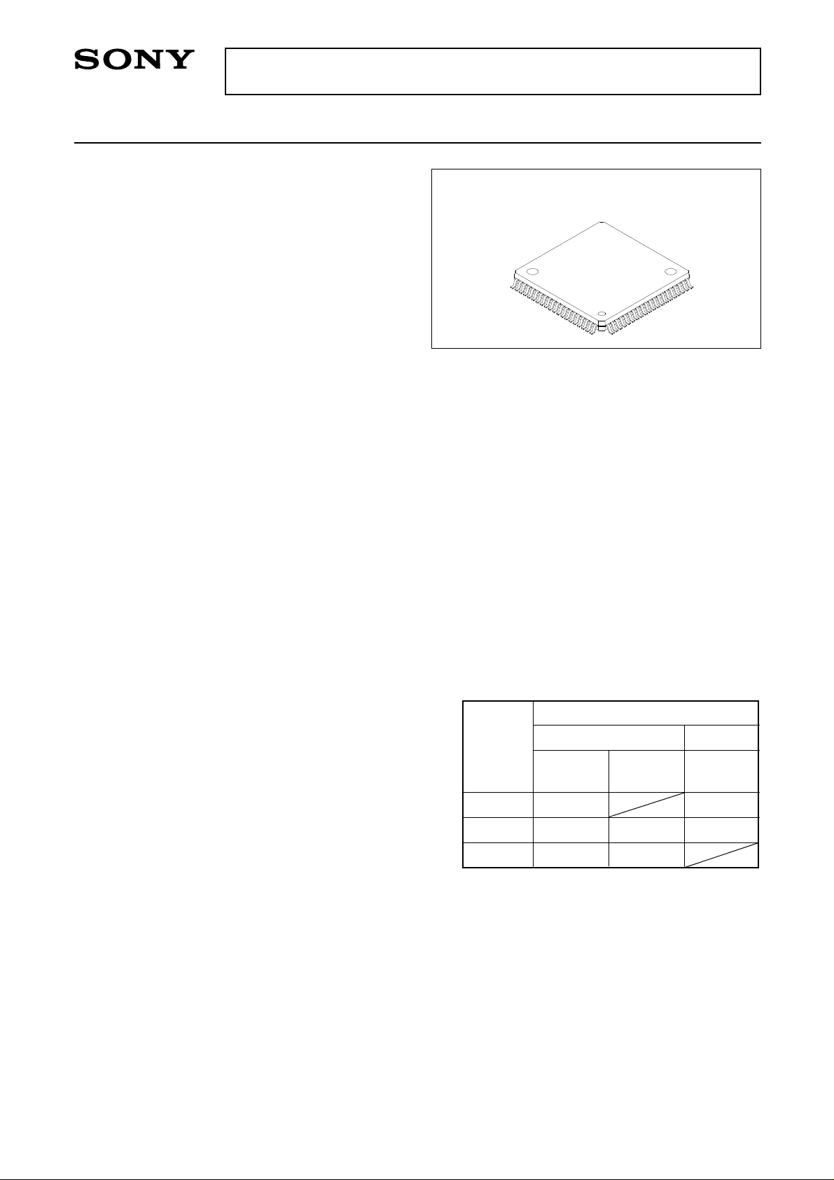
CXD2589Q
80 pin QFP (Plastic)
Absolute Maximum Ratings
• Supply voltage VDD –0.3 to +7.0 V
• Input voltage VI –0.3 to +7.0 V
(Vss – 0.3V to VDD + 0.3V)
• Output voltage VO –0.3 to +7.0 V
• Storage temperature
Tstg –40 to +125 °C
• Supply voltage difference
VSS – AVSS –0.3 to +0.3 V
VDD – AVDD –0.3 to +0.3 V
Note) AVDD includes XVDD, and AVSS includes XVSS.
Recommended Operating Conditions
• Supply voltage VDD 3.4 to 5.25 V
• Operating temperature
Topr –20 to +75 °C
Note) The VDD (min.) for the CXD2589Q varies
according to the playback speed selection.
Digital Filter, DAC, Analog Low-Pass Filter Block
• DBB (Digital Bass Boost)
• Supports double-speed playback
• Digital de-emphasis
• Digital attenuation function
• Zero detection function
• 8Fs oversampling digital filter
• S/N: 100dB or more (master clock: 384Fs typ.)
Logical value: 109dB
• THD + N: 0.007% or less
(master clock: 384Fs typ.)
• Rejection band attenuation: –60dB or less
Applications
CD players
Structure
Silicon gate CMOS IC
Sony reserves the right to change products and specifications without prior notice. This information does not convey any license by
any implication or otherwise under any patents or other right. Application circuits shown, if any, are typical examples illustrating the
operation of the devices. Sony cannot assume responsibility for any problems arising out of the use of these circuits.
– 1 –
Playback
speed
2×
1×
∗1
1×
∗1
When the internal operation of the CD-DSP
side is set to double-speed mode and the
crystal oscillation frequency is halved,
normal-speed playback results.
Input/Output Capacitances
• Input capacitance CI 12 (max.) pF
• Output capacitance CO 12 (max.) pF
Note) Measurement conditions VDD = VI = 0V
VCO high
speed
3.4
3.4 3.5
3.4 3.5
VDD (min.) [V]
CD-DSP block DAC block
VCO normal
speed
fM = 1MHz
4.5
3.4
E96Y02A73
Block Diagram
CXD2589Q
C4M
RF
ASYI
ASYO
BIAS
XPCK
FILO
FILI
PCO
CLTV
FOK
SEIN
CNIN
VPCO
XTSL
VCKI
51
26 27
25
52
35
37
38
36
48
30
31
29
33
18
10
11
Clock
Generator
Asymmetry
Corrector
Digital
PLL
Servo
Auto
Sequencer
V16M
OSC
VCTL
28
Interface
XUGF
47
demodurator
Sub Code
Processor
CPU
49
GFS
EFM
54
EMPH
56
WFCK
Error
Corrector
16K
RAM
Digital
C2PO
50
39
D/A
Interface
CLV
LRCK
41
Digital
OUT
PCMD
BCK
43
EMPHI
55
Over Sampling
BCKI
PCMDI
LRCKI
40
Serial-In
Interface
Digital Filter
PWM PWM
62
42
44
3rd-Order
Noise Shaper
SYSM
Timing
Logic
24
TES1
TEST
23
79
XRST
3
RMUT
2
LMUT
70
XTAI
71
XTAO
12
13
DATO
14
XLTO
CLKO
6
SENS
7
DATA
8
XLAT
9
CLOK
15
16
SPOA
17
SPOB
57
XLON
58
SCOR
59
SBSO
5
EXCK
4
SQSO
SQCK
21
MDP
22
PWMI
53
DOUT
74
LOUT2
75
AIN2
76
AOUT2
67
LOUT1
66
AIN1
65
AOUT1
– 2 –
Pin Configuration
60
Vss
59
SBSO
EXCK
58
SCOR
57
WFCK
56
EMPHI
55
EMPH
54
DOUT
53
52
C4M
51
XTSL
50
C2PO
49
GFS
48
XPCK
47
DD
V
XUGF
46
45
Vss
44
BCKI
43
BCK
PCMD
PCMDI
4142
CXD2589Q
VDD
SYSM
AVss
DD
AV
AOUT1
AIN1
LOUT1
AVss
DD
XV
XTAI
XTAO
XVss
AVss
LOUT2
AIN2
AOUT2
DD
AV
AVss
XRST
DD
V
61
62
63
64
65
66
67
68
69
70
71
72
73
74
75
76
77
78
79
80
1
Vss
2
LMUT
3
RMUT
4
SQCK
5
SQSO
6
SENS
7
DATA
8
XLAT
9
CLOK
10
11
SEIN
12
CNIN
13
XLTO
DATO
14
15
CLKO
16
SPOB
SPOA
17
18
XLON
19
FOK
DD
V
20
Vss
40
39
38
37
36
35
34
33
32
31
30
29
28
27
26
25
24
23
22
21
LRCKI
LRCK
ASYO
ASYI
BIAS
RF
DD
AV
CLTV
AVss
FILI
FILO
PCO
VCTL
V16M
VCKI
VPCO
TES1
TEST
PWMI
MDP
– 3 –
Pin Description
CXD2589Q
Pin
No.
1
2
3
4
5
6
7
8
9
10
11
12
13
14
15
Symbol I/O Description
GND
VSS
LMUT
RMUT
SQCK
SQSO
SENS
DATA
XLAT
CLOK
SEIN
CNIN
DATO
XLTO
CLKO
SPOA
—
O
O
O
O
O
O
O
—
1, 0
1, 0
I
1, 0
1, 0
I
I
I
I
I
1, 0
1, 0
1, 0
I
Left-channel zero detection flag.
Right-channel zero detection flag.
SQSO readout clock input.
Sub Q 80-bit serial output.
SENS output to CPU.
Serial data input from CPU.
Latch input from CPU. Serial data is latched at the falling edge.
Serial data transfer clock input from CPU.
SENS input from SSP.
Track jump count signal input.
Serial data output to SSP.
Serial data latch output to SSP. Latched at the falling edge.
Serial data transfer clock output to SSP.
Microcomputer extended interface (input A).
16
17
18
19
20
21
22
23
24
25
26
27
28
29
30
31
SPOB
XLON
FOK
VDD
VSS
MDP
PWMI
TEST
TES1
VPCO
VCKI
V16M
VCTL
PCO
FILO
FILI
O
—
—
O
O
O
O
O
I
I
I
I
I
I
I
I
1, 0
—
—
1, Z, 0
1, Z, 0
1, 0
1, Z, 0
Analog
Microcomputer extended interface (input B).
Microcomputer extended interface (output).
Focus OK input.
Used for SENS output and the servo auto sequencer.
Power supply (+5V).
GND
Spindle motor servo control.
Spindle motor external control input.
TEST pin; normally GND.
TEST pin; normally GND.
Charge pump output for the wide-band EFM PLL.
VCO2 oscillation input for the wide-band EFM PLL.
VCO2 oscillation output for the wide-band EFM PLL.
VCO2 control voltage input for the wide-band EFM PLL.
Master PLL charge pump output.
Master PLL (slave = digital PLL) filter output.
Master PLL filter input.
32
33
34
35
AVSS
CLTV
AVDD
RF
—
—
Analog GND.
—
I
I
Master VCO control voltage input.
Analog power supply (+5V).
—
EFM signal input.
– 4 –
CXD2589Q
Pin
No.
36
37
38
39
40
41
42
43
44
45
46
47
48
49
50
Symbol I/O Description
BIAS
ASYI
ASYO
LRCK
LRCKI
PCMD
PCMDI
BCK
BCKI
VSS
VDD
XUGF
XPCK
GFS
C2PO
O
O
O
O
—
—
O
O
O
O
I
I
1, 0
1, 0
I
1, 0
I
1, 0
I
—
—
1, 0
1, 0
1, 0
1, 0
Constant current input of the asymmetry circuit.
Asymmetry comparator voltage input.
EFM full-swing output (low = VSS, high = VDD).
D/A interface. LR clock output f = Fs.
LR clock input.
D/A interface. Serial data output (two's complement, MSB first).
D/A interface. Serial data input (two's complement, MSB first).
D/A interface. Bit clock output.
D/A interface. Bit clock input.
GND
Power supply (+5V).
XUGF output. Switched to MNT1 or RFCK output by a command.
XPLCK output. Switched to MNT0 output by a command.
GFS output. Switched to MNT3 or XRAOF output by a command.
C2PO output. Switched to GTOP output by a command.
51
52
53
54
55
56
57
58
59
60
61
62
63
64
65
XTSL
C4M
DOUT
EMPH
EMPHI
WFCK
SCOR
SBSO
EXCK
VSS
VDD
SYSM
AVSS
AVDD
AOUT1
O
O
O
O
O
O
—
—
—
—
O
I
1, 0
1, 0
1, 0
I
1, 0
1, 0
1, 0
I
—
—
I
—
—
Crystal selector input. Low: 16.9344MHz; high: 33.8688MHz.
4.2336MHz output. 1/4 frequency-divided VCKI output in CAV-W mode.
Digital Out output.
Outputs a high signal when the playback disc has emphasis, and a low
signal when there is no emphasis.
Inputs a high signal when de-emphasis is on, and a low signal when
de-emphasis is off.
WFCK output.
Outputs a high signal when either subcode sync S0 or S1 is detected.
Sub P to W serial output.
SBSO readout clock input.
GND
Power supply (+5V).
Mute input. Active when high.
Analog GND.
Analog power supply (+5V).
Left-channel analog output.
66
67
68
69
70
71
AIN1
LOUT1
AVSS
XVDD
XTAI
XTAO
O
—
O
I
Left-channel operational amplifier input.
Left-channel LINE output.
—
Analog GND.
Power supply for master clock.
I
Crystal oscillation circuit input. Input the external master clock via this pin.
Crystal oscillation circuit output.
– 5 –
CXD2589Q
Pin
No.
72
73
74
75
76
77
78
79
80
Symbol I/O Description
XVSS
AVSS
LOUT2
AIN2
AOUT2
AVDD
AVSS
XRST
VDD
—
O
O
—
—
—
—
I
—
—
I
—
GND for master clock.
Analog GND.
Right-channel LINE output.
Right-channel operational amplifier input.
Right-channel analog output.
Analog power supply (+5V).
Analog GND.
System reset. Reset when low.
Power supply (+5V).
Notes) • PCMD is an MSB first, two's complement output.
• GTOP is used to monitor the frame sync protection status. (High: sync protection window open.)
• XUGF is the frame sync obtained from the EFM signal, and a negative pulse. It is the signal before
sync protection.
• XPLCK is the inverse of the EFM PLL clock. The PLL is designed so that the falling edge of XPLCK
and the EFM signal transition point coincide.
• GFS goes high when the frame sync and the insertion protection timing match.
• RFCK is derived with the crystal accuracy. This signal has a cycle of 136µs (during normal speed).
• C2PO represents the data error status.
• XRAOF is generated when the 16K RAM exceeds the ±4F jitter margin.
– 6 –
CXD2589Q
Electrical Characteristics
DC Characteristics (VDD = AVDD = 5.0V ± 5%, VSS = AVSS = 0V, Topr = –20 to +75°C)
Item
Conditions
Min. Typ.
Max.
Unit
Applicable
pins
∗
Input voltage
(1)
Input voltage
(2)
Input voltage
(3)
Output
voltage (1)
Output
voltage (2)
Output
voltage (4)
High level input voltage
Low level input voltage
High level input voltage
Low level input voltage
Input voltage
High level output voltage
Low level output voltage
High level output voltage
Low level output voltage
High level output voltage
Low level output voltage
Input leak current
Tri-state pin output leak current
VIH (1)
VIL (1)
VIH (2)
VIL (2)
VIN (3)
VOH (1)
VOL (1)
VOH (2)
VOL(2)
VOH (4)
VOL (4)
ILI
ILO
Schmitt input
Analog input
IOH = –1mA
IOL = 1mA
IOH = –1mA
IOL = 2mA
IOH = –0.28mA
IOL = 0.36mA
VI = 0 to 5.50V
VO = 0 to 5.50V
0.7VDD
0.8VDD
Vss
VDD – 0.5
0
VDD – 0.5
0
VDD – 0.5
0
–5
–5
0.3VDD
0.2VDD
VDD
VDD
0.4
VDD
0.4
VDD
0.4
5
5
V
V
V
V
V
V
V
V
V
V
V
µA
µA
∗
∗
∗
∗
∗
∗
∗1,∗2,∗
∗
Applicable pins
∗
1
XTSL, DATA, XLAT, PWMI, SYSM, EMPHI, PCMDI
∗
2
CLOK, XRST, EXCK, SQCK, FOK, SEIN, CNIN, VCKI, LRCKI, BCKI, SPOA, SPOB
∗
3
CLTV, FILI, RF, VCTL, AIN1, AIN2
∗
4
MDP, PCO, VPCO
∗
5
ASYO, DOUT, C4M, SBSO, SQSO, SCOR, EMPH, DATO, CLKO, XLTO, SENS, WFCK, V16M, LMUT,
RMUT, XLON, LRCK, PCMD, BCK, XUGF, XPCK, GFS, RFCK, C2PO
∗
6
FILO
∗
7
SENS, PCO, VPCO
1
2
3
4
5
6
3
7
∗
note) : XVDDand XVSSare included for AV
Those are the same for the explanation from the next page.
and AV
PP
respectively.
SS
,
– 7 –
AC Characteristics
1. XTAI pin
(1) When using self-excited oscillation
(Topr = –20 to +75°C, VDD = AVDD = 5.0V ± 5%)
CXD2589Q
Item
Symbol Min. Typ.
Max. Unit
Oscillation frequency fMAX 15 34 MHz
(2) When inputting pulses to XTAI pin
(Topr = –20 to +75°C, VDD = AVDD = 5.0V ± 5%)
Item Symbol Min. Typ.
High level pulse width
Low level pulse width
Pulse cycle
Input high level
tWHX
tWLX
tCK
VIHX
Input low level VILX
Rise time, fall time
tR, tF
13 500
13
26
VDD – 1.0
tCK
tWHX
Max. Unit
500
1,000
0.8
10
tWLX
ns
ns
ns
V
V
ns
XTAI
tR tF
(3) When inputting sine waves to XTAI pin via a capacitor
(Topr = –20 to +75°C, VDD = AVDD = 5.0V ± 5%)
Item
Symbol Min. Typ. Max. Unit
Input amplitude V1 2.0 VDD + 0.3 Vp-p
VIHX
IHX × 0.9
V
DD/2
V
VIHX × 0.1
VILX
– 8 –
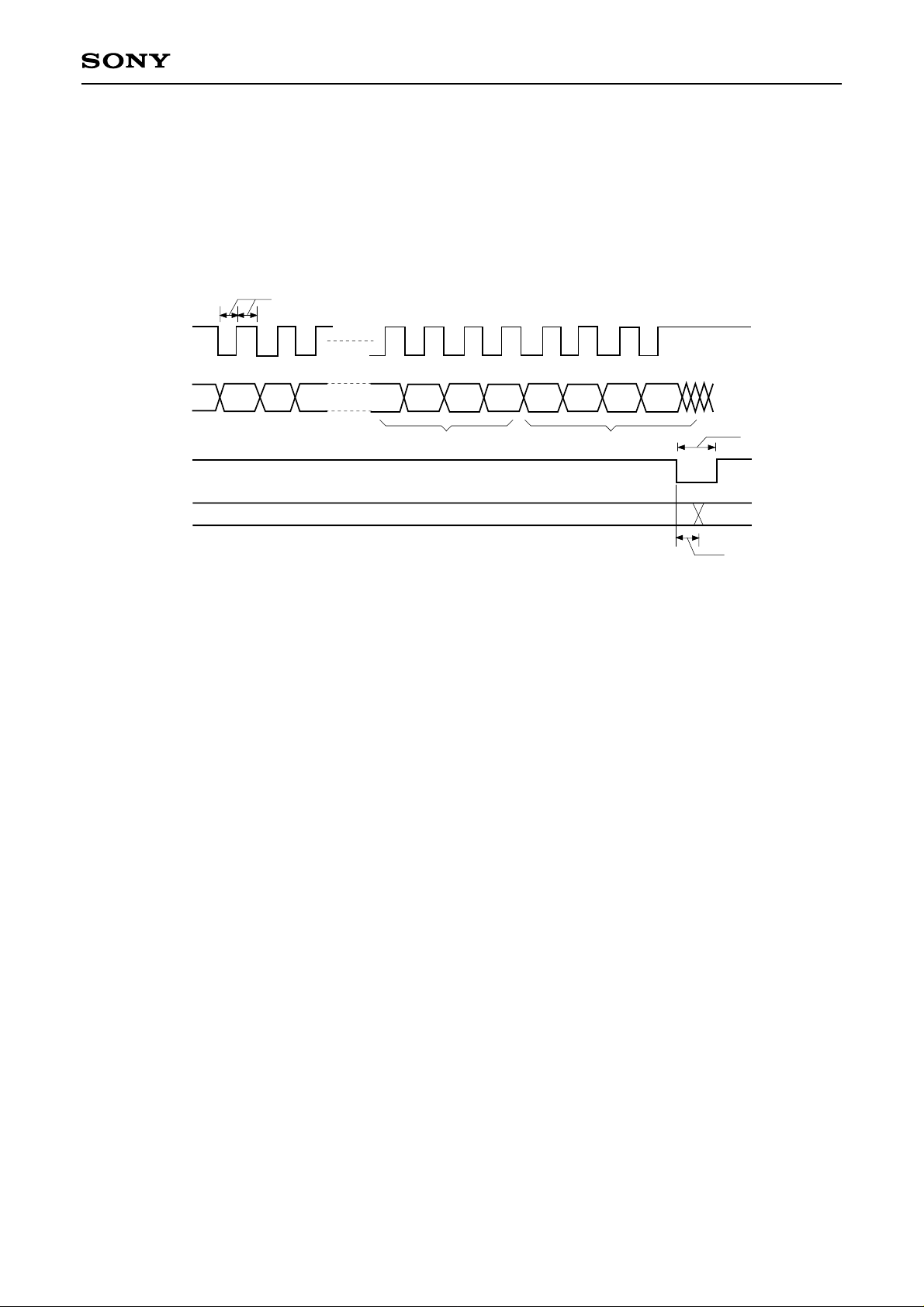
2. CLOK, DATA, XLAT, CNIN, SQCK and EXCK pins
(VDD = AVDD = 5.0V ± 5%, VSS = AVSS = 0V, Topr = –20 to +75°C)
Item Symbol Min. Typ. Max. Unit
CXD2589Q
Clock frequency
Clock pulse width
Setup time
Hold time
Delay time
Latch pulse width
EXCK SQCK frequency
EXCK SQCK pulse width
fCK
tWCK
tSU
tH
tD
tWL
fT
fWT
CLK
DATA
XLT
EXCK
CNIN
SQCK
SQSO
SBSO
750
300
300
300
750
750
tSU
tSU
∗
1/fCK
tWCK tWCK
tH
tWT tWT
1/fT
tH
0.65
0.65
tD
MHz
ns
ns
ns
ns
ns
∗
MHz
ns
tWL
∗
In pseudo double-speed playback mode, except when SQSO is Sub Q Read, the maximum operating
frequency for SQCK is 300kHz and the minimum pulse width is 1.5µs.
3. BCKI, LRCKI and PCMDI pins (VDD = AVDD = 5.0V ± 5%, VSS = AVSS = 0V, Topr = –20 to +75°C)
Item Symbol
BCK pulse width
DATAL, R setup time
DATAL, R hold time
LRCK setup time
BCKI
PCMDI
tW
tSU
tH
tSU
Conditions
tW(BCKI)tW(BCKI)
VDD/2 VDD/2
tSU
(PCMDI)
(PCMDI)
Min.
94
18
18
18
t
H
Typ.
tSU
(LRCKI)
Max. Unit
ns
ns
ns
ns
LRCKI
– 9 –
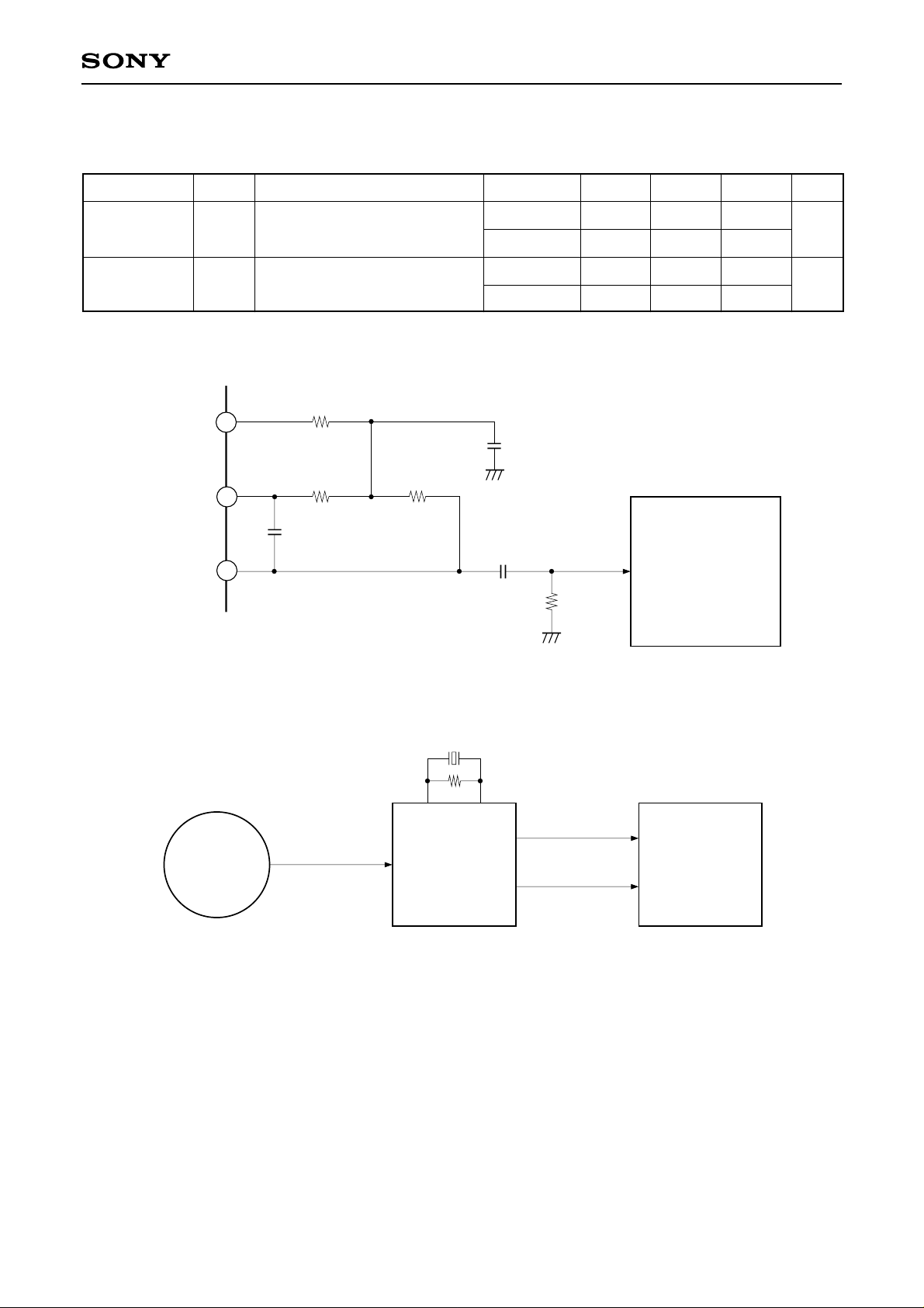
1-bit DAC, LPF Block Analog Characteristics
Analog Characteristics (VDD = AVDD = 5.0V, VSS = AVSS = 0V, Ta = 25°C)
CXD2589Q
Item
Total
harmonic
distortion
S/N ratio
Symbol
THD
S/N
Conditions
1kHz, 0dB data
1kHz, 0dB data
(using A-weighting filter)
Crystal
384Fs
768Fs
384Fs
768Fs
Min.
96
96
For both items, Fs = 44.1kHz.
The total harmonic distortion and S/N ratio measurement circuits are shown below.
150p
12k
12k
680p
12k
22µ
100k
AOUT1 (2)
AIN1 (2)
LOUT1 (2)
Typ.
0.0050
0.0045
Max.
0.0070
0.0065
100
100
SHIBASOKU (AM51A)
Audio Analyzer
Unit
%
dB
TEST DISC
LPF External Circuit Diagram
768Fs/384Fs
Rch A
DATA RF
CXD2589Q
Lch B
Block Diagram for Measuring Analog Characteristics
Audio Analyzer
– 10 –

(VDD = AVDD = 5.0V, VSS = AVSS = 0V, Topr = – 20 to +75°C)
CXD2589Q
Item Symbol
Output voltage
Load resistance
∗
Measured using the circuits on the previous page when a sine wave of 1kHz and 0dB is
VOUT
RL
Min.
8
Typ.
1.12
Max.
∗
Vrms
Applicable pins
Unit
kΩ
output.
Applicable pins
∗1
LOUT1, LOUT2
∗1
∗1
– 11 –
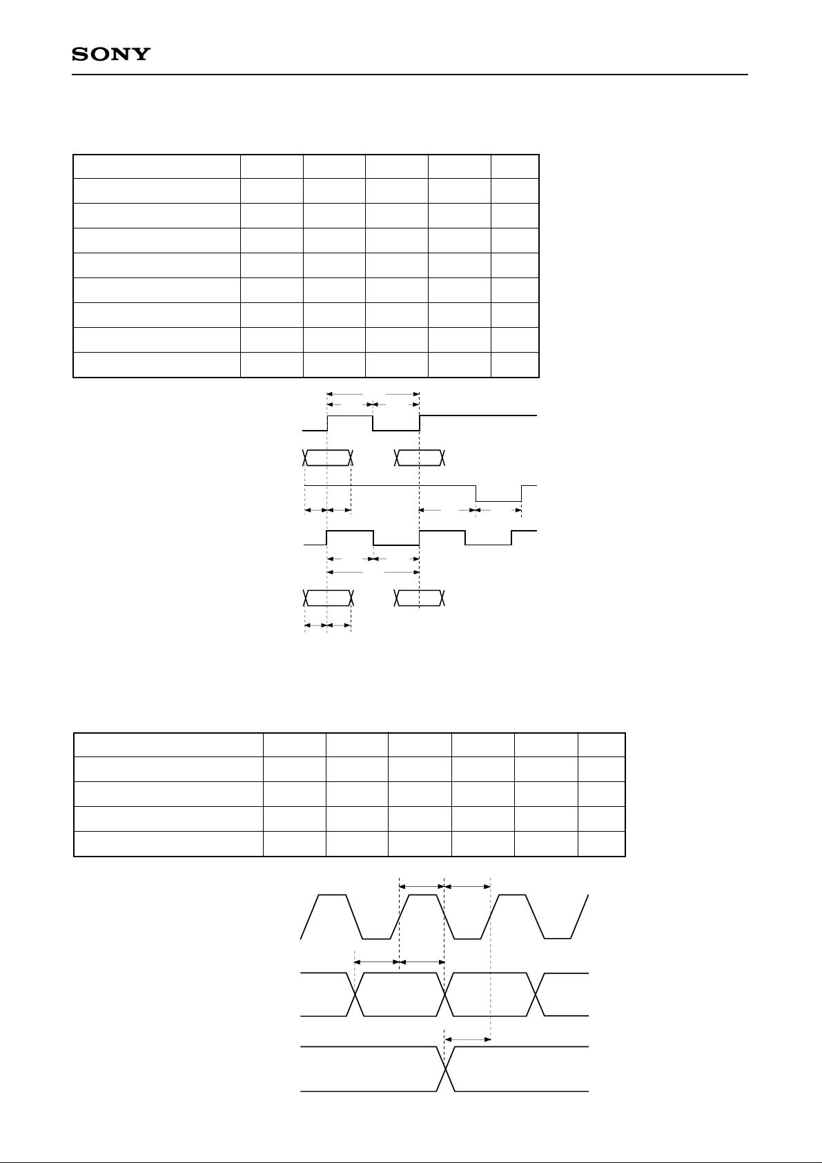
Description of Functions
1. CPU Interface and Commands
• CPU Interface
This interface uses DATA, CLOK and XLAT to set the modes.
The interface timing chart is shown below.
750ns or more
CLOK
CXD2589Q
DATA
XLAT
Registers 4 to E
D1 D2 D3 D0 D1 D2 D3
Data
Address
750ns or more
Valid
300ns max
• Information on each address and the data is provided in Table 1-1.
• The internal registers are initialized by a reset when XRST is low; the initialization data is shown in Table 1-2.
Note) When XLAT is low, SQCK must be set high.
– 12 –
CXD2589Q
Data 6
Data 5
Data 4
Data 3
Data 2
Data 1
D2 D1 D0
D3
D2 D1 D0
D3
D1 D0
D3 D2
D1 D0
D3 D2
D0
D3 D2 D1
D0
D3 D2 D1
—
—
—
—
—
—
—
—
—
—
—
—
—
—
—
—
—
—
—
—
AS0
AS1
AS2
AS3
0
—
—
—
—
—
—
—
—
—
—
—
—
—
—
—
—
—
—
—
—
0.02ms
0.05ms
0.05ms
0.09ms
0.09ms
0.18ms
0.18ms
0.36ms
1
—
—
—
—
—
—
—
—
—
—
—
—
—
—
—
—
—
—
—
—
1.45ms
2.9ms
5.8ms
11.6ms
0
—
—
—
—
—
—
—
—
1
2
4
8
16
32
64
128
256
512
1024
2048
4096
8192
16384
32768
1
—
—
—
—
—
—
—
—
0
1
0
0
KSL0
KSL1
KSL2
KSL3
VCO
SEL2
SOCT
0
VCO
SEL1
WSEL
DOUT
ON/OFF
Mute
DOUT
CDROM
0
—
—
—
—
—
—
—
—
0
—
0
—
—
DCOF
0
—
0
—
0
—
ZMUT
ZMUT
ZDPL
ZDPL
0
0
0
0
MCSL
MCSL
DSPB
ON/OFF
1
SYCOF
0
0
0
0
0
ON/OFF
0
1
OPSL10OPSL1
SYCOF
0
0
0
0
0
DSPB
0
1
—
—
—
—
AD0
AD1
AD2
AD3
OPSL20OPSL2
AD4
AD5
AD6
AD7
AD8
AD9
0
SMUT
EMPH
0
0
ATT
Mute
0
0
0
BBSL
BSBST
LRWO
FMUT
AD0
AD1
AD2
AD3
AD4
AD5
AD6
AD7
AD8
AD9
0
SMUT
EMPH
1
0
0
ATT
Mute
0
0
0
—
—
—
—
—
—
—
—
—
—
—
—
0
0
0
0
MTSL0
MTSL1
TRMO
TRMI
0
CPUSR
SL0
SL1
1
—
—
—
—
—
—
—
—
—
—
—
—
—
—
—
—
—
—
—
—
Gain
Gain
Gain
Gain
0
MDS0
MDS1
MDP0
MDP1
—
—
—
—
—
—
—
—
—
—
—
—
VP0
VP1
VP2
VP3
VP4
VP5
VP6
VP7
Gain
TP
TB
0
1
CLVS
—
—
—
—
—
—
—
—
0
0
Gain
Gain
VPON
LPWR
HIFC
VC2C
SFSL
ICAP
SPDC
EPWM
CM0
CM1
CM2
CM3
0
CAV0
CAV1
Table 1-1
0
Address
Command
Command Table
1
0
D3 D2 D1 D0
Auto sequence
Register name
4
0
1
0
Blind (A, E),
Overflow (C)
Brake (B)
5
1
1
0
Kick (D)
Auto sequence
6
1
1
0
7
0
0
1
(N) track jump
count
MODE
specification
8
0
0
1
Function
9
– 13 –
0
0
1
specification
1
0
1
Audio CTRL
A
1
0
1
1
0
1
Serial bus
CTRL
B
0
1
1
Servo coefficient
C
setting
0
1
1
CLV CTRL
D
1
1
1
CLV mode
E
CXD2589Q
Data 6
Data 5
Data 4
D3 D2 D1 D0
D2 D1 D0
D3
D2 D1 D0
D3
—
—
—
—
—
—
—
—
—
—
—
—
—
—
—
—
—
—
—
—
—
—
—
—
—
—
—
—
—
—
—
—
—
—
—
—
—
—
—
—
—
—
—
—
—
—
—
—
—
—
—
—
—
—
—
0
0
0
0
0
0
—
0
—
0
—
0
—
0
0
1
0
0
0
0
0
0
0
0
—
—
—
0
—
—
—
0
—
—
—
0
—
—
—
0
—
—
—
0
—
—
—
0
—
—
—
0
—
—
—
0
—
—
—
0
—
—
—
0
—
—
—
0
—
—
—
0
0
0
—
—
—
—
—
—
—
—
—
0
0
0
0
0
Data 3
Data 2
Data 1
D2 D1 D0
D3
D1 D0
D3 D2
D1 D0
D3 D2
D0
0
1
—
—
—
—
—
—
—
0
0
0
0
0
0
—
—
—
—
—
—
—
—
—
—
—
—
—
—
1
1
0
1
1
1
0
0
1
0
0
1
0
0
1
0
0
0
0
0
0
0
1
1
0
0
0
0
0
0
0
0
0
0
0
0
0
0
0
0
0
0
0
0
0
0
1
0
0
0
0
0
0
0
0
0
0
0
0
0
1
0
0
1
0
1
1
0
0
0
0
0
1
1
1
0
—
0
—
0
—
0
—
1
—
1
—
1
—
0
0
1
0
1
0
0
0
0
1
0
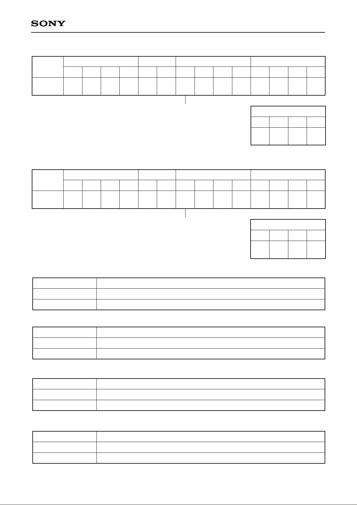
0
0
0
0
0
0
0
0
0
0
0
0
0
1
Table 1-2
Address
Command
Reset Initialization
1
0
D3 D2 D1
Auto sequence
Register name
4
1
0
Blind (A, E),
Overflow (C)
Brake (B)
5
1
0
Kick (D)
Auto sequence
6
1
0
0
1
(N) track jump
count setting
MODE
specification
7
8
0
1
Function
specification
9
– 14 –
0
0
1
1
Audio CTRL
Serial bus
A
B
1
1
CTRL
Servo coefficient
setting
C
1
1
CLV CTRL
D
1
1
CLV mode
E
1-1. The meaning of the data for each address is explained below.
$4X commands
CXD2589Q
Command
CANCEL
FOCUS-ON
1 TRACK JUMP
10 TRACK JUMP
2N TRACK JUMP
N TRACK MOVE
AS3
0
0
1
1
1
1
AS2
0
1
0
0
1
1
AS1
0
1
0
1
0
1
AS0
0
1
RXF
RXF
RXF
RXF
RXF = 0 FORWARD
RXF = 1 REVERSE
• When the Focus-on command ($47) is canceled, $02 is sent and the auto sequence is interrupted.
• When the Track jump/move commands ($48 to $4F) are canceled, $25 is sent and the auto sequence is
interrupted.
$5X commands
Auto sequence timer setting
Setting timers: A, E, C, B
Command
Blind (A, E), Over flow (C)
D3
0.18ms
D2
0.09ms
D1
0.05ms
D0
0.02ms
Brake (B)
0.36ms
0.18ms
Ex.) D2 = D0 = 1, D3 = D1 = 0 (Initial Reset)
A = E = C = 0.11ms
B = 0.23ms
$6X commands
Auto sequence timer setting
Setting timer: D
Command
KICK (D)
D3
11.6ms
D2
5.8ms
Ex.) D3 = 0, D2 = D1 = D0 = 1 (Initial Reset)
D = 10.15ms
$7X commands
Auto sequence track jump/move count setting (N)
Data 1 Data 2
Command
D3 D2 D1 D0 D3 D2 D1 D0 D3 D2 D1 D0 D3 D2 D1 D0
Auto sequence track jump
count setting
2152142132122112102928272625242322212
0.09ms
D1
2.9ms
0.05ms
D0
1.45ms
Data 3 Data 4
0
This command is used to set N when a 2N-track jump and an N-track move are executed for auto sequence.
• The maximum track count is 65,535, but note that with 2N-track jumps the maximum track jump count is
determined by the mechanical limitations of the optical system.
• The number of tracks jumped is counted according to the signals input from the CNIN pin.
– 15 –
$8X commands
CXD2589Q
Command
MODE
specification
Command bit
CDROM = 1
CDROM = 0
Data 1
D3
CDROM
D2 D1 D0 D3 D2 D1 D0 D3 D2 D1 D0
DOUT
Mute
DOUT
ON/OFF
WSEL
Data 4
D3
D2 D1 D0
0010
C2PO timing
See Timing Chart
1-1.
See Timing Chart
1-1.
VCO
SEL1
Data 2
0
SOCT
VCO
SEL2
KSL3 KSL2 KSL1 KSL0
Data 3
See the $BX commands.
Processing
CDROM mode; average value interpolation and pre-value hold
are not performed.
Audio mode; average value interpolation and pre-value hold
are performed.
Command bit
DOUT Mute = 1
DOUT Mute = 0
Digital Out output is muted. (DA output is not muted.)
When no other mute conditions are set, Digital Out output is not muted.
Command bit
DOUT ON/OFF = 1
DOUT ON/OFF = 0
Command bit
WSEL = 1
WSEL = 0
∗
1
In normal-speed playback, channel clock = 4.3218MHz.
Digital Out is output from the DOUT pin.
Digital Out is not output from the DOUT pin.
Sync protection window width
±26 channel clock
∗1
±6 channel clock
Processing
Processing
Application
Anti-rolling is enhanced.
Sync window protection is enhanced.
– 16 –
CXD2589Q
Command bit
VCOSEL1
0
0
0
0
1
1
1
1
∗1
Approximately twice the normal speed.
KSL3 KSL2
0
0
1
1
0
0
1
1
0
1
0
1
0
1
0
1
Processing
Multiplier PLL VCO1 is set to normal speed, and the output is 1/1
frequency-divided.
Multiplier PLL VCO1 is set to normal speed, and the output is 1/2
frequency-divided.
Multiplier PLL VCO1 is set to normal speed, and the output is 1/4
frequency-divided.
Multiplier PLL VCO1 is set to normal speed, and the output is 1/8
frequency-divided.
Multiplier PLL VCO1 is set to high speed∗1, and the output is 1/1
frequency-divided.
Multiplier PLL VCO1 is set to high speed∗1, and the output is 1/2
frequency-divided.
Multiplier PLL VCO1 is set to high speed∗1, and the output is 1/4
frequency-divided.
Multiplier PLL VCO1 is set to high speed∗1, and the output is 1/8
frequency-divided.
Command bit
VCOSEL2
0
0
0
0
1
1
1
1
∗2
Approximately twice the normal speed.
KSL1 KSL0
0
0
1
1
0
0
1
1
0
1
0
1
0
1
0
1
Processing
Wide-band PLL VCO2 is set to normal speed, and the output is 1/1
frequency-divided.
Wide-band PLL VCO2 is set to normal speed, and the output is 1/2
frequency-divided.
Wide-band PLL VCO2 is set to normal speed, and the output is 1/4
frequency-divided.
Wide-band PLL VCO2 is set to normal speed, and the output is 1/8
frequency-divided.
Wide-band PLL VCO2 is set to high speed∗2, and the output is 1/1
frequency-divided.
Wide-band PLL VCO2 is set to high speed∗2, and the output is 1/2
frequency-divided.
Wide-band PLL VCO2 is set to high speed∗2, and the output is 1/4
frequency-divided.
Wide-band PLL VCO2 is set to high speed∗2, and the output is 1/8
frequency-divided.
– 17 –

If C2 Pointer = 1,
data is NG
CXD2589Q
Rch 16bit C2 Pointer Lch 16bit C2 Pointer
Lch C2 Pointer
C2 Pointer for upper 8bits C2 Pointer for lower 8bits
Rch C2 Pointer
C2 Pointer for upper 8bits C2 Pointer for lower 8bits
Timing Chart 1-1
LRCK
C2PO
CDROM = 0
– 18 –
C2PO
CDROM = 1
CXD2589Q
$9X commands (OPSL1= 0)
Data 1
Command
D3
Function
specification
D2 D1 D0 D3
DSPB
0
ON/OFF
$9X commands (OPSL1= 1)
Data 1
Command
D3
Function
specification
D2 D1 D0 D3 D2 D1 D0 D3 D2 D1 D0
DSPB
0
ON/OFF
∗
Data 2 D0 and subsequent data are DF/DAC function settings.
Data 2
D3 to D1
0
0 0 MCSL 0 0
000
D0
SYCOF
Data 3
D2
D1 D0 D3 D2 D1 D0
ZDPL
OPSL1
D3
—
∗
Data 2 D0 and subsequent data are DF/DAC function settings.
Data 3
D3 to D1
0
000
0
D0
SYCOF
1 MCSL 0 0 ZDPL ZMUT 0 0
OPSL1
Data 4
ZMUT — —
Data 5
D2 D1 D0
———
Data 4Data 2
Data 5
Command bit
DSPB = 1
DSPB = 0
Double-speed playback (CD-DSP block)
Normal-speed playback (CD-DSP block)
Command bit
SYCOF = 1
SYCOF = 0
∗
Set SYCOF = 0 in advance when setting the $AX command LRWO to 1.
LRCK asynchronous mode
Normal operation
Command bit
OPSL1 = 1
OPSL1 = 0
DCOF can be set.
DCOF cannot be set.
Processing
Processing
Processing
D3
D2 D1 D0
0 DCOF 0 0
Command bit
MCSL = 1
MCSL = 0
Processing
DF/DAC block master clock selection. Crystal = 768Fs (33.8688MHz)
DF/DAC block master clock selection. Crystal = 384Fs (16.9344MHz)
– 19 –
 Loading...