

Sony CXD2498R Datasheet

CXD2498R
Timing Generator for Frame Readout CCD Image Sensor
Description
The CXD2498R is a timing generator IC which
generates the timing pulses for performing frame
readout using the ICX282 CCD image sensor.
Features
• Base oscillation frequency 45MHz
• Electronic shutter function
• Supports various drive modes such as draft and
AF mode
• Horizontal driver for CCD image sensor
• Vertical driver for CCD image sensor
Applications
Digital still cameras
Structure
Silicon gate CMOS IC
Applicable CCD Image Sensors
ICX282 (Type 2/3, 5070K pixels)
Absolute Maximum Ratings
• Supply voltage VDD VSS – 0.3 to +7.0 V
• Input voltage VI VSS – 0.3 to VDD + 0.3 V
• Output voltage VO1 VSS – 0.3 to VDD + 0.3 V
• Operating temperature
• Storage temperature
48 pin LQFP (Plastic)
VL –10.0 to VSS V
VH VL – 0.3 to +26.0 V
VO2 VL – 0.3 to VSS + 0.3 V
VO3 VL – 0.3 to VH + 0.3 V
Topr –20 to +75 °C
Tstg –55 to +150 °C
Recommended Operating Conditions
• Supply voltage
VDDa, VDDb, VDDc 3.0 to 3.6 V
VM 0.0 V
VH 14.5 to 15.5 V
VL –7.0 to –8.0 V
• Operating temperature
Topr –20 to +75 °C
Sony reserves the right to change products and specifications without prior notice. This information does not convey any license by
any implication or otherwise under any patents or other right. Application circuits shown, if any, are typical examples illustrating the
operation of the devices. Sony cannot assume responsibility for any problems arising out of the use of these circuits.
– 1 –
E00X63-PS
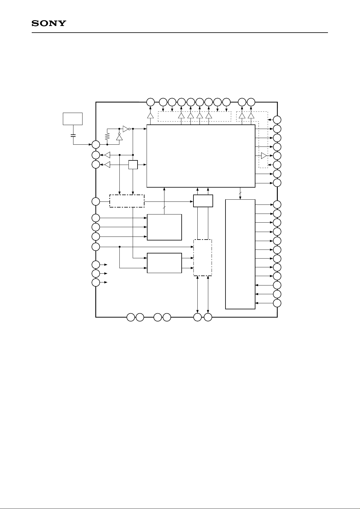
Block Diagram
CXD2498R
VCO
SNCSL
SSGSL
CKI
CKO
MCKO
SSI
SCK
SEN
RST
TEST1
TEST2
26
25
30
31
32
33
27
28
H2B
H2A
15
Selector
SS2
V
VSS3
9
14
V Driver
XSHP
1918
XSHD
17
20
21
22
23
24
4
5
40
42
43
38
44
46
47
39
48
41
37
45
DD4
V
PBLK
CLPDM
OBCLP
ADCLK
SS4
V
ID/EXP
WEN
V1A
V1B
V1C
V2
V3A
V3B
V3C
V4
SUB
VH
VM
VL
11
DD3VDD2
V
H1A
121016
H1B
13
RG
8
Pulse Generator
1/2
3
Selector
Latch
Register
6
2
SSG
7 29 1
DD5VDD1
V
VSS136VSS5
– 2 –
35 34
HD
VD
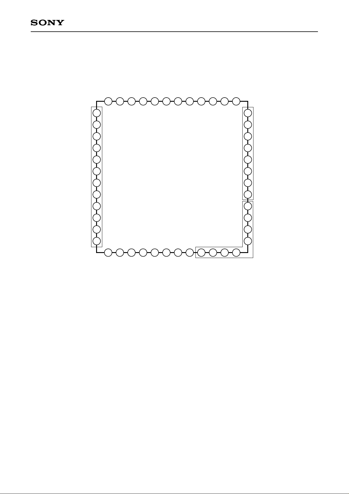
Pin Configuration
CXD2498R
VM
V2
V4
V1A
VH
V1B
V1C
V3A
VL
V3B
V3C
SUB
36
SS5
HD
V
VD
SEN
35
323334
SCK
SSI
31
30
DD5
TEST2
V
MCKO
29
37
38
39
40
41
42
43
44
45
46
47
48
1 2 3 4 5 6 7 8 9 10 11 12
TEST1
262728
CKI
25
CKO
SS4
V
24
ADCLK
23
OBCLP
22
CLPDM
21
PBLK
20
XSHD
19
XSHP
18
V
DD4
17
V
DD3
16
H2B
15
14
SS3
V
13
H2A
RG
SS1
RST
V
SNCSL
∗
Groups of pins enclosed in the figure indicate sections for which power supply separation is possible.
ID/EXP
WEN
SSGSL
DD1
V
SS2
V
H1A
DD2
H1B
V
– 3 –
Pin Description
CXD2498R
Pin
No.
1
2
3
4
5
6
7
8
9
10
11
12
13
Symbol I/O Description
VSS1
RST
SNCSL
—
GND
Internal system reset input. High: Normal operation, Low: Reset control
I
Normally apply reset during power-on. Schmitt trigger input
Control input used to switch sync system. High: CKI sync, Low: MCKO sync
I
Vertical direction line identification pulse output/exposure time identification pulse
ID/EXP
O
output.
Switching possible using the serial interface data. (Default: ID)
WEN
SSGSL
VDD1
RG
VSS2
H1A
VDD2
H1B
H2A
O
Memory write timing pulse output.
Internal SSG enable. High: Internal SSG valid, Low: External sync valid
I
—
3.3V power supply. (Power supply for common logic block)
O
CCD reset gate pulse output.
—
GND
O
CCD horizontal register clock output.
—
3.3V power supply. (Power supply for H block)
O
CCD horizontal register clock output.
O
CCD horizontal register clock output.
With pull-down resistor
With pull-down resistor
14
15
16
17
18
19
20
21
22
23
24
25
26
27
28
29
VSS3
H2B
VDD3
VDD4
XSHP
XSHD
PBLK
CLPDM
OBCLP
ADCLK
VSS4
CKO
CKI
TEST1
TEST2
VDD5
—
GND
O
CCD horizontal register clock output.
—
3.3V power supply. (Power supply for H block)
—
3.3V power supply. (Power supply for CDS block)
O
CCD precharge level sample-and-hold pulse output.
O
CCD data level sample-and-hold pulse output.
O
Pulse output for horizontal and vertical blanking period pulse cleaning.
O
CCD dummy signal clamp pulse output.
CCD optical black signal clamp pulse output.
O
The horizontal OB pattern can be changed using the serial interface data.
Clock output for analog/digital conversion IC.
O
Logical phase adjustment possible using the serial interface data.
—
GND
O
Inverter output.
I
Inverter input.
I
IC test pin 1; normally fixed to GND. With pull-down resistor
I
IC test pin 2; normally fixed to GND. With pull-down resistor
—
3.3V power supply. (Power supply for common logic block)
30
31
MCKO
SSI
O
System clock output for signal processing IC.
Serial interface data input for internal mode settings.
I
– 4 –
Schmitt trigger input
CXD2498R
Pin
No.
32
33
34
35
36
37
38
39
40
41
42
43
44
45
46
47
48
Symbol I/O Description
SCK
SEN
VD
HD
V
SS5
VM
V2
V4
V1A
VH
V1B
V1C
V3A
VL
V3B
V3C
SUB
Serial interface clock input for inter nal mode settings.
I
Serial interface strobe input for internal mode settings.
I
Vertical sync signal input/output.
I/O
Horizontal sync signal input/output.
I/O
GND
—
GND (GND for vertical driver)
—
CCD vertical register clock output.
O
CCD vertical register clock output.
O
CCD vertical register clock output.
O
15.0V power supply. (Power supply for vertical driver)
—
CCD vertical register clock output.
O
CCD vertical register clock output.
O
CCD vertical register clock output.
O
–7.5V power supply. (Power supply for vertical driver)
—
CCD vertical register clock output.
O
CCD vertical register clock output.
O
CCD electronic shutter pulse output.
O
Schmitt trigger input
Schmitt trigger input
– 5 –
CXD2498R
Electrical Characteristics
DC Characteristics (Within the recommended operating conditions)
Item
Supply
voltage 1
Supply
voltage 2
Supply
voltage 3
Input voltage
∗1
1
Input voltage
∗2
2
Input/output
voltage
Output
voltage 1
Output
voltage 2
Output
voltage 3
Pins
VDD2, VDD3
VDD4
VDD1, VDD5
RST, SSI,
SCK, SEN
TEST1, TEST2,
SNCSL, SSGSL
VD, HD
H1A, H1B,
H2A, H2B
RG
XSHP, XSHD,
PBLK, OBCLP,
CLPDM, ADCLK
Symbol
VDDa
VDDb
VDDc
Vt+
Vt–
VIH1
VIL1
VIH2
VIL2
VOH1
VOL1
VOH2
VOL2
VOH3
VOL3
VOH4
VOL4
Conditions Min. Max. Unit
Feed current where IOH = –1.2mA
Pull-in current where IOL = 2.4mA
Feed current where IOH = –22.0mA
Pull-in current where IOL = 14.4mA
Feed current where IOH = –3.3mA
Pull-in current where IOL = 2.4 mA
Feed current where IOH = –3.3mA
Pull-in current where IOL = 2.4mA
3.0
3.0
3.0
0.8VDDc
0.7VDDc
0.8VDDc
VDDc – 0.8
VDDa – 0.8
VDDc – 0.8
VDDb – 0.8
Typ.
3.3
3.3
3.3
3.6
3.6
3.6
0.2VDDc
0.2VDDc
0.2VDDc
0.4
0.4
0.4
0.4
V
V
V
V
V
V
V
V
V
V
V
V
V
V
V
V
V
Output
voltage 4
Output
voltage 5
Output
voltage 6
CKO
MCKO
ID/EXP, WEN
VOH5
VOL5
VOH6
VOL6
VOH7
VOL7
IOL
Output
current 1
V1A, V1B, V1C,
V3A, V3B, V3C,
V2, V4
IOM1
IOM2
IOH
Output
current 2
∗1
This input pin is a schmitt trigger input.
∗2
This input pin is with pull-down registor in the IC.
SUB
IOSL
IOSH
Feed current where IOH = –6.9mA
Pull-in current where IOL = 4.8mA
Feed current where IOH = –3.3mA
Pull-in current where IOL = 2.4mA
Feed current where IOH = –2.4mA
Pull-in current where IOL = 4.8mA
V1A/B/C, V2, V3A/B/C ,
V4 = –8.25V
V1A/B/C, V2, V3A/B/C ,
V4 = –0.25V
V1A/B/C, V3A/B/C = 0.25V
V1A/B/C, V3A/B/C = 14.75V
SUB = –8.25V
SUB = 14.75V
– 6 –
VDDc – 0.8
VDDc – 0.8
VDDc – 0.8
10.0
5.0
5.4
0.4
0.4
0.4
–5.0
–7.2
–4.0
V
V
V
V
V
V
mA
mA
mA
mA
mA
mA
Inverter Input Characteristics for Base Oscillation Clock Duty Adjustment
(Within the recommended operating conditions)
CXD2498R
Item Pins
Logical Vth
Input voltage
Input amplitude
CKI
Symbol
Conditions
LVth
VIH
VIL
VIN fmax = 50MHz sine wave
Min. Typ. Max. Unit
VDDc/2
0.7VDDc
0.3VDDc
0.3
V
V
V
Vp-p
Note) Input voltage is the input voltage characteristics for direct input from an external source.
Input amplitude is the input amplitude characteristics in the case of input through a capacitor.
Switching Characteristics (VH = 15.0V, VM = GND, VL = –7.5V)
Item Symbol
Rise time
Fall time
Output noise
voltage
TTLM
TTMH
TTLH
TTML
TTHM
TTHL
VCLH
VCLL
VCMH
VCML
Conditions
VL to VM
VM to VH
VL to VH
VM to VL
VH to VM
VH to VL
Min. Typ. Max. Unit
200
200
30
200
200
30
350
350
60
350
350
60
500
500
90
500
500
90
1.0
1.0
1.0
1.0
ns
ns
ns
ns
ns
ns
V
V
V
V
Note)
1) The MOS structure of this IC has a low tolerance for static electr icity, so full care should be given for
measures to prevent electrostatic discharge.
2) For noise and latch-up counter measures, be sure to connect a by-pass capacitor (0.1µF or more)
between each power supply pin (VH, VL) and GND.
3) To protect the CCD image sensor, clamp the SUB pin output at VH before input to the CCD image
sensor.
– 7 –
Switching Wa veforms
CXD2498R
V1A (V1B, V1C, V3A, V3B, V3C)
V2 (V4)
TTLM
10%
TTLM
10%
TTMH TTHM
90%
10%
90%
90%
TTLH TTHL
90%
10%
90%
90%
90%90%
TTML
10%
TTML
10%
VH
VM
VL
VM
VL
VH
Waveform Noise
SUB
VCLH
10% 10%
VCMH
VCML
VCLL
VL
VM
VL
– 8 –
Measurement Circuit
CXD2498R
Serial interface data
VD
HD
+3.3V
–7.5V
+15.0V
R1
C2
C1
C2
C1
C1
C2
C2
C2
C2
R1
R1 R1
C2 C2
R1
C2
C1
C2
C2
C2
C1
C2
C2
C1
C2
R2
R1
C3
30
29
35
36
37
38
39
40
41
42
43
44
45
46
47
48
1 2 3 4 5 6 7 8 9 10 11 12
31
323334
CXD2498R
CKI
C6
C6
25
262728
24
23
22
21
20
19
18
17
16
15
14
13
C5
C5C4
C6
C6
C6
C6
C6
C6
C5
C5
C1: 3300pF C2: 560pF C3: 820pF C4: 8pF C5: 320pF C6: 10pF
R1: 30Ω R2: 10Ω
– 9 –
AC Characteristics
AC characteristics between the serial interface clocks
CXD2498R
0.8VDDc
th1ts1
ts2
Symbol
ts1
th1
ts2
ts3
SSI
SCK
SEN
SEN
0.2V
0.2VDDc
DD
c
0.8VDDc
ts3
Definition Min. Typ. Max. Unit
SSI setup time, activated by the rising edge of SCK
SSI hold time, activated by the rising edge of SCK
SCK setup time, activated by the rising edge of SEN
SEN setup time, activated by the rising edge of SCK
Serial interface clock internal loading characteristics (1)
DD
c
0.8V
(Within the recommended operating conditions)
20
20
20
20
Example: During frame mode
ns
ns
ns
ns
VD
HD
V1A
Enlarged view
HD
V1A
SEN
∗
Be sure to maintain a constantly high SEN logic level near the falling edge of the HD in the horizontal period
0.8V
DDc
0.2V
DDc
ts1
th1
0.2V
DDc
during which V1A/B/C and V3A/B/C values take the ternary value and during that horizontal period.
(Within the recommended operating conditions)
Symbol
ts1
th1
SEN setup time, activated by the falling edge of HD
SEN hold time, activated by the falling edge of HD
Definition Min. Typ. Max. Unit
0
134
ns
µs
∗
Restriction in draft mode with an operating frequency of 22.5MHz.
– 10 –
Serial interface clock internal loading characteristics (2)
VD
HD
Enlarged view
CXD2498R
Example: During frame mode
VD
HD
SEN
∗
Be sure to maintain a constantly high SEN logic level near the falling edge of VD.
0.8V
DD
c
0.2V
DD
ts1
c
th1
DD
c
0.2V
(Within the recommended operating conditions)
Symbol
SEN setup time, activated by the falling edge of VD
ts1
SEN hold time, activated by the falling edge of VD
th1
∗
Restriction with an operating frequency of 22.5MHz.
Definition Min. Typ. Max. Unit
0
200
ns
ns
Serial interface clock output variation characteristics
Normally, the ser ial interface data is loaded to the CXD2498R at the timing shown in “Serial interface clock
internal loading characteristics (1)” above. However, one exception to this is when the data such as STB is
loaded to the CXD2498R and controlled at the rising edge of SEN. See ”Description of Operation”.
SEN
Output signal
0.8VDDc
tpdPULSE
(Within the recommended operating conditions)
Symbol Definition Min. Typ. Max. Uniy
tpdPULSE
Output signal delay, activated by the rising edge of SEN 5 ns
70
– 11 –
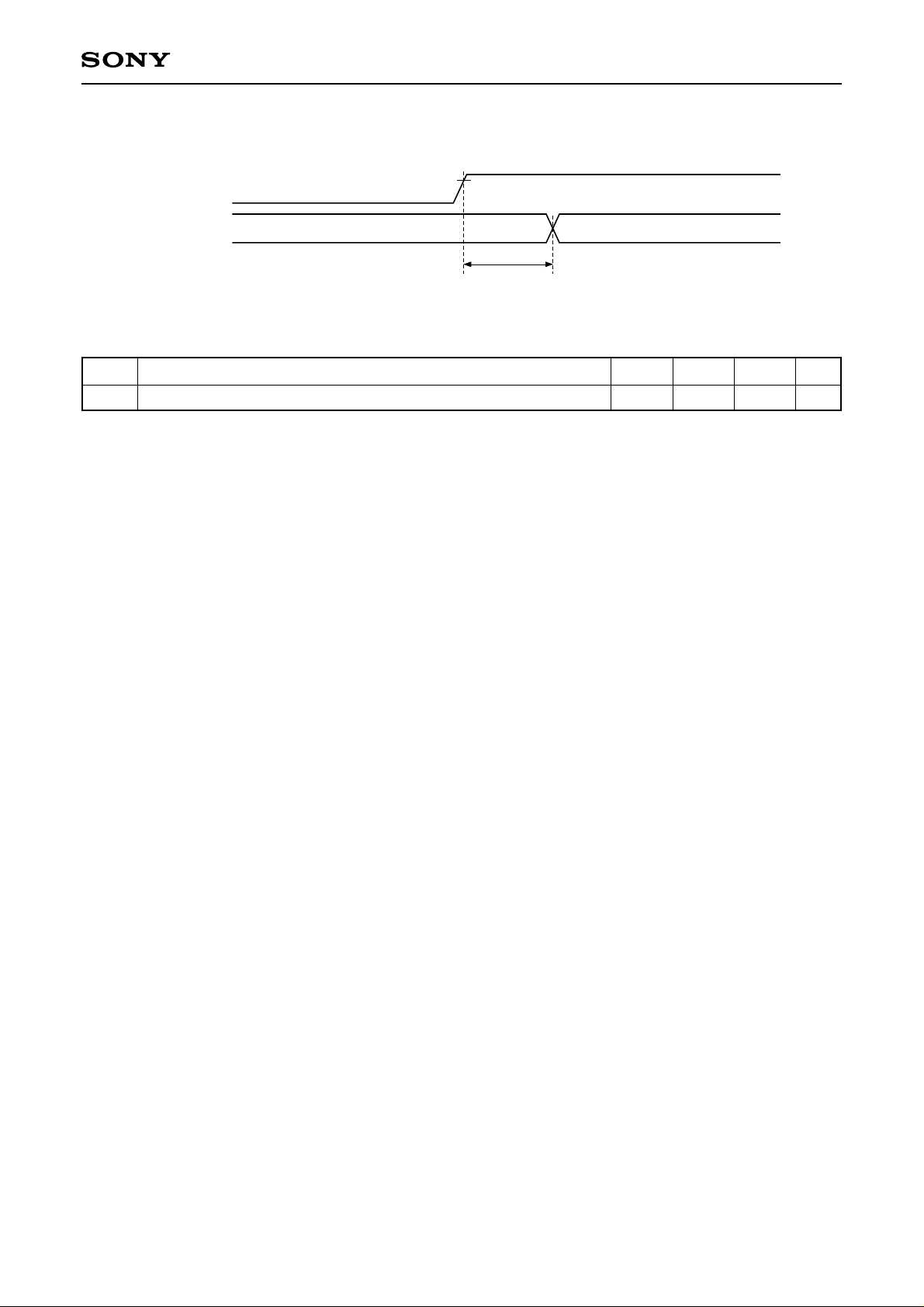
RST loading characteristics
CXD2498R
RST
Symbol
tw1
RST pulse width ns
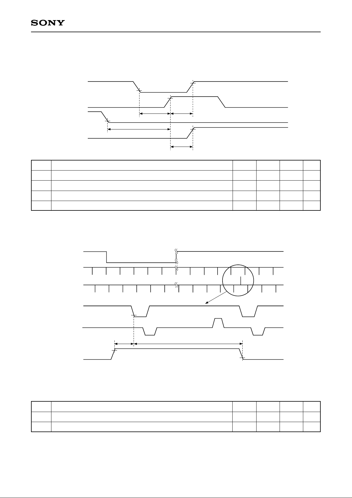
VD and HD phase characteristics
VD
HD
Symbol
VD setup time, activated by the falling edge of HD
ts1
VD hold time, activated by the falling edge of HD
th1
0.2VDDc
tw1
0.8VDDc
(Within the recommended operating conditions)
Definition Min. Typ. Max. Unit
22
0.2V
DD
0.2V
DD
c
ts1
0.2V
DD
th1
c
c
(Within the recommended operating conditions)
Definition Min. Typ. Max. Unit
0ns
ns44
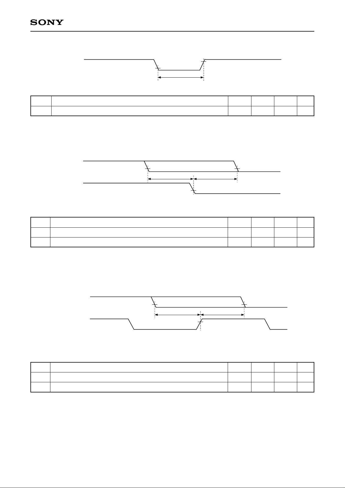
HD loading characteristics
HD
MCKO
MCKO load capacitance = 10pF
Symbol
HD setup time, activated by the rising edge of MCKO
ts1
HD hold time, activated by the r ising edge of MCKO
th1
DD
d
0.2V
DD
d
ts1
0.8V
DD
th1
d
0.2V
(Within the recommended operating conditions)
Definition Min. Typ. Max. Unit
31
0
ns
ns
– 12 –
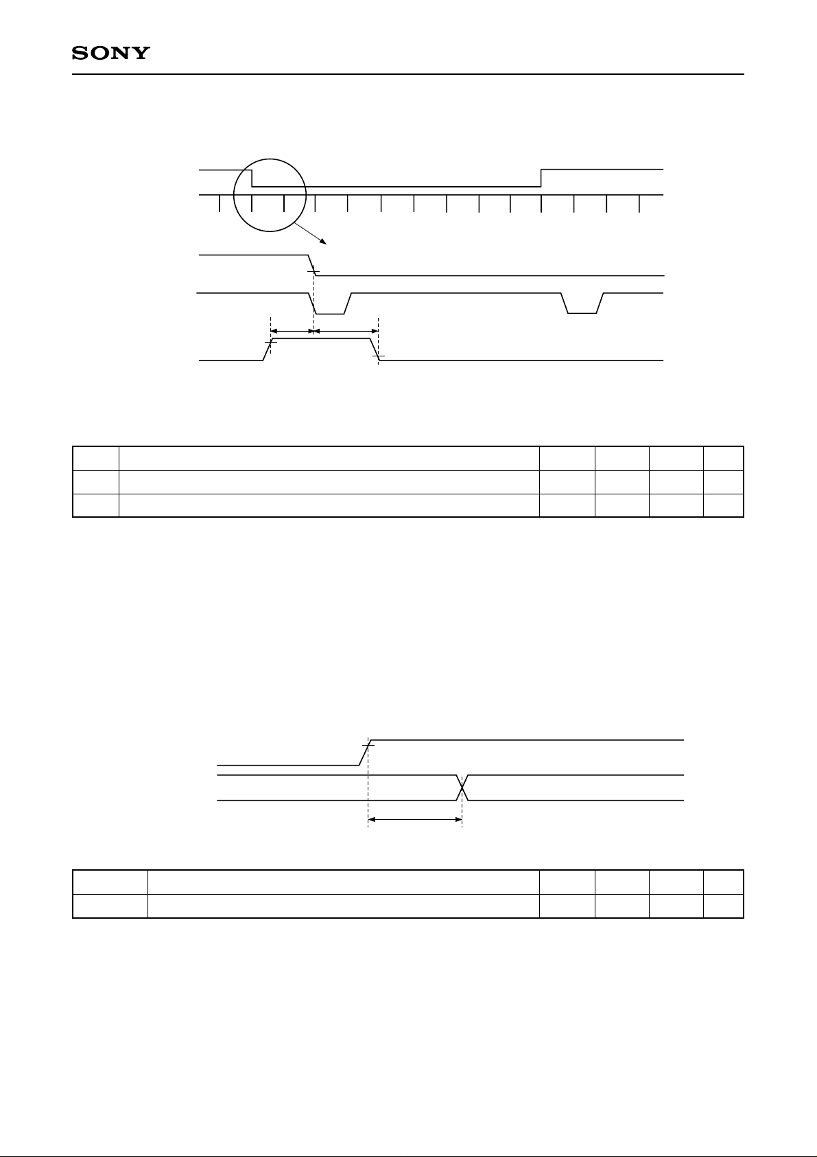
Output variation characteristics
CXD2498R
MCKO
WEN, ID/EXP
WEN and ID/EXP load capacitance = 10pF
Symbol
tpd1
Time until the above outputs change after the rise of MCKO ns23 33
Definition Min. Typ. Max. Unit
0.8VDDc
tpd1
(Within the recommended operating conditions)
– 13 –
CXD2498R
Description of Operation
Pulses output from the CXD2498R are controlled mainly by the RST pin and by the serial interface data. The
Pin Status Table is shown below, and the details of serial interface control are described on the following
pages.
Pin Status Table
Pin
Symbol CAM SLP STB RST
No.
1
2
3
4
5
6
7
8
9
10
11
12
13
14
15
16
17
18
19
20
21
22
23
24
VSS1
RST
SNCSL
ID/EXP
WEN
SSGSL
VDD1
RG
VSS2
H1A
VDD2
H1B
H2A
VSS3
H2B
VDD3
VDD4
XSHP
XSHD
PBLK
CLPDM
OBCLP
ADCLK
VSS4
ACT ACT ACT L
ACT ACT ACT ACT
ACT L L L
ACT L L L
ACT ACT ACT ACT
ACT L L ACT
ACT L L ACT
ACT L L ACT
ACT L L ACT
ACT L L ACT
ACT L L ACT
ACT L L ACT
ACT L L H
ACT L L H
ACT L L H
ACT L L ACT
—
—
—
—
—
—
—
—
Pin
Symbol CAM SLP STB RST
No.
25
26
27
28
29
30
31
32
33
34
35
36
37
38
39
40
41
42
43
44
45
46
47
48
CKO
CKI
TEST1
TEST2
VDD5
MCKO
SSI
SCK
SEN
∗1
VD
∗1
HD
VSS5
VM
V2
V4
V1A
VH
V1B
V1C
V3A
VL
V3B
V3C
SUB
ACT ACT L ACT
ACT ACT ACT ACT
—
—
—
ACT ACT L ACT
ACT ACT ACT DIS
ACT ACT ACT DIS
ACT ACT ACT DIS
ACT L L H
ACT L L H
—
—
ACT VM VM VM
ACTVMVMVL
ACT VH VH VM
—
ACT VH VH VM
ACT VH VH VM
ACT VH VH VL
—
ACT VH VH VL
ACT VH VH VL
ACT VH VH VL
∗1
It is for output. For input, all items are “ACT”.
Note) ACT means that the circuit is operating, and DIS means that loading is stopped. L indicates a low
output level, and H a high output level in the controlled status.
Also, VH, VM and VL indicate the voltage levels applied to VH (Pin 41), VM (Pin 37) and VL (Pin 45),
respectively, in the controlled status.
– 14 –
CXD2498R
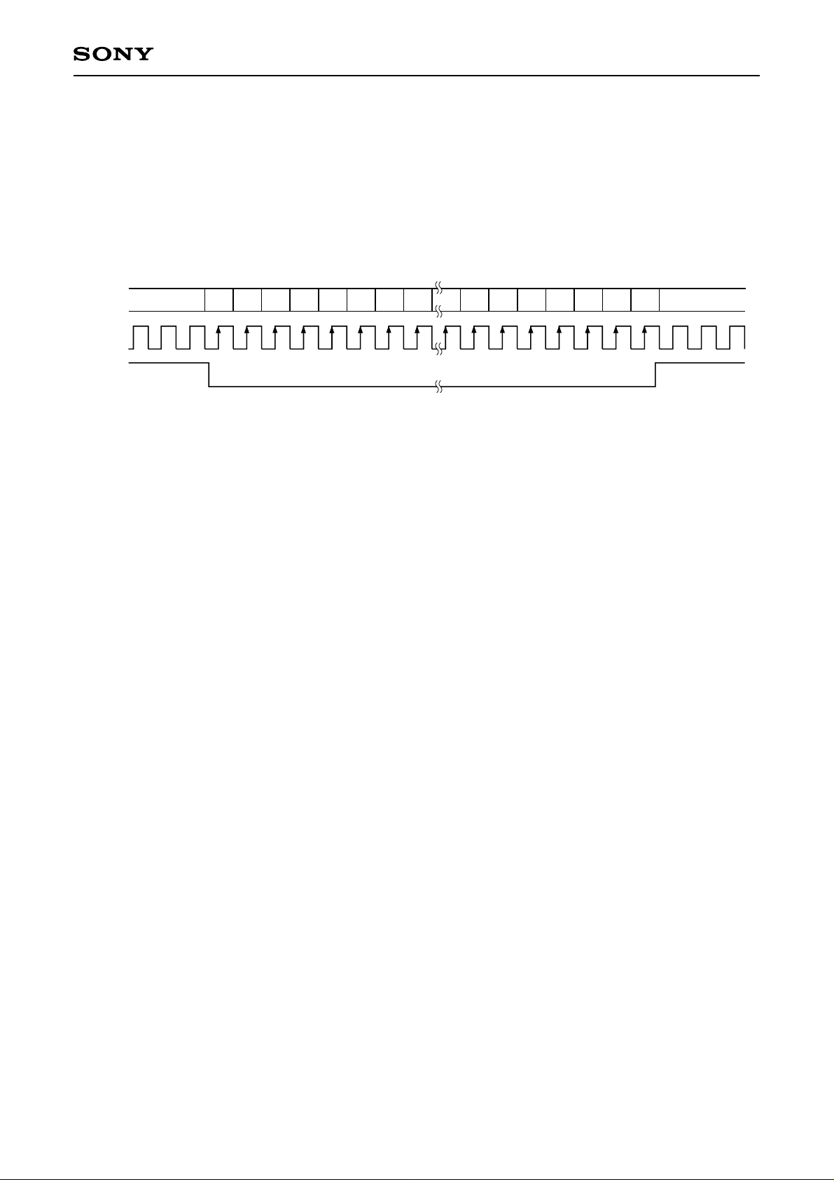
Serial Interface Control
The CXD2498R basically loads and reflects the serial interface data sent in the following format in the readout
portion at the falling edge of HD. Here, readout portion specifies the horizontal period dur ing which V1A/B/C
and V3A/B/C, etc. take the ternary value.
Note that some items reflect the serial interface data at the falling edge of VD or the rising edge of SEN.
SSI
SCK
SEN
00 01 02 03 04 05 06 07 41 42 43 44 45 46 47
These are two categories of serial interface data : the CXD2498R dr ive control data (hereafter “control data”)
and electronic shutter data (hereafter “shutter data”).
The details of each data are described below.
– 15 –
CXD2498R
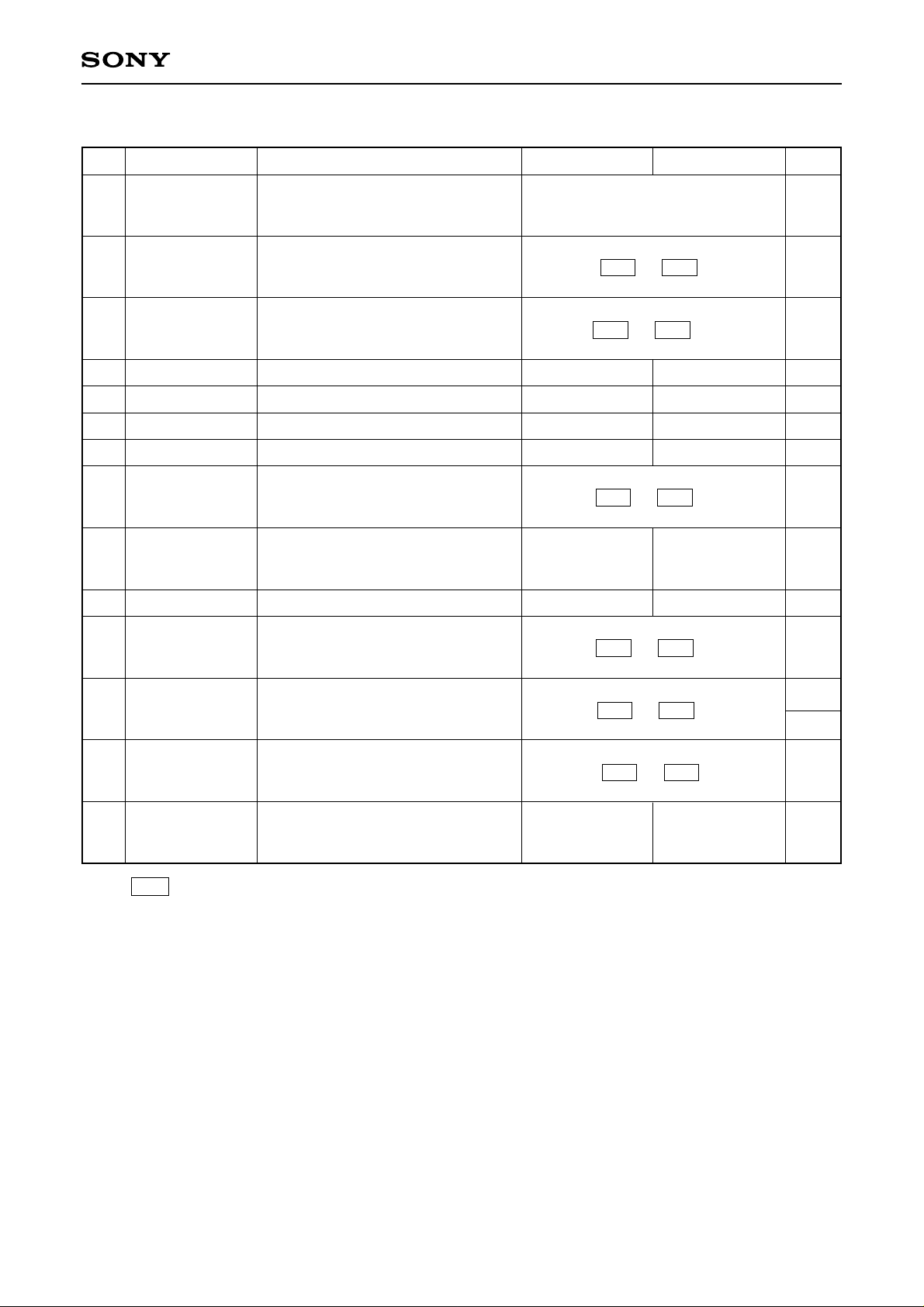
Control Data
Data Symbol Function Data = 0 Data = 1 RST
D00
to
D07
D08
to
D09
D10
to
D11
D12
D13
D14
D15
D16
to
D17
D18
to
D32
D33
D34
to
D35
D36
to
D37
CHIP
CTG
MODE
SMD
HTSG
PTMD
EXP
PTOB
LDAD
—
—
—
Chip enable
Category switching
Drive mode switching
—
Electronic shutter mode switching
HTSG control switching
∗1
∗1
—
Drive mode pattern switching
—
ID/EXP output switching
OBCLP waveform pattern switching
ADCLK logic phase adjustment
10000001 → Enabled
Other values → Disabled
See D08 to D09 CTG.
See D10 to D11 MODE.
——
OFF ON
OFF ON
——
See D16 to D17 PTMD.
——
ID EXP
See D34 to D35 PTOB.
See D36 to D37 LDAD.
All
0
All
0
All
0
0
0
0
0
All
0
All
0
0
All
0
1
0
D38
to
STB
D39
D40
to
D47
∗1
See D13 SMD.
—
Standby control
—
– 16 –
See D38 to D39 STB.
——
All
All
0
0
 Loading...