

Sony CXD2475TQ Datasheet
Reference Voltage and Driver IC for LCD
Description
The CXD2475TQ is suitable IC for applying reference
voltage for gamma correction which is necessary for
TFT liquid crystal display. This IC has a built-in 9
channels of rail-to-rail buffer circuit which enables 2input switch and a common driver circuit.
Features
• Built-in 9 channels of rail-to-rail buffer circuit
• Built-in common driver circuit
• Current consumption: 3.6mA (typ.)
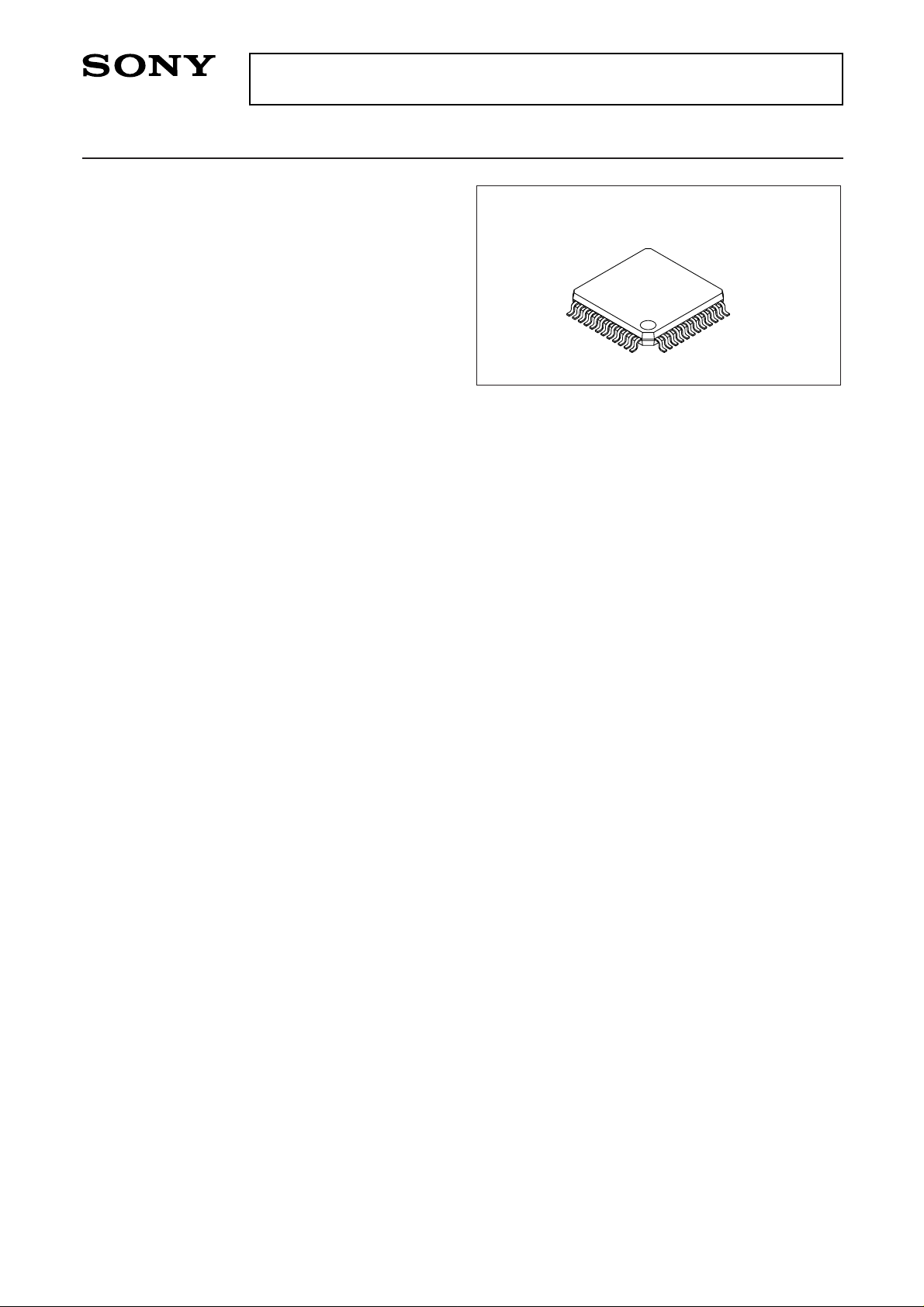
• Package: 48pin TQFP
Structure
Bi-CMOS IC
Applications
Small liquid crystal monitor
Absolute Maximum Ratings (Ta = 25°C)
• Supply voltage VCC
∗1
7.0 V
VVG
∗2
7.0 V
VVC
∗3
≤ VCC + 0.2 V
VVG
∗4
≥ GND – 0.2 V
• Operating temperature
Topr –25 to +85 °C
• Storage temperature
Tstg –55 to +150 °C
• Allowable power dissipation (Ta ≤ 25°C)
Pd 1.72 W
• Reduced ratio (Ta < 25°C) 13.8 mW/°C
Operating Conditions
• Supply voltage VCC
∗1
4.5 to 5.0 to 5.5 V
VVG
∗2
4.0 to VCC V
VVC
∗3
4.0 to VCC V
VVG
∗4
0 to 1.0 V
∗1
Applied to Vcc – GND.
∗2
Applied to COMVcc – COMGND
∗3
Applied to COMVcc – GND
∗4
Applied to COMGND – GND
– 1 –
E99617-PS
Sony reserves the right to change products and specifications without prior notice. This information does not convey any license by
any implication or otherwise under any patents or other right. Application circuits shown, if any, are typical examples illustrating the
operation of the devices. Sony cannot assume responsibility for any problems arising out of the use of these circuits.
CXD2475TQ
48 pin TQFP (Plastic)
– 2 –
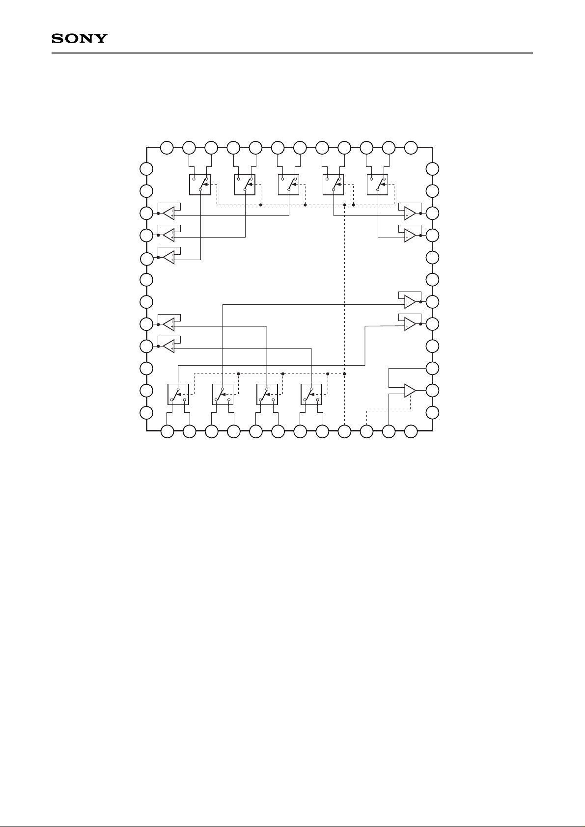
CXD2475TQ
Block Diagram
1 2 3 4 5 6 7 8 9 10 11 12
13
14
15
16
17
18
19
20
21
22
23
24
252627282930313233343536
37
38
39
40
41
42
43
44
45
46
47
48
NC
GND
V7
V8
NC
Vcc
V2
V3
GND
COMVcc
COMOUT
NC
buff
NC
GND
V6
V5
V4
NC
Vcc
V1
V0
GND
NC
NC
VH3
VL3
VH2
VL2
VH1
VL1
VH0
VL0
SW
COMSW
COMGND
NC
NC
VL4
VH4
VL5
VH5
VL6
VH6
VL7
VH7
VL8
VH8
NC
– 3 –
CXD2475TQ
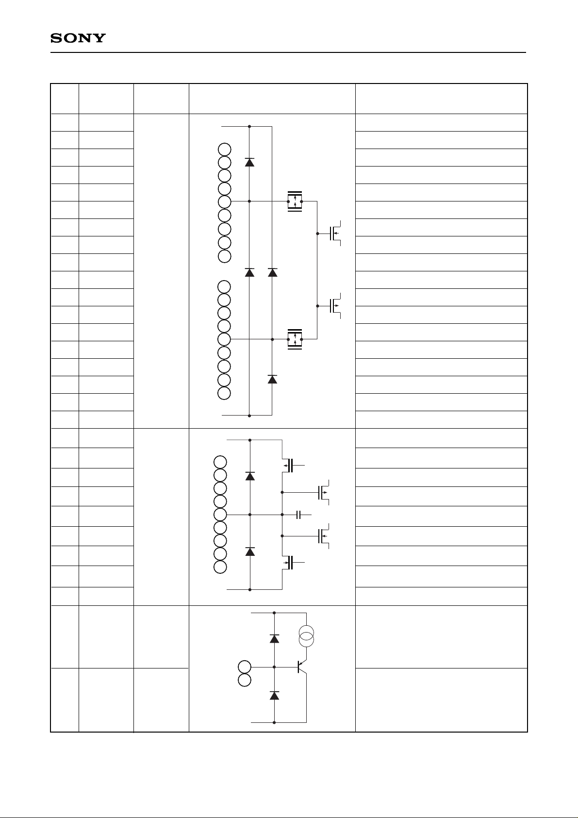
Pin Description
Pin
No.
Symbol Pin voltage Equivalent circuit Description
1 VH3
0.2 to 4.8V
DC input when SW is high.
2
VL3
DC input when SW is low.
3 VH2
DC input when SW is high.
4 VL2
DC input when SW is low.
5 VH1
DC input when SW is high.
6 VL1
DC input when SW is low.
7 VH0
DC input when SW is high.
8 VL0
DC input when SW is low.
26 VH8
DC input when SW is high.
27 VL8
DC input when SW is low.
28 VH7
DC input when SW is high.
29 VL7
DC input when SW is low.
30 VH6
DC input when SW is high.
31 VL6
DC input when SW is low.
32 VH5
DC input when SW is high.
33 VL5
DC input when SW is low.
34 VH4
DC input when SW is high.
35 VL4
DC input when SW is low.
0.2 to 4.8V
17 V3
V3 output.
18 V2
V2 output.
21 V8
V8 output.
22 V7
V7 output.
39 V6
V6 output.
40 V5
V5 output.
41
V4
V4 output.
44 V1
V1 output.
45
V0
V0 output.
9 SW
Input switch.
VL is output for low; VH for high.
10 COMSW
COM output switch.
COMVcc level is output for low;
COMGND level for high.
2
4
6
29
31
33
35
Vcc
GND
VH
VL
8
27
1
3
5
7
26
28
30
32
34
Vcc
GND
39
22
40
18
17
21
44
41
45
Vcc
GND
9
10
 Loading...