

Sony CXD2470R Datasheet
Timing Generator for Frame Readout CCD Image Sensor
Description
The CXD2470R is a timing generator IC which
generates the timing pulses for performing frame
readout using the ICX224,ICX284,ICX202 and ICX232
CCD image sensor.
Features
• Base oscillation frequency 24.00 to 36.00MHz (max.)
• High-speed/low-speed shutter function
• Supports quadruple-speed readout drive
• Horizontal driver for CCD image sensor
• Vertical driver for CCD image sensor
Applications
Digital still cameras
Structure
Silicon gate CMOS IC
Applicable CCD Image Sensors
ICX224 (Type 1/2, 2020K pixels)
ICX284 (Type 1/2.7, 2020K pixels)
ICX202 (Type 1/3, 1250K pixels)
ICX232 (Type 1/3.6, 1250K pixels)
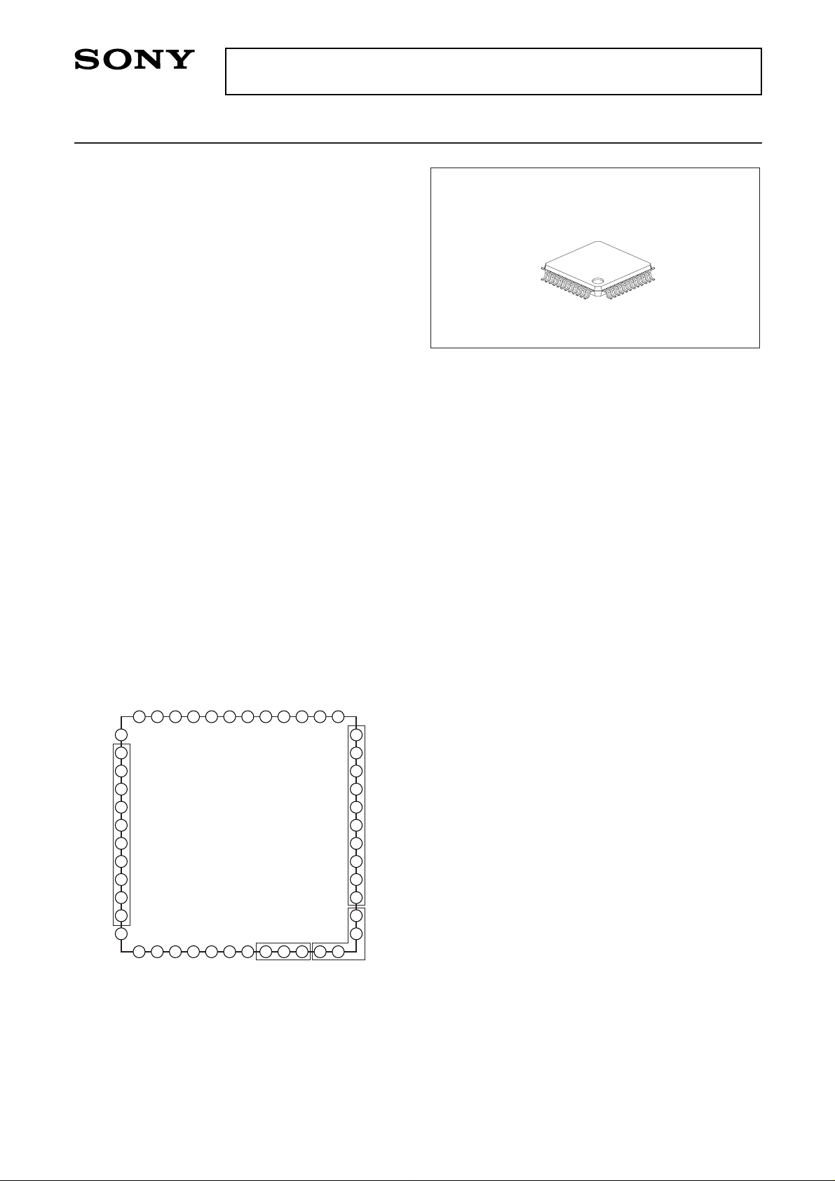
Pin Configuration
Absolute Maximum Ratings
• Supply voltage VDD VSS – 0.3 to +7.0 V
VL –10.0 to VSS V
VH VL – 0.3 to +26.0 V
• Input voltage VI VSS – 0.3 to VDD + 0.3 V
• Output voltage VO1 VSS – 0.3 to VDD + 0.3 V
VO2 VL – 0.3 to VSS + 0.3 V
VO3 VL – 0.3 to VH + 0.3 V
• Operating temperature
Topr –20 to +75 °C
• Storage temperature
Tstg –55 to +150 °C
Recommended Operating Conditions
• Supply voltage VDDb 3.0 to 5.5 V
VDDa, VDDc, VDDd
3.0 to 3.6 V
VM 0.0 V
VH 14.5 to 15.5 V
VL –7.0 to –8.0 V
• Operating temperature
Topr –20 to +75 °C
– 1 –
E98Y31C9Z-PS
Sony reserves the right to change products and specifications without prior notice. This information does not convey any license by
any implication or otherwise under any patents or other right. Application circuits shown, if any, are typical examples illustrating the
operation of the devices. Sony cannot assume responsibility for any problems arising out of the use of these circuits.
CXD2470R
48 pin LQFP (Plastic)
∗
Groups of pins enclosed in the figure indicate
sections for which power supply separation is
possible.
1 2 3 4 5 6 7 8 9 10 11 12
13
14
15
16
17
18
19
20
21
22
23
24
2526272829
30
313233343536
37
38
39
40
41
42
43
44
45
46
47
48
H2
V
DD3
V
DD4
XSHP
XSHD
XRS
PBLK
CLPDM
V
SS4
OBCLP
ADCLK
V
SS5
CKO
CKI
OSCO
OSCI
V
DD5
MCKO
SSI
SCK
SEN
VDI
HDI
V
SS6
H1
V
SS3VSS2
RG
V
DD2
EBCKSM
V
DD1
WEN
ID
DSGAT
RST
V
SS1
TEST2
SUB
V3B
VL
V3A
V1B
VH
V1A
V4
V2
VM
TEST1
– 2 –
CXD2470R
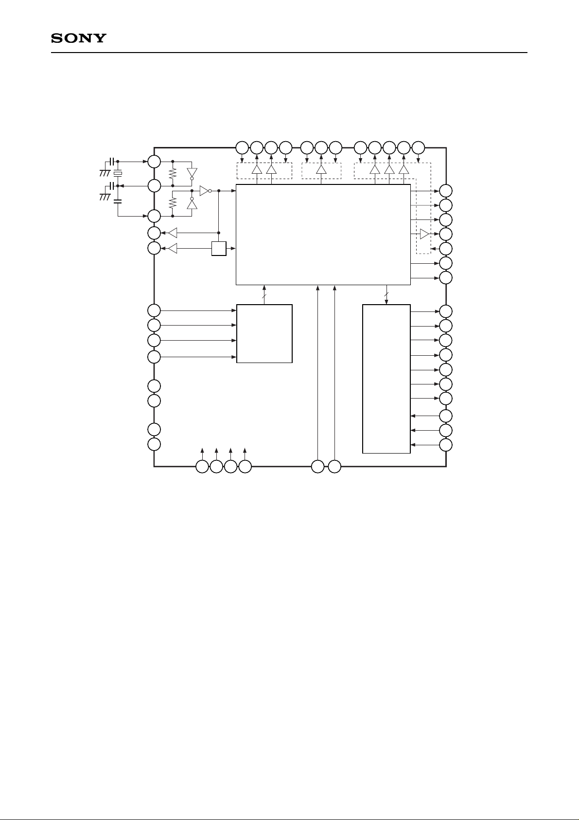
Block Diagram
3 2 37 48 35 34
39
44
43
41
5
4
24
23
22
20
19
2118171615
10
9811131214
28
27
26
25
30
7
29
1
V1B
V2
V3A
V1A
WEN
ID
V
SS5
ADCLK
OBCLP
CLPDM
PBLK
VSS4
XRS
XSHD
XSHP
V
DD4
V
SS2
RG
V
DD2
V
SS3
H2
H1
V
DD3
VDI
HDI
TEST2
TEST1
RST
DSGAT
VSS1
36
V
SS6
V
DD5
V
DD1
MCKO
CKO
CKI
OSCO
OSCI
Pulse Generator
45
38
42
47
40
46
VL
VM
VH
SUB
V4
V3B
31
32
33
SEN
SCK
SSI
Register
V Driver
6
EBCKSM
1/2
– 3 –
CXD2470R
Pin Description
GND
Internal system reset input. High: Normal operation, Low: Reset control
Normally apply reset during power-on.
Schmitt trigger input/No protective diode on power supply side
Control input used to stop pulse generation.
High: Normal operation, Low: Stop control
Schmitt trigger input/No protective diode on power supply side
Vertical direction line identification pulse output.
Memory write timing pulse output.
CHKSUM enable. High: Sum check invalid, Low: Sum check valid
With pull-down resistor
3.3V power supply. (Power supply for common logic block)
3.3V power supply. (Power supply for RG)
CCD reset gate pulse output.
GND
GND
CCD horizontal register clock output.
CCD horizontal register clock output.
3.3 to 5.0V power supply. (Power supply for H1/H2)
3.3V power supply. (Power supply for CDS block)
CCD precharge level sample-and-hold pulse output.
CCD data level sample-and-hold pulse output.
Sample-and-hold pulse output for analog/digital conversion phase alignment.
Pulse output for horizontal and vertical blanking period pulse cleaning.
CCD dummy signal clamp pulse output.
GND
CCD optical black signal clamp pulse output.
Clock output for analog/digital conversion IC.
Logical phase adjustment possible using the serial interface data.
GND
Inverter output.
Inverter input.
Inverter output for oscillation. When not used, leave open or connect a capacitor.
Inverter input for oscillation. When not used, fix low.
3.3V power supply. (Power supply for common logic block)
System clock output for signal processing IC.
1
2
3
4
5
6
7
8
9
10
11
12
13
14
15
16
17
18
19
20
21
22
23
24
25
26
27
28
29
30
VSS1
RST
DSGAT
ID
WEN
EBCKSM
VDD1
VDD2
RG
VSS2
VSS3
H1
H2
VDD3
VDD4
XSHP
XSHD
XRS
PBLK
CLPDM
VSS4
OBCLP
ADCLK
VSS5
CKO
CKI
OSCO
OSCI
VDD5
MCKO
—
I
I
O
O
I
—
—
O
—
—
O
O
—
—
O
O
O
O
O
—
O
O
—
O
I
O
I
—
O
Pin
No.
Symbol
I/O Description
– 4 –
CXD2470R
Serial interface data input for internal mode settings.
Schmitt trigger input/No protective diode on power supply side
Serial interface clock input for internal mode settings.
Schmitt trigger input/No protective diode on power supply side
Serial interface strobe input for internal mode settings.
Schmitt trigger input/No protective diode on power supply side
Vertical sync signal input. Schmitt trigger input
Horizontal sync signal input. Schmitt trigger input
GND
IC test pin 1; normally fixed to GND. With pull-down resistor
GND (GND for vertical driver)
CCD vertical register clock output.
CCD vertical register clock output.
CCD vertical register clock output.
15.0V power supply. (Power supply for vertical driver)
CCD vertical register clock output.
CCD vertical register clock output.
–7.5V power supply. (Power supply for vertical driver)
CCD vertical register clock output.
CCD electronic shutter pulse output.
IC test pin 2; normally fixed to GND. With pull-down resistor
31
32
33
34
35
36
37
38
39
40
41
42
43
44
45
46
47
48
SSI
SCK
SEN
VDI
HDI
VSS6
TEST1
VM
V2
V4
V1A
VH
V1B
V3A
VL
V3B
SUB
TEST2
I
I
I
I
I
—
I
—
O
O
O
—
O
O
—
O
O
I
Pin
No.
Symbol
I/O
Description
– 5 –
CXD2470R
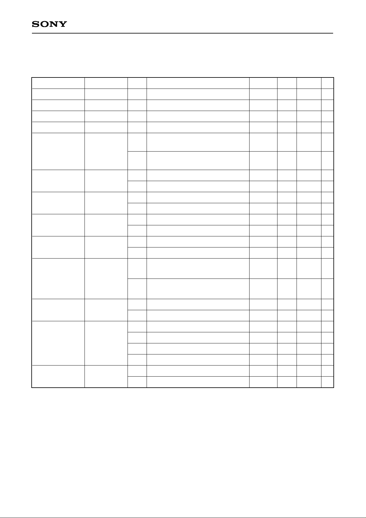
Electrical Characteristics
DC Characteristics (Within the recommended operating conditions)
VDD2
VDD3
VDD4
VDD1, VDD5
RST, DSGAT,
SSI, SCK,
SEN,
EBCKSM
TEST1,
TEST2
VDI, HDI
H1, H2
RG
XSHP, XSHD,
XRS, PBLK,
OBCLP,
CLPDM,
ADCLK
CKO, MCKO
V1A, V1B,
V3A, V3B,
V2, V4
SUB
VDDa
VDDb
VDDc
VDDd
Vt+
Vt–
VIH1
VIL1
VIH2
VIL2
VOH1
VOL1
VOH2
VOL2
VOH3
VOL3
VOH4
VOL4
IOL
IOM1
IOM2
IOH
IOSL
IOSH
3.0
3.0
3.0
3.0
0.8VDDd
0.7VDDd
0.7VDDd
VDDb – 0.8
VDDb – 0.8
VDDc – 0.8
VDDd – 0.8
10.0
5.0
5.4
3.3
3.3
3.3
3.3
3.6
5.5
3.6
3.6
0.2VDDd
0.3VDDd
0.3VDDd
0.4
0.4
0.4
0.4
–5.0
–7.2
–4.0
V
V
V
V
V
V
V
V
V
V
V
V
V
V
V
V
V
V
mA
mA
mA
mA
mA
mA
Feed current where IOH = –22.0mA
Pull-in current where IOL = 14.4mA
Feed current where IOH = –3.3mA
Pull-in current where IOL = 2.4mA
Feed current where IOH = –3.3mA
Pull-in current where IOL = 2.4mA
Feed current where IOH = –10.4mA
Pull-in current where IOL = 7.2mA
V1A/B, V2, V3A/B, V4 = –8.25V
V1A/B, V2, V3A/B, V4 = –0.25V
V1A/B, V3A/B = 0.25V
V1A/B, V3A/B = 14.75V
SUB = –8.25V
SUB = 14.75V
Supply voltage 1
Supply voltage 2
Supply voltage 3
Supply voltage 4
Input voltage 1
∗1
Input voltage 2
∗2
Input voltage 3
Output voltage 1
Output voltage 2
Output voltage 3
Output voltage 4
Output current 1
Output current 2
Item Pins
Symbol
Conditions Min. Typ. Max. Unit
∗1
These input pins are Schmitt trigger inputs and do not have protective diodes on the internal power supply
side.
∗2
These input pins have internal pull-down resistors.
Note) The above table indicates the condition for 3.3V drive.
– 6 –
CXD2470R
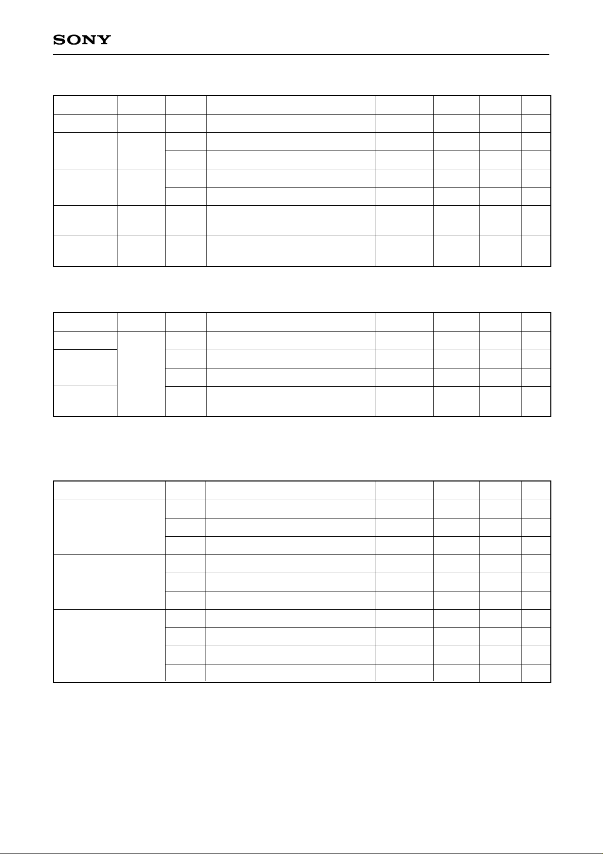
Inverter I/O Characteristics for Oscillation (Within the recommended operating conditions)
Item
Logical Vth
Input
voltage
Output
voltage
Feedback
resistor
Oscillation
frequency
Pins
OSCI
OSCI
OSCO
OSCI,
OSCO
OSCI,
OSCO
Symbol
LVth
VIH
VIL
VOH
VOL
RFB
f
Conditions
Feed current where IOH = –3.6mA
Pull-in current where IOL = 2.4mA
VIN = VDDd or VSS
Min.
0.7VDDd
VDDd – 0.8
500k
20
Typ.
VDDd/2
2M
Max.
0.3VDDd
0.4
5M
50
Unit
V
V
V
V
V
Ω
MHz
Item
Logical Vth
Input
voltage
Input
amplitude
Pins
CKI
Symbol
LVth
VIH
VIL
VIN
Conditions
fmax 50MHz sine wave
Min.
0.7VDDd
0.3
Typ.
VDDd/2
Max.
0.3VDDd
Unit
V
V
V
Vp-p
Item
Rise time
Fall time
Output noise voltage
Symbol
TTLM
TTMH
TTLH
TTML
TTHM
TTHL
VCLH
VCLL
VCMH
VCML
Conditions
VL to VM
VM to VH
VL to VH
VM to VL
VH to VM
VH to VL
Min.
200
200
30
200
200
30
Typ.
350
350
60
350
350
60
Max.
500
500
90
500
500
90
1.0
1.0
1.0
1.0
Unit
ns
ns
ns
ns
ns
ns
V
V
V
V
Inverter Input Characteristics for Base Oscillation Clock Duty Adjustment
(Within the recommended operating conditions)
Note) Input voltage is the input voltage characteristics for direct input from an external source. Input amplitude
is the input amplitude characteristics in the case of input through a capacitor.
Switching Characteristics (VH = 15.0V, VM = GND, VL = –7.5V)
Notes) 1. The MOS structure of this IC has a low tolerance for static electricity, so full care should be given for
measures to prevent electrostatic discharge.
2. For noise and latch-up countermeasures, be sure to connect a by-pass capacitor (0.1µF or more)
between each power supply pin (VH, VL) and GND.
3. To protect the CCD image sensor, clamp the SUB pin output at VH before input to the CCD image
sensor.
– 7 –
CXD2470R
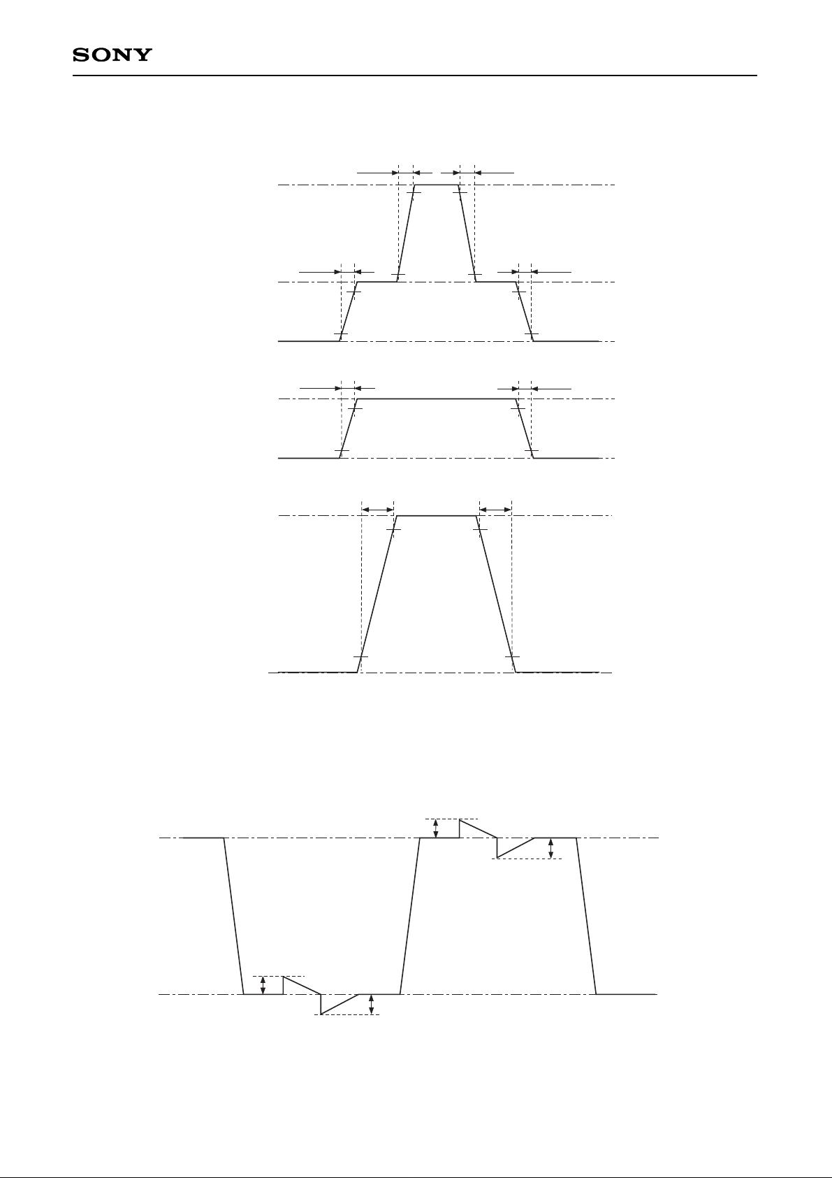
Switching Waveforms
V1A (V1B, V3A, V3B)
V2 (V4)
SUB
TTMH TTHM
VH
VM
VL
VM
VL
VH
VL
90%
10%
90%
10%
TTLM
TTLM
90%
10%
90%
10%
TTLH TTHL
90%90%
10% 10%
TTML
90%
10%
TTML
90%
10%
Waveform Noise
VCMH
VCML
V
H
VL
VCLH
VCLL
– 8 –
CXD2470R
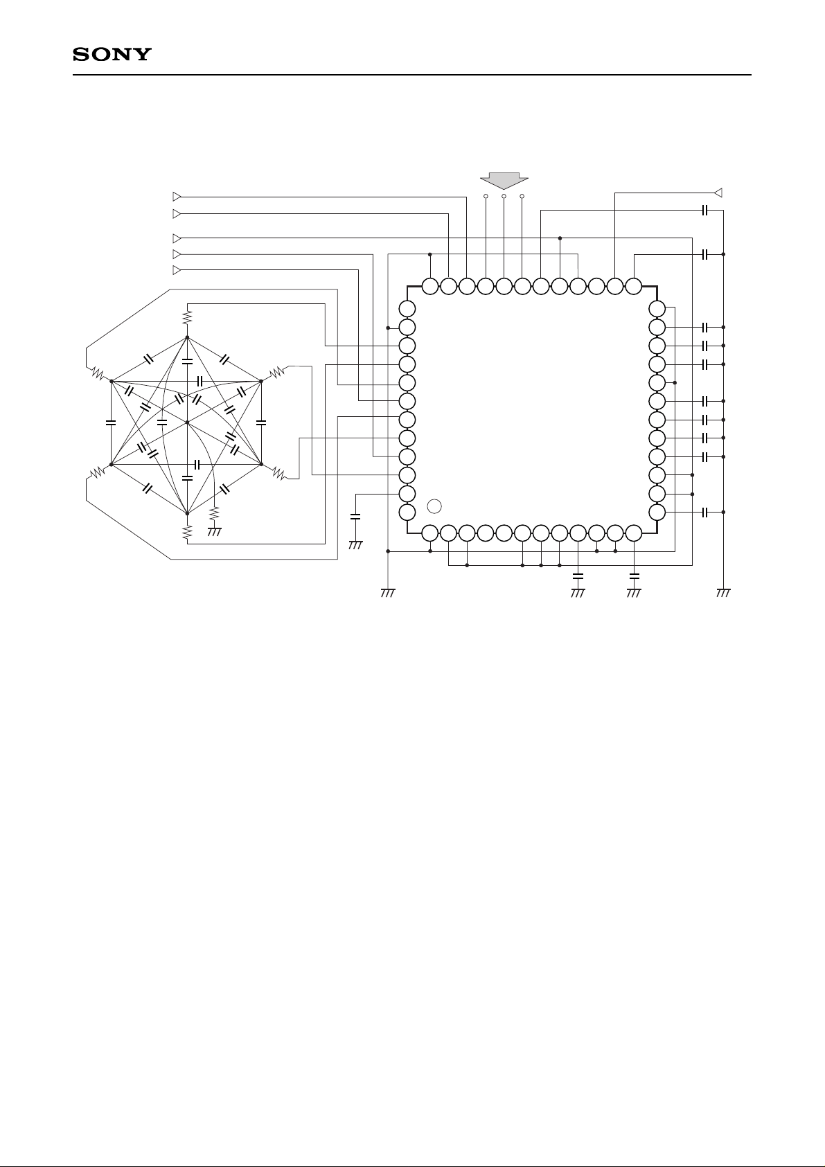
Measurement Circuit
1 2 3 4 5 6 7 8 9 10 11 12
13
14
15
16
17
18
19
20
21
22
23
24
2526272829
30
313233343536
37
38
39
40
41
42
43
44
45
46
47
48
VDI
CKI
C6
C6
C6
C6
C6
C6
C6
C6
C6
C5
C5C4
C3
CXD2470R
Serial interface data
HDI
+3.3V
–7.5V
+15.0V
C2
C2 C2
C2
C2
R1
R1
R1
R2
R1
R1 R1
C2
C2
C2
C2
C2
C2
C2
C2
C2
C1
C1
C1
C1
C1
C1
C2
C1 3300pF C2 560pF C3 820pF C4 30pF C5 180pF C6 10pF
R1 30Ω R2 10Ω
– 9 –
CXD2470R
AC Characteristics
AC characteristics between the serial interface clocks
SSI
0.2V
DDd
0.2VDDd
0.8VDDd
ts2
th1ts1
ts3
0.8V
DDd
0.8VDDd
SCK
SEN
SEN
Symbol
ts1
th1
ts2
ts3
Definition
SSI setup time, activated by the rising edge of SCK
SSI hold time, activated by the rising edge of SCK
SCK setup time, activated by the rising edge of SEN
SEN setup time, activated by the rising edge of SCK
Min. Typ. Max.
20
20
80
20
Unit
ns
ns
ns
ns
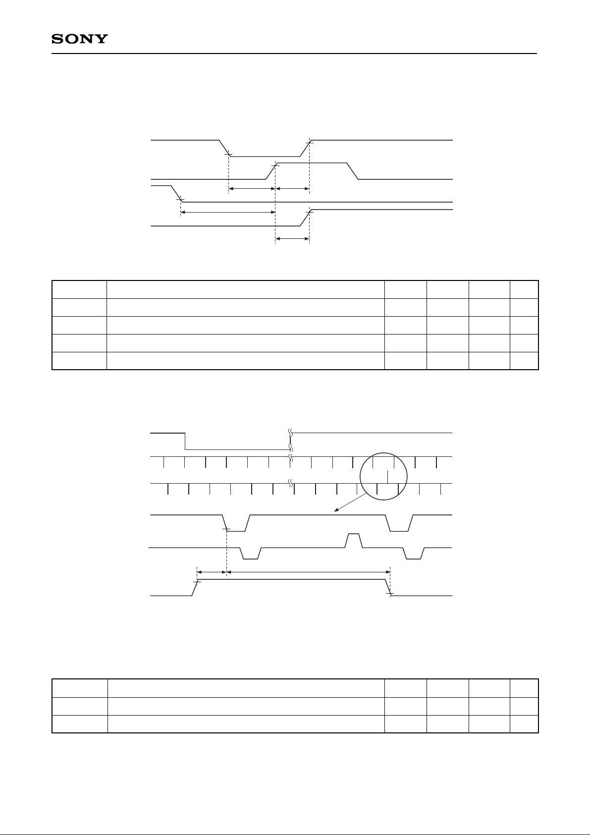
Serial interface clock internal loading characteristics (1)
(Within the recommended operating conditions)
th1
Enlarged view
Example: During frame mode
0.2V
DDd
ts1
0.2V
DDd
V1A
VDI
HDI
HDI
V1A
SEN
0.8V
DDd
Symbol
ts1
th1
Definition
SEN setup time, activated by the falling edge of HDI
SEN hold time, activated by the falling edge of HDI
Min. Typ. Max.
0
102
Unit
ns
µs
∗
Be sure to maintain a constantly high SEN logic level near the falling edge of the HDI in the horizontal period
during which V1A/B and V3A/B values take the ternary value and during that horizontal period.
(Within the recommended operating conditions)
– 10 –
CXD2470R
Serial interface clock output variation characteristics
Normally, the serial interface data is loaded to the CXD2470R at the timing shown in "Serial interface clock
internal loading characteristics (1)" above. However, one exception to this is when the data such as STB is
loaded to the CXD2470R and controlled at the rising edge of SEN. See "Description of Operation".
0.8VDDd
SEN
Output signal
tpdPULSE
Symbol
tpdPULSE
Definition
Output signal delay, activated by the rising edge of SEN
Min. Typ. Max.
1005
Unit
ns
(Within the recommended operating conditions)
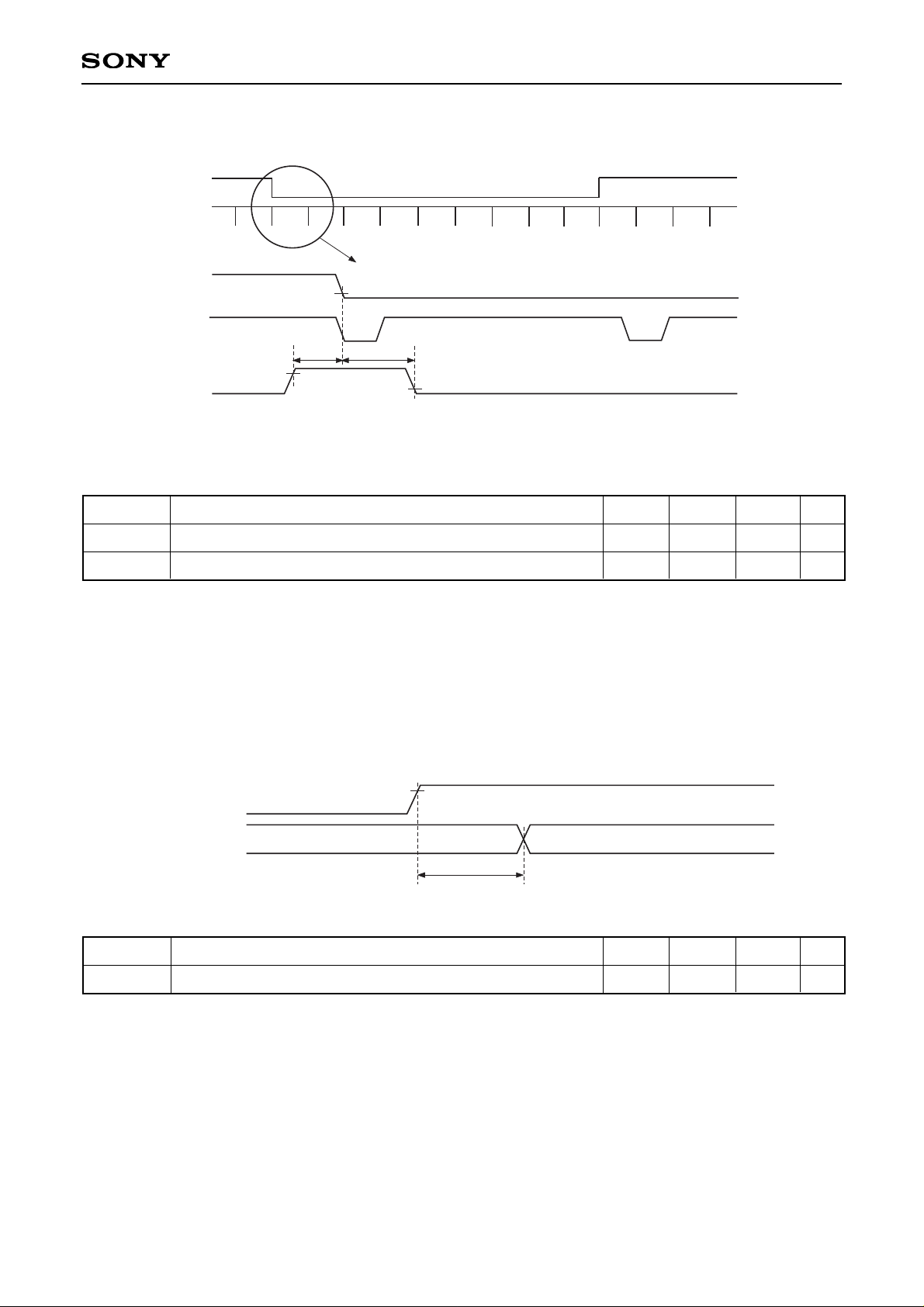
Serial interface clock internal loading characteristics (2)
th1
Enlarged view
0.2V
DDd
ts1
0.2V
DDd
VDI
HDI
VDI
HDI
SEN
0.8V
DDd
Example: During frame mode
Symbol
ts1
th1
Definition
SEN setup time, activated by the falling edge of VDI
SEN hold time, activated by the falling edge of VDI
Min. Typ. Max.
0
200
Unit
ns
ns
∗
Be sure to maintain a constantly high SEN logic level near the falling edge of VDI.
(Within the recommended operating conditions)
– 11 –
CXD2470R
RST
0.2VDDd
tw1
0.8VDDd
VDI, HDI
MCKO
ts1
th1
0.2V
DDd
0.8VDDd
0.2VDDd
RST loading characteristics
Symbol
tw1
Definition
RST pulse width
Min. Typ. Max.35Unit
ns
(Within the recommended operating conditions)
VDI and HDI loading characteristics
Symbol
ts1
th1
Definition
VDI and HDI setup time, activated by the rising edge of MCKO
VDI and HDI hold time, activated by the rising edge of MCKO
Min. Typ. Max.
20
5
Unit
ns
ns
MCKO load capacitance = 10pF
∗1
(Within the recommended operating conditions)
DSGAT
H1, H2, RG, XSHP, XSHD, XRS,
ADCLK, PBLK, CLPDM, OBCLP
tpDSGAT
0.2V
DDd
0.2VDDd
Output timing characteristics using DSGAT
H1 and H2 load capacitance = 180pF, RG load capacitance = 30pF,
XSHP, XSHD, XRS, PBLK, CLPDM, OBCLP and ADCLK load capacitance = 10pF
(Within the recommended operating conditions)
Symbol
tpDSGAT
Definition
Time until the above outputs go low after the fall of DSGAT
Min. Typ. Max.
100
Unit
ns
– 12 –
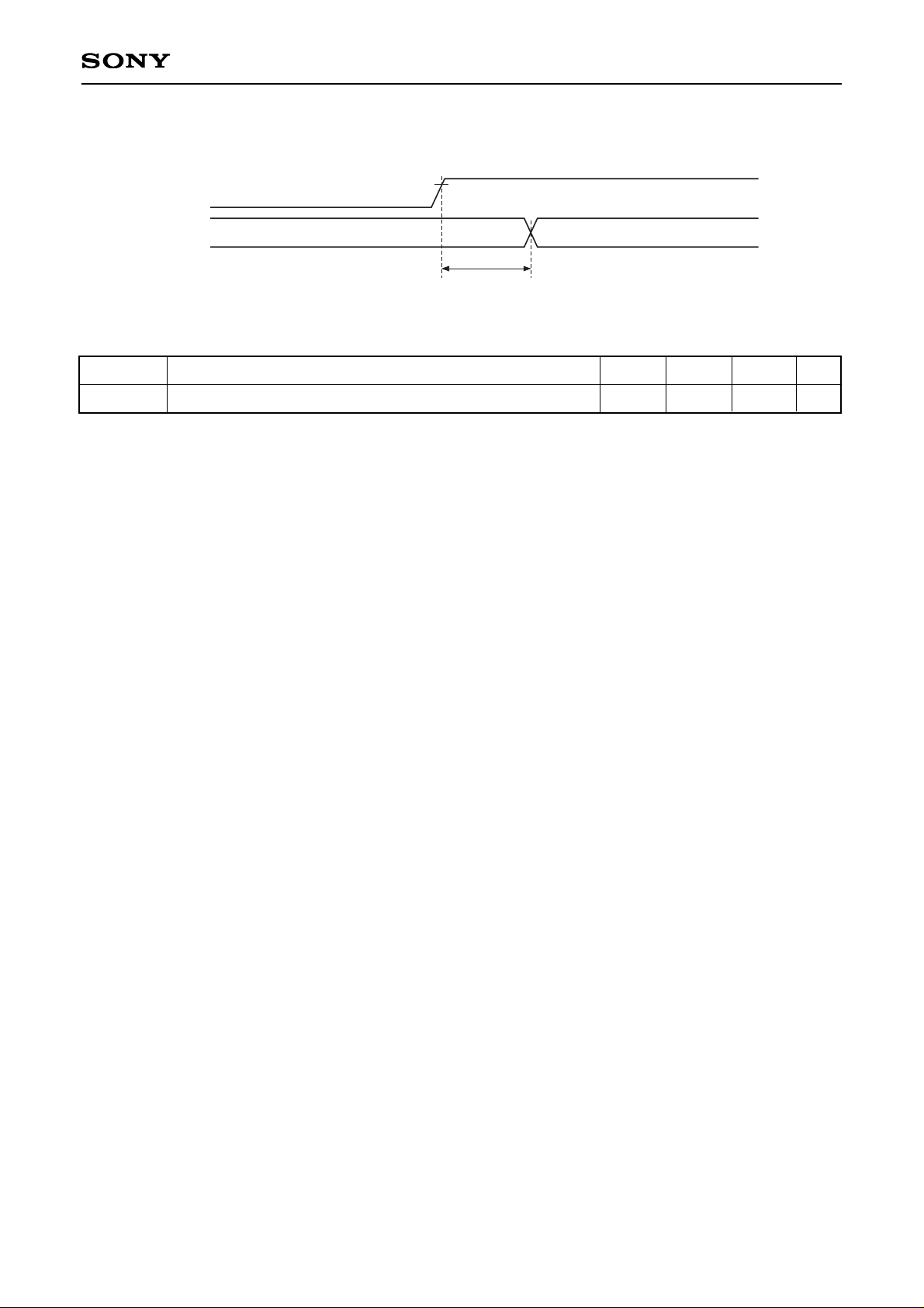
CXD2470R
0.8VDDd
MCKO
WEN, ID
tpd1
WEN and ID load capacitance = 10pF
(Within the recommended operating conditions)
Symbol
tpd1
Definition
Time until the above outputs change after the rise of MCKO
Min. Typ. Max.
6020
Unit
ns
Output variation characteristics
 Loading...